Part number width specifications are the width-related dimensions tied to an exact manufacturer part number, usually found in its datasheet package drawing. They may include package body width, overall lead span, terminal width, exposed-pad width, recommended land-pattern width, and packing width. The part number itself may identify a package option, but it rarely gives enough dimensional information to create or approve a PCB footprint without the matching manufacturer drawing.
The safest workflow is to verify the full manufacturer part number (MPN), open the current manufacturer datasheet, match the ordering suffix to the package code, and then read the minimum, nominal, and maximum dimensions in the package outline. This prevents a common BOM mistake: selecting a part with the correct electrical function but the wrong physical package.
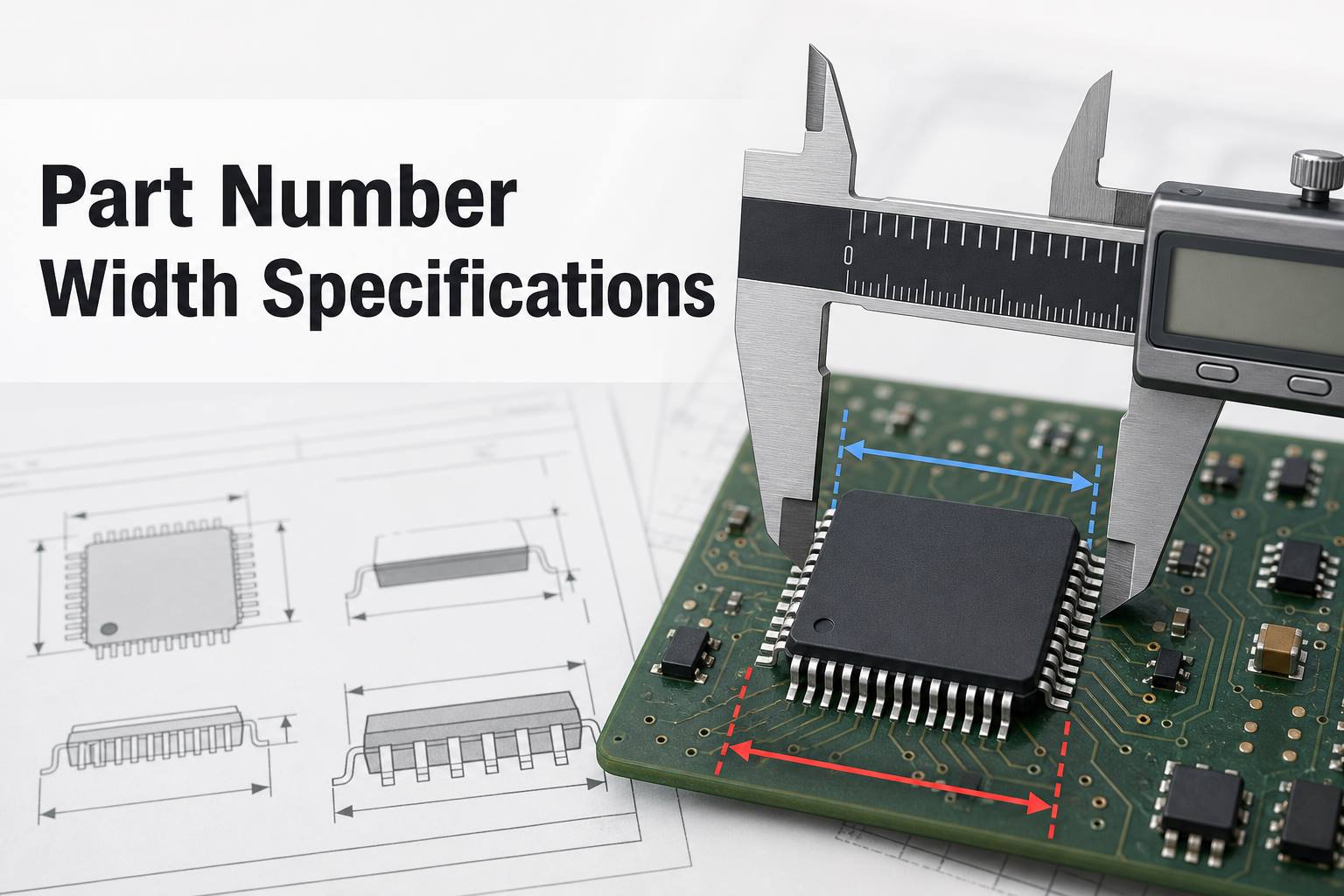
What Does Part Number Width Specification Mean?
A part number width specification is not one universal measurement; it is a set of mechanical dimensions associated with a specific orderable component. Depending on the package, 鈥渨idth鈥?can refer to the molded body, the span across leads, the distance across terminals, an exposed thermal pad, or the tape-and-reel carrier.
This distinction matters because different teams use width differently. A mechanical engineer may need the maximum body envelope. A PCB designer needs terminal geometry and the recommended land pattern. A sourcing engineer must confirm that a proposed alternate uses a compatible package. A production engineer may also need carrier-tape width and component height for feeder setup.
| Width term | What it measures | Why it matters |
| Body width | Molded or ceramic package body, normally excluding leads | Courtyard, enclosure clearance, neighboring-component spacing |
| Overall width or lead span | Distance across the outermost leads or terminals | Footprint fit, solder-joint geometry, inspection access |
| Terminal width | Width of one lead, contact or termination | Pad width, solder fillet and inspection criteria |
| Exposed-pad width | Width of a thermal or ground pad under the package | Stencil aperture, heat transfer, voiding and grounding |
| Land-pattern width | Overall span of the recommended PCB pads | Assembly yield and solder-joint reliability |
| Carrier-tape width | Width of the tape used for automated placement | Feeder selection and incoming material planning |
Can You Read Width Directly from a Part Number?
Sometimes a part number contains a package or size code, but the code must be decoded with that manufacturer ordering guide. There is no universal rule that makes every suffix equal to a specific width.
For chip resistors and capacitors, codes such as 0402, 0603 and 0805 often describe a nominal length-by-width format. However, the same four digits can be interpreted in imperial or metric notation. An imperial 0603 is approximately 1.6 * 0.8 mm, while a metric 0603 is approximately 0.6 * 0.3 mm. The manufacturer, product family and datasheet determine which system applies.
For ICs, suffixes may indicate package family, pin count, temperature grade, packing method, lead finish or qualification option. Two electrically similar parts can have different widths because one uses SOIC, TSSOP, QFN or another package. Never remove the suffix during BOM cleanup unless the approved manufacturer documentation proves it is nonessential.
Where Are Width Dimensions Found in a Datasheet?
Width dimensions are normally located in the mechanical package drawing, package outline, dimensions section, or a separate package-document link referenced by the datasheet. The ordering-information table connects the exact MPN to the correct package name or drawing code.
- Search the exact MPN on the component manufacturer official website.
- Confirm the device family, revision and orderable status.
- Find the ordering guide and match the full suffix to the package option.
- Open the corresponding package outline drawing.
- Check the drawing units, dimension symbols, notes and tolerances.
- Use the recommended land pattern when one is provided; do not copy the body outline as the copper-pad outline.
Dimension letters vary by drawing system and package family. For example, a drawing may use one symbol for body width and another for overall width. Read the legend on that exact drawing instead of assuming that a familiar letter always means the same feature.
Body Width vs Overall Width vs PCB Land Pattern
Body width describes the component housing, overall width includes leads or terminals, and the PCB land pattern describes the copper pads needed to solder the component. These values are related but are not interchangeable.
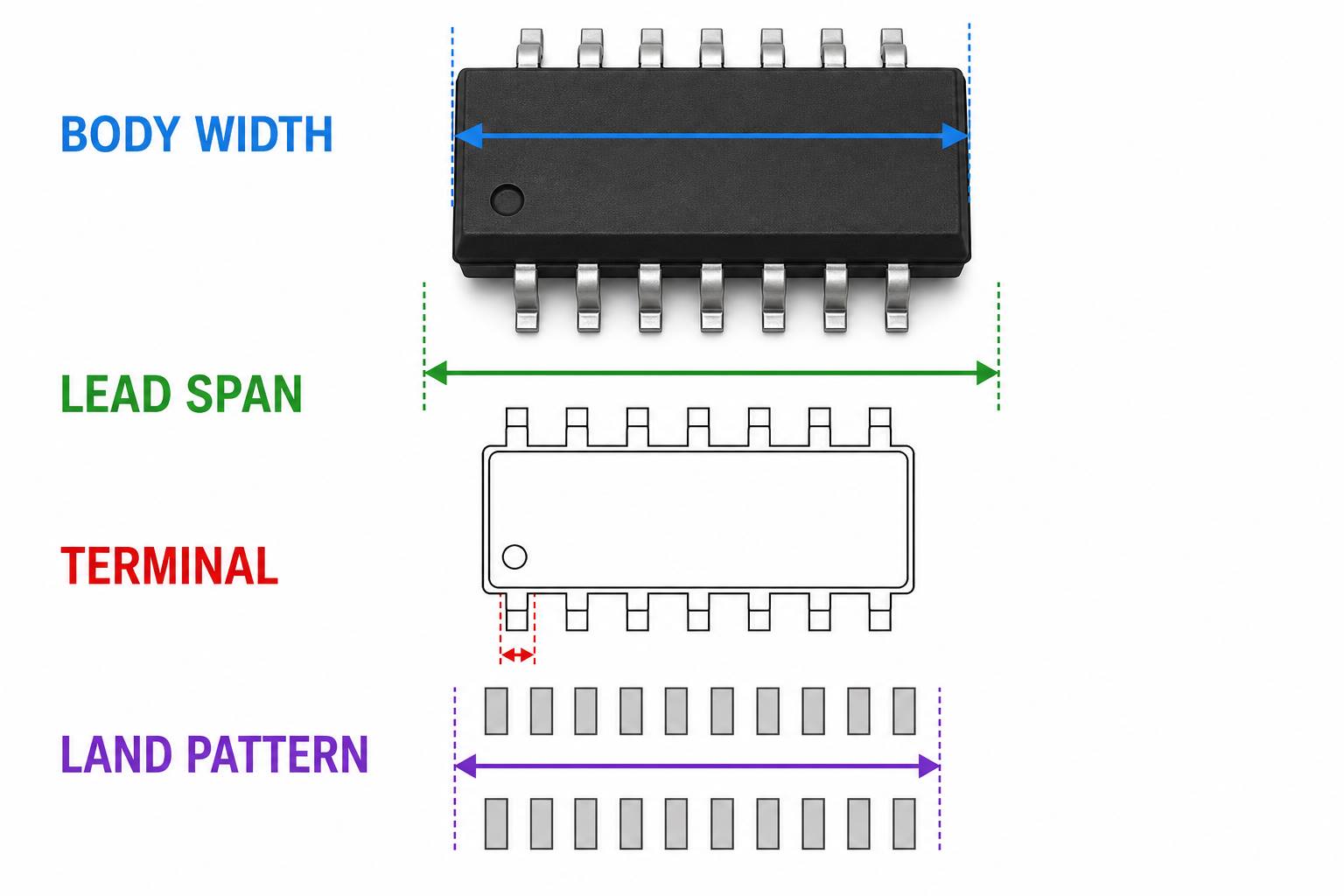
A common footprint error occurs when a designer treats the maximum package body width as the pad span. Gull-wing leads extend beyond the body and require toe, heel and side solder allowances. Leadless packages such as QFN use a different geometry, often including a central exposed pad and tightly controlled perimeter terminals. Connectors may add locating pegs, shell tabs, board-edge offsets or mating-envelope requirements beyond the visible contact width.
Use the manufacturer recommended footprint as the starting point, then review it against the PCB assembly process, solder paste, inspection method, density, rework access and the applicable company or industry land-pattern policy.
How to Interpret Minimum, Nominal and Maximum Width
Minimum and maximum values define the allowed manufacturing envelope; the nominal value is a reference target and may not represent every delivered part. PCB clearance and mechanical fit should normally account for the maximum component envelope, while solder-joint design must consider the complete terminal tolerance range.
Datasheets express tolerances in several ways: explicit minimum and maximum columns, a nominal value with plus/minus tolerance, or a basic dimension controlled by drawing notes. Units may be millimeters, inches, or both. Do not convert a rounded catalog value into a manufacturing limit. Use the dimension table attached to the package drawing and keep enough decimal precision to avoid changing the tolerance.
- Use maximum body and lead span for keep-out and enclosure checks.
- Use terminal minimum and maximum dimensions for pad and solder-joint review.
- Use maximum height for enclosure, shielding and pick-and-place clearance.
- Use the recommended footprint dimensions for PCB pads, not a visual estimate.
- Check whether dimensions exclude mold flash, plating, burrs or terminal deformation.
How Common Package Codes Relate to Width
Package codes are useful search clues, but only the exact package drawing establishes the controlling width. Similar package names can cover different body widths, pitches, terminal styles and pin counts.
| Package or code | Width clue | Required confirmation |
| 0402, 0603, 0805 passives | Often nominal length * width code | Imperial vs metric system, tolerance, height and termination geometry |
| SOIC or SOP | Narrow and wide body variants exist | Body width, lead span, pitch, pin count and package drawing code |
| TSSOP, SSOP, MSOP | Name suggests a small-outline family | Exact pitch, body width, overall span and terminal dimensions |
| QFN or DFN | Often described by nominal body length * width | Terminal layout, exposed pad, wettable flanks and recommended land pattern |
| BGA, LGA or CSP | Body size and array size may both be stated | Ball or land pitch, matrix, missing positions, package height and courtyard |
| SOT family | Family code identifies an outline series | Manufacturer drawing, terminal count, lead form and alternate outline variants |
| Connector series | Part number may encode positions or pitch | Housing width, mating envelope, pegs, shell tabs and board-edge location |
How to Verify an Exact MPN Before PCB Layout or Assembly
The most reliable verification method is a three-way match between the BOM, the official manufacturer package drawing and the PCB library footprint. Distributor filters and third-party CAD models are useful references, but they should not replace the manufacturer source.
- Lock the identity: record the manufacturer name and full MPN, including suffixes.
- Confirm the orderable package: match the MPN to the package code in the ordering guide.
- Record controlling dimensions: body width, lead span, pitch, terminal width, height and exposed-pad dimensions.
- Compare the footprint: verify pad geometry, pin numbering, courtyard, assembly outline and polarity mark.
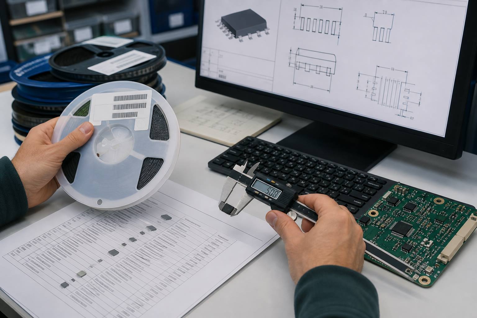
- Check the physical supply: compare reel or tray label, top marking and incoming sample against the approved BOM.
- Approve deviations: treat any package or width difference as an engineering change, not a purchasing convenience.
What Should a BOM Include Besides the Part Number?
A production BOM should include enough information to distinguish the approved component and package without relying on a shortened description. At minimum, use the manufacturer, full MPN, value or function, package or footprint, quantity and reference designators.
Useful additional fields include tolerance, voltage or current rating, dielectric or material, temperature grade, lifecycle status, approved alternates, do-not-fit status and sourcing notes. BestPCBs provides a broader guide on how to make a PCB BOM, while the PCB component identification guide explains how markings, package shape and documentation work together.
| BOM field | Purpose |
| Manufacturer and full MPN | Identifies the exact orderable device |
| Package or approved footprint | Connects the component to PCB land geometry |
| Value, function and ratings | Confirms electrical suitability |
| Reference designators and quantity | Controls placement locations and purchasing quantity |
| Approved alternates | Defines substitutions already reviewed by engineering |
| Revision and source document | Maintains traceability when drawings change |
What Problems Come from Using the Wrong Width?
An incorrect width can cause more than a cosmetic mismatch: it can make placement impossible, reduce solder-joint quality, create shorts, block inspection or interfere with nearby parts and the product enclosure.
- Wrong pad span: leads do not sit correctly on the copper pads.
- Insufficient solder fillet: pads are too short or narrow for the terminal tolerance.
- Bridging risk: pads or stencil apertures do not match the actual pitch and lead width.
- Courtyard collision: the maximum component body overlaps another device, shield or connector.
- Assembly delay: incoming material fails the first-article check and must be replaced or the footprint redesigned.
- Uncontrolled substitution: an alternate fits electrically but uses a different package outline.
If a mismatch is found before production, stop purchasing or placement, identify the controlling drawing revision, compare all affected dimensions, and obtain engineering approval. For unknown parts already on a board, start with the methods in the PCB components identification article rather than relying on one short top mark.
How to Evaluate Alternate Parts with Different Width Specifications
An alternate part is acceptable only when electrical, mechanical, thermal, regulatory and lifecycle requirements have been reviewed together.
Compare the full package drawing, not just the nominal body size. Check pin count and assignment, pitch, terminal style, coplanarity, exposed pad, package height, polarity orientation and the recommended land pattern. Then review the assembly process: paste aperture, reflow profile, AOI or X-ray access, feeder packaging and rework method. The alternate should be added to the approved BOM only after the responsible engineer accepts the comparison.
For projects that need purchasing and package verification support, BestPCBs explains its workflow on the component sourcing page and lists the usual production documents in its PCB assembly FAQ.
Part Number and Package Width Verification Checklist
Use this checklist before footprint release, BOM approval, alternate-part approval and first article assembly.
- Manufacturer name and complete MPN are recorded.
- Ordering suffix matches the intended package and packing method.
- Datasheet and package drawing come from the official manufacturer source.
- Drawing revision and units are confirmed.
- Body width and overall terminal span are not confused.
- Minimum, nominal and maximum dimensions are interpreted correctly.
- Pin pitch, terminal width, package height and exposed pad are checked.
- PCB pads follow an approved land pattern, not the body outline.
- Courtyard, enclosure and rework clearances use the maximum envelope.
- Alternate parts receive documented engineering approval.
- Incoming reel, tray or tube label matches the approved BOM.
- First article inspection confirms orientation and solder-joint geometry.
Frequently Asked Questions
Does the last number in a part number always indicate width?
No. Part-number structures are manufacturer-specific. A final digit or suffix may represent package, tolerance, temperature grade, packing, lead finish or another option. Decode it with the official ordering guide for that product family.
Is component width the same as footprint width?
No. Component width may describe the body or lead span, while footprint width describes the PCB land geometry. Pads usually extend or shift beyond terminal edges to create suitable solder fillets.
Which value should I use when a drawing lists minimum and maximum width?
Use the maximum package envelope for mechanical clearance. For footprint design, evaluate the complete range of terminal and package tolerances or use the manufacturer recommended land pattern.
Why do two distributors show different dimensions for the same MPN?
One listing may use nominal body size while another uses maximum size, overall lead span or rounded catalog data. Resolve the conflict with the current manufacturer datasheet and package drawing.
Are 0603 imperial and 0603 metric components the same size?
No. Imperial 0603 is about 1.6 * 0.8 mm, while metric 0603 is about 0.6 * 0.3 mm. Confirm the notation used by the manufacturer and CAD library.
Can I measure a component with calipers instead of reading the datasheet?
A physical measurement can support incoming inspection, but it cannot replace the drawing. One sample does not define the allowed tolerance, terminal geometry, coplanarity or recommended PCB land pattern.
Does the package name guarantee the same width across manufacturers?
No. Package family names may include multiple outlines, body widths and terminal configurations. Match the exact manufacturer package code and drawing before approving a cross.
What width matters for pick-and-place programming?
Placement setup can require component body dimensions, height, centroid and rotation, while feeder setup also depends on tape width and pocket geometry. Confirm the machine library against the supplied packaging.
Should the BOM contain package dimensions?
The BOM should at least contain the exact MPN and approved package or footprint. Critical dimensions may also be controlled in the library, assembly drawing or approved-parts record for traceability.
What should I send for a PCBA package-fit review?
Send Gerber or native PCB data, the complete BOM, pick-and-place file, assembly drawing, manufacturer datasheets for unusual parts, approved alternates, quantity and test requirements.
Final Takeaway
Part number width specifications must be read as part of a controlled identification chain: exact MPN, ordering code, package drawing, tolerance, PCB land pattern and incoming component. Do not assume that a package name, shortened part number or distributor filter proves mechanical compatibility.
If you are sourcing reliable PCB/PCBA manufacturing, including OEM, ODM, prototyping, mass production or custom engineering solutions, send your BOM, PCB files and package questions to the BestPCBs engineering team for technical support and a quote at sales@bestpcbs.com.