Electrostatic discharge can damage an electronic component in far less time than a person can react. The event may produce a visible spark, but it can also occur without any sound, light, or immediate failure. A device may stop working at once, drift outside its electrical limits, or pass an initial test and fail prematurely in service. Effective prevention therefore cannot depend on whether an operator notices a shock.
The practical answer to how to prevent ESD electrostatic discharge in electronics is to control charge throughout the complete handling route. Keep personnel, tools, work surfaces, and equipment at a common electrical potential; remove avoidable charge generators; neutralize essential insulators; and enclose exposed electronics before they leave an ESD-protected area. A wrist strap, mat, or shielding bag works only as part of this connected system.
What Is ESD and Why Is It Dangerous to Electronics?
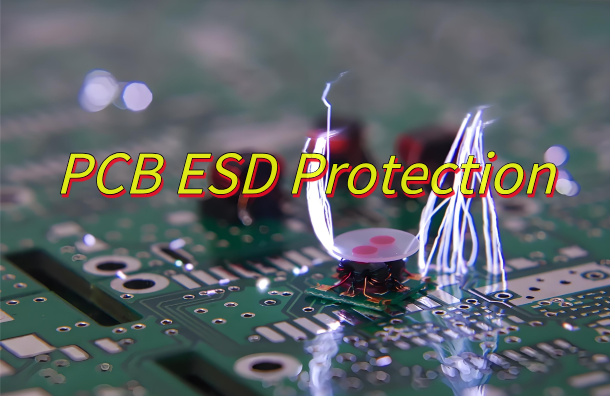
ESD stands for electrostatic discharge: a rapid transfer of charge between objects at different electrical potentials. Static charge can accumulate on a person, cart, plastic tray, garment, tool, or device. When a charged object approaches or makes contact, the potential difference may drive a brief current pulse. That pulse can pass through a semiconductor junction, connector pin, PCB trace, or test point.
The voltage that a person can feel is not a useful pass-or-fail threshold for electronics. Sensitive devices can be affected by discharges below the level of human perception. The resulting damage can be catastrophic, meaning the part fails immediately, or latent, meaning the device is weakened but still appears functional. Latent damage is particularly difficult because ordinary inspection may not reveal it and a basic functional test may not exercise the degraded structure under worst-case conditions.
Prevention must cover both the bare component and every assembly stage in which its conductive contacts remain exposed. A component may be protected in its supplier packaging, then become vulnerable when unpacked, placed on a feeder, manually soldered, moved to inspection, connected to a tester, or transferred into final packaging. The control boundary must follow the item through those transitions.
What Causes Electrostatic Discharge in Electronic Environments?
ESD risk begins when a process generates or moves charge close to exposed electronics. The operator should trace the complete route—from package opening to assembly, testing, storage, and shipment—because a safe bench cannot protect a board during an uncontrolled handoff.
- Contact and separation: Walking, peeling protective film, pulling tape, sliding bins, and removing boards from ordinary foam can cause triboelectric charging. Reduce unnecessary friction and use qualified work surfaces, containers, and packaging.
- People and clothing: Shoes, chairs, synthetic garments, and loose sleeves can generate and retain charge. Use the personnel-grounding method and garments defined for the work area, and keep clothing away from exposed contacts.
- Insulators and induction: A charged plastic object can redistribute charge in a nearby conductor without touching it. Remove unnecessary insulators; where one is essential, assess its field at the product position and use verified ionization when needed.
- Movement and handoffs: Carts, cables, tools, trays, and packaging may introduce a new charge source between workstations. Map every transfer point and close protective packaging before a board leaves the protected environment.
Dry air can allow charge to remain longer, but humidity alone does not make the route safe. Before handling begins, identify the charge generators, conductive paths, exposed pins or pads, and the next location the product will enter.
How Can You Prevent ESD Before Handling Electronic Components?
Preparation is the first control. Many preventable ESD events occur during unpacking or the first transfer because the item is exposed before the area, operator, and destination container are ready. Keep the package closed while you identify the item, prepare the controlled work area, and confirm where the item will be placed if work stops unexpectedly.
Use a deliberate handling sequence:
- Identify ESD sensitivity: check the label, component specification, assembly drawing, or process instruction for the required handling level and packaging. If sensitivity is unknown, do not treat the item as ordinary hardware; keep it protected until the responsible technical owner confirms the controls.
- Choose the handling area before unpacking: move the sealed package to an approved workstation or ESD protected area. Prepare an approved tray or work surface large enough for the item so it will not be placed temporarily on a chair, carton, ordinary bench, or the outside of its packaging.
- Verify personnel and workstation grounding: test the wrist strap or footwear system required for the operation, check the work-surface connection, and respond to any continuous-monitor alarm. A connected cord is not proof of performance; use the specified tester and acceptance criteria.
- Remove or control charge generators: clear ordinary plastic, foam, tape, document sleeves, loose synthetic fabric, and personal items from the immediate area. If an insulating tool, cover, or fixture is essential, position and control it according to the process plan, using verified ionization when required.
- Open the package only after every destination is ready: do not slide the board across the bag, tray, or work surface. Never place an exposed assembly on the outside of a shielding bag. Preserve reusable packaging so the item can be protected immediately if the task is interrupted.
- Handle the item through safe mechanical points: hold boards by their edges and avoid connector contacts, component leads, pads, test points, and exposed conductive areas. Use approved tools or board supports when the item cannot be held securely, and avoid unnecessary hand-to-hand transfers.
- Repackage before any uncontrolled transfer: return the item to a suitable closed package before moving it to storage, another department, or a non-EPA location. Keep the ESD identification visible and ensure the next person knows where the package may be opened.
Electrical safety remains separate from ESD control. Disconnect power and stored-energy sources when the service procedure requires it, but remember that de-energizing equipment does not automatically establish an approved ESD grounding path. Never improvise a connection to an unknown conductor. Use approved grounding hardware and follow the equipment safety procedure; an ESD control measure must not create a shock or equipment hazard.
How Do You Ground Yourself and an ESD Workstation Correctly?
Grounding gives conductive objects and personnel a controlled path toward a common electrical potential. The goal is to connect the operator, work surface, approved conductive fixtures, and designated grounding point through a system that can be tested before sensitive electronics are exposed. Apply this approach according to how the work is performed:
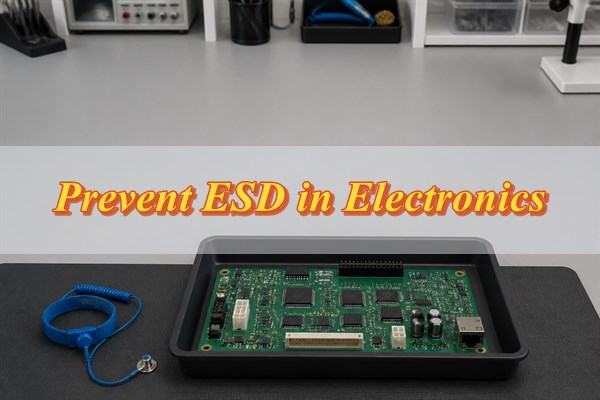
- For seated work, use continuous wrist-strap grounding. Fit the band against bare skin, connect the cord to the designated grounding point, and test the complete strap-and-cord assembly according to the control plan. A loose band worn over clothing or a disconnected cord provides no dependable protection.
- For standing or mobile work, verify the footwear-and-flooring system. Performance depends on the complete path through the footwear, floor, ground connection, and person. Dirt, unsuitable shoes, worn components, or poor maintenance can break that path; conductive flooring alone is not proof of personnel grounding.
- Connect the workstation through a documented common-point or equipotential scheme. Include the ESD work surface, personnel grounding point, metal fixtures, and applicable equipment chassis. Avoid improvised daisy chains, unverified outlet connections, and clips attached to painted or insulated surfaces.
- Verify the system before exposing sensitive electronics. Use the tester and acceptance criteria specified by the ESD control plan. Visual inspection can find a disconnected lead, but it cannot confirm the electrical performance of the complete grounding path.
Which ESD Protection Tools and Materials Should You Use?
ESD products are not interchangeable. Select each control by the mechanism it must address and by the sensitivity of the item being handled.
| Control | Use it for | Check before relying on it |
| Wrist strap and cord | Continuously grounds a seated operator | Must fit, contact skin, connect correctly, and pass verification |
| ESD work surface | Provides a controlled surface and charge-dissipation path | Requires correct installation, cleaning, and resistance checks |
| Footwear and ESD floor | Grounds personnel during standing or mobile work | Performance belongs to the complete footwear-floor system |
| Ionizer | Neutralizes charge on essential insulators | Does not replace grounding for conductors and requires performance checks |
| Shielding bag or container | Protects an ESDS item during storage or movement outside a controlled area | Protection depends on material function, closure, condition, and correct use |
| Field meter or field indicator | Locates electrostatic fields and charged objects | Must be used at the specified distance and does not replace resistance testing |
| Resistance meter and electrodes | Checks work surfaces, floors, and other control items | Method, electrodes, voltage, environment, and acceptance limits must match the procedure |
Terms such as antistatic, conductive, dissipative, and shielding describe different behaviors. An item marketed as “anti-static” may reduce charge generation but may not shield a sensitive device from an external discharge. Purchase and inspection specifications should state the required protective function and the applicable test method rather than relying on color or a generic ESD label.
How Do Humidity, Clothing, and Insulators Affect ESD Risk?
Humidity, clothing, and insulators change ESD risk, but none replaces a verified grounding system. Treat them as distinct variables and check their effect at the place where the electronics are actually exposed.
- Track seasonal humidity: Dry air often increases charge retention. Record conditions during measurements and investigate controls that pass in one season but fail in another; do not use added humidity as the only safeguard.
- Control garments near the product: Synthetic fabric, loose sleeves, and clothing layers can generate charge or interfere with grounding. Wear specified ESD garments correctly fastened and keep ordinary clothing from reaching over exposed boards.
- Remove avoidable insulators: Ordinary plastic, glass, tape, and foam cannot be discharged through a ground wire in the same way as a conductor. Relocate nonessential materials beyond the defined working distance.
- Verify essential ionization: When an insulator is necessary, use verified ionization to neutralize its charge. Measure balance and charge-decay performance at the product position under normal airflow and obstruction conditions. Define cleaning intervals, acceptance limits, and the response to a failed check.
How Can You Prevent ESD During PCB Assembly, Repair, and Testing?
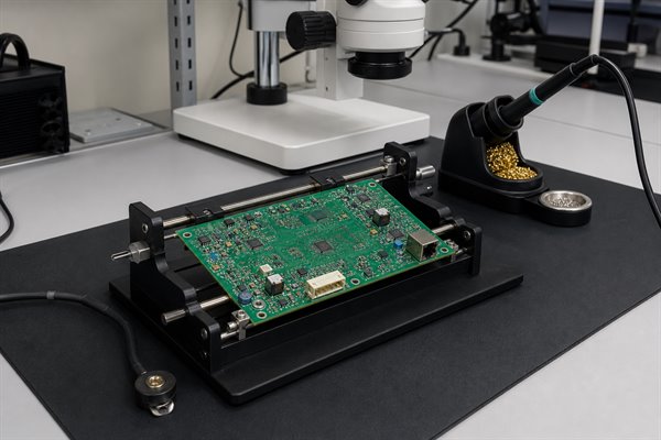
PCB and PCBA operations create repeated transitions between packaging, machines, fixtures, people, and test equipment. The control plan must cover the complete route rather than a single bench. Apply the controls at each production stage:
- Receiving and kitting: verify the ESD label and package condition before opening, then move parts to approved trays or containers. Keep moisture and ESD controls distinct because a moisture-barrier bag and an ESD shielding package may address different risks. Do not pour components into ordinary plastic bins or place cut tape on an uncontrolled surface.
- SMT preparation and manual assembly: include feeders, carts, racks, splice tools, setup benches, board supports, soldering equipment, and personnel grounding in the ESD assessment. Confirm the required controls before exposing components, and handle boards by their edges whenever the process permits.
- Repair and rework: define protected locations for replacement devices, removed components, suspect boards, and accepted boards. Keep microscopes, extraction equipment, fixtures, tools, and nearby materials within the control plan. A grounded operator cannot compensate for an ungrounded fixture or charged plastic beside the repair area.
- Inspection and testing: include fixtures, cables, probes, adapters, power supplies, and communication interfaces in the equipotential and verification strategy while maintaining electrical-safety requirements. Factory handling controls do not replace circuit-level immunity design; protection components, current paths, interfaces, layout, and product testing are covered separately in the guide to PCB ESD protection.
- Documentation and handoffs: keep assembly drawings, handling instructions, travelers, test procedures, packaging specifications, and nonconformance records consistent about item classification and required controls. Within the broader PCB manufacturing and assembly process, specify ESD handling at every transfer point instead of treating it as a final packing step.
How Should ESD-Sensitive Parts Be Stored and Transported?
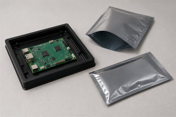
Outside an ESD-protected area, closed protective packaging is the primary defense. Select it for the journey and the product’s sensitivity, not by bag color or a generic “antistatic” label.
- Match protection to the route: Internal movement, warehouse storage, and commercial shipment expose a board to different people, surfaces, fields, and mechanical loads. Specify the needed combination of low charge generation, dissipation, and shielding for each route.
- Close before crossing the boundary: Seal the bag or container while still inside the approved handling location. An open bag beside a board provides no dependable shielding during movement.
- Inspect before reuse: Reject bags, foam, trays, or totes with punctures, contamination, worn surfaces, broken closures, or uncertain material identity. Preserve labels and lot or serial traceability.
- Control both opening and repacking: At receiving, move the closed package to an approved location before opening it. At final packing, immobilize the board, protect exposed connectors, and prevent accessories or documents from compromising the protective layer.
Ordinary bubble wrap, household bags, and loose foam should not contact exposed ESD-sensitive parts unless their suitability has been established. The protection remains effective only while its specified functions and closure stay intact.
How Do You Test and Maintain an ESD Control Program?
An ESD program is a maintained control system, not a one-time workstation purchase. Effective factory protection combines environmental controls, personnel training, and ongoing management. Use the following six steps to keep the program measurable and effective:
- Define the control plan and acceptance limits: identify which components and assemblies are ESD-sensitive, where they may be exposed, who owns each control, and which test method applies. The plan should cover protected-area boundaries, personnel grounding, work surfaces, floors, ionizers, tools, packaging, training, records, and corrective action. A device or workstation cannot be judged as passing unless the applicable limit and test method are defined before measurement.
- Perform operator checks before handling begins: test wrist straps, footwear systems, or continuous monitors at the frequency required by the plan. Confirm that cords, bands, ground connections, alarms, and workstation status are usable before opening protective packaging. Record a failed check and prevent the person or station from handling exposed ESDS items until the required control passes.
- Schedule measurements for fixed and process equipment: measure work surfaces, floors, carts, racks, fixtures, soldering equipment, and other control items according to their risk and qualification method. Check ionizers at the actual use position for the required balance and charge-decay performance. Repeat verification after relocation, repair, maintenance, material substitution, or a process change that could alter the grounding path or electrostatic field.
- Control instruments and retain usable records: use equipment suitable for the measurement range and keep its calibration or verification status current. Each record should identify the item, location, method, instrument, environmental conditions when relevant, result, acceptance limit, date, and person performing the check. A simple pass mark without the measured result or applicable limit is weak evidence when a failure must be investigated later.
- Audit the complete material flow: extend ESD training and auditing to receiving, storage, kitting, assembly, rework, inspection, testing, packaging, laboratories, and field activities. Observe actual transfers instead of reviewing documents alone. Confirm that visitors and temporary personnel follow access rules, protective packaging remains closed outside ESD-protected areas, and trained personnel know how to respond when a control fails.
- Contain failures and verify corrective action: stop exposing sensitive items where a required control has failed, identify the time window and material that may have been affected, and restore the control. Evaluate affected products using the approved disposition process rather than assuming that a normal visual or functional check proves no damage. Record the cause, correction, responsible owner, due date, and recheck result before closing the issue.
What ESD Prevention Checklist Should You Follow?
Use this concise checklist before touching or moving ESD-sensitive electronics:
- Confirm sensitivity: identify the item as ESD-sensitive and read its handling requirements.
- Keep packaging closed: do not open the protective package before it reaches the approved work area.
- Remove charge generators: clear ordinary plastic, foam, tape, and other unnecessary materials.
- Verify the grounding path: check both the workstation ground and the required personnel grounding system.
- Use approved controls: select suitable work surfaces, tools, fixtures, trays, and containers.
- Control insulators: remove nonessential insulators or neutralize essential ones with verified ionization.
- Handle by safe edges: avoid contacts, leads, pads, and test points on components and boards.
- Protect every operation: maintain ESD controls during assembly, rework, inspection, and testing, not only during soldering.
- Package before movement: close suitable protective packaging before storage or transport outside the controlled area.
- Stop after a failed check: record the result and do not continue while a critical control is out of specification.
- Investigate suspected exposure: review damaged packaging or uncontrolled transfers before releasing affected material.
- Review and reverify: audit the complete process periodically and confirm corrective actions after changes.
A practical summary of how to prevent ESD electrostatic discharge in electronics follows six actions. Identify sensitivity, control the area, ground conductors, neutralize essential insulators, protect the item during movement, and verify every safeguard. Skipping one of these actions can leave sensitive hardware exposed.
FAQs About Preventing Electrostatic Discharge (ESD)
Q1: Can a powered-off component still be damaged by ESD?
A1: Yes, powered-off components remain vulnerable to ESD. Removing operating power does not protect semiconductor junctions or exposed contacts. Apply the same handling precautions to powered-off parts and unpowered assemblies.
Q2: Do disposable nitrile gloves replace ESD grounding?
A2: No, ordinary nitrile gloves do not provide a verified grounding path. Gloves may also affect charge generation, so use them only when the process requires them and retain the approved personnel-grounding method.
Q3: Is a wooden workbench safe for ESD-sensitive electronics?
A3: A wooden bench is not ESD-safe by default. Its electrical behavior changes with coatings, contamination, wear, and humidity. Use a qualified ESD work surface with a defined ground path and measurement limits.
Q4: Can ESD damage be repaired?
A4: Latent ESD damage can be difficult to locate or prove absent. A failed component may sometimes be replaced, but suspect material should be quarantined and investigated under the product’s disposition procedure rather than released after only a quick functional test.
Q5: Can ESD shielding bags be reused?
A5: Reuse a shielding bag only when the approved procedure allows it. The bag must remain clean, identifiable, undamaged, and able to close correctly. Replace it after puncture, severe creasing, contamination, or uncertain history.
Q6: Can visitors enter an ESD-protected area?
A6: Visitors may enter only under the site’s controlled-access rules. They may need training or an escort, the same personnel-grounding checks as operators, and restrictions on personal items and clothing.
Q7: Can batteries or powered assemblies go into conductive packaging?
A7: Do not select packaging by ESD properties alone. Exposed energy sources can create a short-circuit or safety hazard, so follow the product-specific packaging method and insulate terminals where required.
Q8: What should happen after a continuous monitor alarm?
A8: Stop exposing sensitive hardware immediately. Protect or close the material, identify the failed connection or equipment, record potentially affected work, and resume only after the system passes verification.
Q9: Who should own an ESD control program?
A9: Assign a named ESD coordinator and accountable process owners. Responsibilities should cover production, maintenance, quality, training, and corrective action because failures often cross departmental boundaries.
Q10: When should an ESD risk assessment be repeated?
A10: Reassess ESD risk before a changed process becomes routine. Repeat the assessment after changes to products, layouts, materials, equipment, packaging, environmental conditions, or handling routes, and after unexplained failures.
Conclusion
Preventing ESD in electronics requires more than avoiding visible sparks. Effective protection starts before a package is opened and continues through assembly, repair, testing, storage, and transport. Ground conductors and personnel through approved systems. Neutralize charge on essential insulators, protect exposed hardware outside controlled areas, and correct failed checks before work resumes.
Need reliable PCB fabrication or assembly support with clearly defined ESD handling requirements? Contact EBest Circuit and send your Gerber/ODB++, BOM, quantity, stackup, assembly, programming, and test requirements to sales@bestpcbs.com.