When one of two parallel MOSFETs runs hotter, do not start by adding more copper or changing the gate resistor. First measure the two branch currents during the flat part of the on-time, then compare the switching edges. A mismatch on the plateau points first to the fully enhanced resistance and power paths. A mismatch confined to the edges points first to gate drive, commutation inductance, or device timing. If current and switching losses are similar, look at the two thermal paths instead.

MOSFETs in Parallel: When It Pays Off
Parallel MOSFETs share the drain and source nodes of one switch. Splitting current across two devices can lower conduction loss and spread heat. It also adds gate charge, layout area, and more opportunities for one branch to take a bigger share. It does not raise the voltage rating. Do not add two datasheet current ratings to obtain a board rating. If you are new to the device, start with this FET fundamentals guide.
Consider a 24 V motor driver that needs 40 A through the energized low-side switch position. One device might meet the requirement with a stronger package or better thermal path. Two devices are justified if the single device cannot meet the loss or temperature budget, and if the layout and driver can support two independently verifiable branches. This example uses assumed values throughout, not test data.
Parallel MOSFET Current Sharing
In the 40 A example, effective branch resistances of 3 and 4 mΩ give 22.9 and 17.1 A, not 20 A each. This is the fully on, fixed-temperature limit. Both branches see the same terminal voltage, so the lower resistance draws more current: IA = Itotal × RB ÷ (RA + RB). Effective resistance includes the device and the separate copper, vias, solder joints and other interconnects between the common split and join points. Shared copper before the split does not enter this simple division.
At a switching edge, that equation is not enough. The first MOSFET to turn on can momentarily carry most of the load, even when the later plateau is nearly balanced. A device that turns off later can take disproportionate turn-off energy. Check the plateau and edges separately rather than judging the current split from a single average value.
| Where the mismatch appears | First thing to check | What would confirm it? |
|---|---|---|
| Fully on, after the edge | Hot branch resistance and actual gate-to-source voltage | Separate millivolt measurements show a resistance difference large enough to explain the current split. |
| Turn-on or turn-off only | Local gate waveform and commutation path | A branch current peak lines up with a repeatable gate or drain waveform difference. |
| Temperature only | Heat flow into the board or heatsink | Electrical losses are similar, but the hotter device has a less effective thermal path. |
MOSFET On Resistance vs Temperature
Use the expected hot RDS(on) at the actual gate drive, not the headline room-temperature typical value. For the example, suppose the two device contributions are 2.5 and 3.2 mΩ, with the remainder in the respective interconnects. Using the currents above, device-only conduction losses are approximately 1.31 and 0.94 W during the on-state. For steady PWM plateaus, multiply by on-duty fraction as a first estimate; it excludes switching and reverse-conduction losses. The branch that takes 5.8 A more is not necessarily the branch with the worst junction temperature; heat removal still matters.
A fully enhanced silicon MOSFET often has increasing on-resistance with temperature, which helps steady sharing. Verify the curve for the selected part. Do not assume the same stabilizing effect while the device is only partly enhanced, such as during slow startup or linear current limiting. Check the time-dependent safe operating area for those conditions; a low on-resistance does not qualify a device for linear operation.
Parallel MOSFET PCB Layout
Start by tracing the two drain paths from the common node to the packages and the two source paths back to the common return. Match path resistance and inductance, not just trace length. Layer changes, via arrays, plane neckdowns and unequal pad entry can make two equal-length paths electrically different. Where one device is fed through the other device’s connection point, move the split so each receives a comparable path. Keep the gate loop and the high-current commutation loop short and check both.
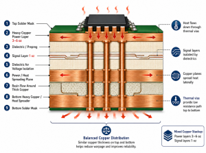
For heavy copper, note the finished thickness by layer instead of relying on a nominal ounce designation. Check actual copper at narrowed pads and via transitions, and account for the copper that connects the switch to the local bus capacitor. IPC-2152 addresses copper conductor sizing and temperature rise. It does not prescribe a current-sharing tolerance between devices or certify the full assembly. For the 40 A board, compare four-wire branch drops on the sample and verify temperatures with the actual cooling conditions.
Parallel MOSFET Gate Resistor
Place a separate local series gate resistor at each MOSFET. A single resistor ahead of the branch point limits the overall drive, but does not provide the same damping between the individual gate loops. Start with equal, manufacturer-informed values and comparable gate paths. If one branch switches faster, investigate source bounce and layout before trying to cancel it with different resistors.
A larger gate resistor can reduce ringing and overshoot, but slower edges can increase switching loss. On the example board, adjust one design variable at a time and compare overshoot, branch current peaks and switching loss under the same conditions. Fixing the visible ringing alone is not enough if the switch then exceeds its thermal budget at the actual switching frequency.
Kelvin Source MOSFET: When the Sense Pin Helps
A Kelvin source pin gives the driver a separate source reference. In a three-terminal layout, the same source path often carries gate-return current and power current. A rapid change in the latter produces a voltage across the shared inductance, so the effective gate-to-source voltage at the die can differ from what a driver-side trace suggests.
For a package with a dedicated sense source, route the drive return according to the manufacturer’s recommendation. Do not divert load current into that pin. With a three-terminal package, a separate board return to the source pad can remove some shared PCB impedance, but it cannot remove shared inductance inside the package. Compare gate voltage at the device references before and after the layout change.
Parallel MOSFET Gate Driver
The driver must charge and discharge both gates. For two assumed 45 nC devices at 100 kHz, the mean charge drawn for the pair is about 9 mA per switch position. This is a switching-charge estimate, not a peak-drive specification. Select using the actual datasheet gate-charge conditions and account for driver output resistance, the Miller plateau, thermal limits and the required transition time.
| Option | When to use it | What it costs or leaves to verify |
|---|---|---|
| One larger MOSFET | One package meets the conduction, switching and cooling targets. | Simpler drive and measurement, but heat is concentrated in one package. |
| Two discrete MOSFETs | There is room for matched branches and cooling, and the driver can handle both gates. | More gate charge and routing. Verify each branch at hot load and during edges. |
| Power module | A documented module construction fits the current and mechanical envelope. | Higher integration does not remove external bus or cooling limits. Check its terminal and mounting conditions. |
Double Pulse Test Setup
A double-pulse test places a controlled load current in the inductive test circuit, then uses the switching events to reveal overshoot, ringing and switching energy. For a parallel pair, total current alone can hide one overloaded branch. Use repeatable, suitable voltage and branch-current sensing, confirm probe bandwidth and timing alignment, and check that the sensor does not add enough impedance to change the split. Follow the instrument and fixture safety requirements; measurements on energized power stages belong in a qualified lab.
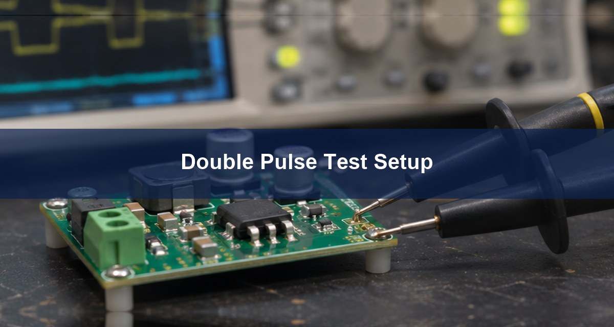
For the 40 A design, establish separate acceptance limits before testing: plateau current per device, peak branch current, VDS and VGS excursions, loss and junction-temperature margin. Document the bus voltage, temperature, load, device lot, gate settings and probe positions. Compare cold and hot results, then run continuous PWM in the real assembly: a double pulse does not establish sustained thermal performance. Keep the PCB revision, finished copper specification and the test report together. If the heavy-copper stackup changes, recheck the measured branch balance rather than assuming that equal trace widths preserve it.
FAQ
Can MOSFETs in parallel double the current rating?
No. The circuit is limited by the more heavily loaded branch, its switching and temperature, and the board and cooling constraints.
Can two parallel MOSFETs use one gate resistor?
They can switch with a common resistor, but it does not give each gate loop local damping. Start with a resistor per device and verify the waveforms.
Why does one MOSFET run hotter at the same measured DC current?
Compare switching losses, hot on-resistance and the path into the board or heatsink. Equal mean current does not imply equal dissipation or equal temperature.
Does increasing the gate resistance cure drain overshoot?
It may reduce the switching slew rate, but overshoot can also come from the commutation loop or the measurement setup. Verify those first and retest losses after the change.
Does a Kelvin source pin make both branches equal?
No. It reduces common-source feedback in the gate loop; it does not correct differences in power paths or device parameters.
Can a thermal camera prove current is sharing?
No. Use it to locate hot areas, but compare electrical waveforms and account for surface emissivity and thermal paths. Case temperature is not junction temperature.
Can a sample pass a double pulse test and still overheat?
Yes. The test isolates switching events and does not establish continuous operating temperature. Run the assembled board at sustained duty, temperature and cooling conditions.
Can a second-source MOSFET be mixed into a parallel pair?
Only after comparing the exact part’s on-resistance versus temperature, gate charge, threshold spread, switching behavior, package and thermal conditions, then verifying the populated board. Similar headline resistance does not establish compatibility.
References
- Nexperia IAN50005: Paralleling power MOSFETs in high power applications
- Texas Instruments SLPA020: Driving Parallel MOSFETs
- Tektronix: Double Pulse Testing Application Note
Discuss a High-Current PCB Layout
For a heavy copper PCB fabrication review with Best Technology, send the board revision, stackup, finished copper requirements, via arrays and the test points used to compare the two branches to sales@bestpcbs.com. Start with the path that must preserve the validated voltage drop or temperature margin.