SCD21 measures how much of a differential stimulus at logical port 1 emerges as common mode at logical port 2. On a PCB pair, skew, unequal losses or unequal transitions can contribute. First confirm the port mapping and fixture response; otherwise the test setup can look like a layout problem.
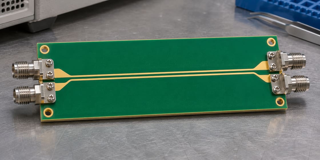
How to read the letters and port numbers
The output mode comes first and the input mode second: C is common, D is differential. The 21 identifies output at logical port 2 with stimulus at logical port 1. Keysight’s balanced-measurement reference explains this convention.
What to capture with a plot
Record the data needed to repeat the comparison.
| Parameter | Unit or definition | Check |
| Sweep | Hz and points | Same band and frequency grid |
| Logical port mapping | Two conductors per end, with polarity | Matches the physical fixture and file order |
| Reference impedances | Ω, including normalization | Same convention for compared traces |
| Calibration planes | Physical locations | Same fixture inclusion or removal |
| Reported response | dB versus frequency | Compare the correct term and direction |
SCD21 vs SDD21 vs SDC21
These terms describe different input and output modes.
| Term | Input and output | What it tells you |
| SCD21 | Differential in, common out | Forward differential-to-common conversion |
| SDD21 | Differential in, differential out | Forward differential transmission |
| SDC21 | Common in, differential out | Forward common-to-differential conversion |
Use a skew example as a diagnostic clue
In an ideal equal-loss, uncoupled pair with otherwise identical matched paths, delay mismatch alone produces a converted magnitude of |sin(πfΔt)| relative to the incident normalized differential wave for lossless paths. At 5 GHz and 5 ps, this is about 0.0785, or −22.1 dB. This is a simplified example, not a channel acceptance limit or a way to infer skew from every measured trace.
Check unequal amplitude as well as delay
If the two paths deliver different amplitudes, they do not cancel perfectly in the common-mode sum even with equal delay. Compare individual path responses before adding length. Equal drawn trace length cannot fix a connector or launch that attenuates one conductor more.
Verify the physical port map first
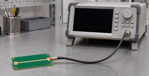
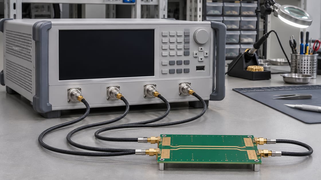
Map the two conductors at each end to the analyzer’s logical pairs. A swapped port or polarity can alter the interpretation of a mixed-mode plot. Preserve the port map with the raw single-ended S-parameter file so the conversion can be repeated.
Establish the fixture baseline
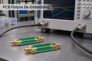
Compare a known balanced reference or verification coupon with the DUT. Verify repeatability and the calibration planes before attributing a conversion peak to the board. For related measurement boundaries, see the PCB fixture de-embedding guide.
Inspect asymmetry where the pair changes geometry
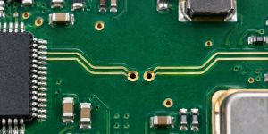
Compare both launches, vias, reference transitions and termination areas. For example, one conductor may encounter a different pad or return path near a layer change. Check the structure at the same point on both sides instead of assuming the straight runs are the only source.
Interpret broad trends and narrow peaks differently
A gradual increase can be consistent with simple delay mismatch over a limited band. A narrow peak may suggest a discontinuity, resonance or fixture effect. Neither shape alone identifies root cause. Compare changes between controlled layout or fixture variants.
Keep conversion and emissions evidence separate
Converted common mode can be relevant to emissions, but a conversion plot does not establish regulatory pass or fail. Coupling to cables, enclosure features and the operating stimulus also matter. Verify at the appropriate system level when emissions are the concern.
Use the product’s requirement, not a generic threshold
Set the allowable conversion over the specified band and reference planes using the actual system or interface requirement. Do not apply a rule from a different connector or application. Document the noise floor or repeatability limits near the acceptance boundary.
Deliver a reproducible comparison
Save the port map, stackup, fixture setup, raw data, conversion convention and limits with the plots. For a PCB or coupon manufacturing review, share those requirements with Best Technology at sales@bestpcbs.com.
FAQ
Does more-negative SCD21 usually mean less conversion?
Yes when comparing magnitude in dB under the same normalization and reference planes. A more-negative number represents a smaller converted wave relative to the input. Ensure the measured response is above the useful noise floor before drawing conclusions from small differences.
Can good insertion loss hide conversion?
A channel may have acceptable differential transmission and still generate common mode. Plot SDD21 and SCD21 as separate quantities across the same band. Check each against the appropriate requirement rather than relying on a single loss trace to characterize every response.
Can I read SCD21 from a single-ended two-port measurement?
Not from one ordinary two-port trace alone. The conversion depends on the responses of both conductors in each logical port under the applicable normalization. Use suitable multiport measurement data and record the port pairing and calculation convention used for the mixed-mode result.
Does zero skew guarantee zero mode conversion?
No. It removes one possible mechanism but does not eliminate amplitude imbalance or asymmetry in launches, return paths and terminations. Check the complete channel and fixture. Equal timing in one part of the path cannot establish balance at every discontinuity or frequency.
Can I use SCD21 to locate a fault by itself?
It can show where in frequency the conversion is observed, but not automatically where on the board it originates. Combine it with reference structures, controlled layout changes or suitable time-domain analysis. Verify the fixture before attributing the result to a specific feature.
Should I compare two plots with different reference planes?
Not as if they represent the same DUT. One may include a connector or launch that the other removes. Align the planes or explicitly describe the difference. Preserve the raw measurements so another engineer can reproduce the comparison under the intended convention.
Can a software port swap repair a real board problem?
It can correct a bookkeeping error if the measured ports were paired incorrectly, but it cannot change a real electromagnetic imbalance. Verify the physical assignment before reprocessing the data. If the conversion remains, check the fixture and compare equivalent features of both conductors.
Is there a universal pass limit for SCD21?
No. The acceptable magnitude depends on the interface, band and system requirement. Set the limit with defined reference planes and test conditions, and account for fixture repeatability. Do not transfer a limit from an unrelated assembly just because the two channels use similar impedance.