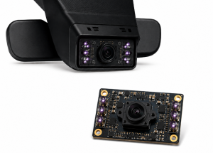
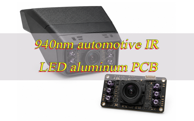
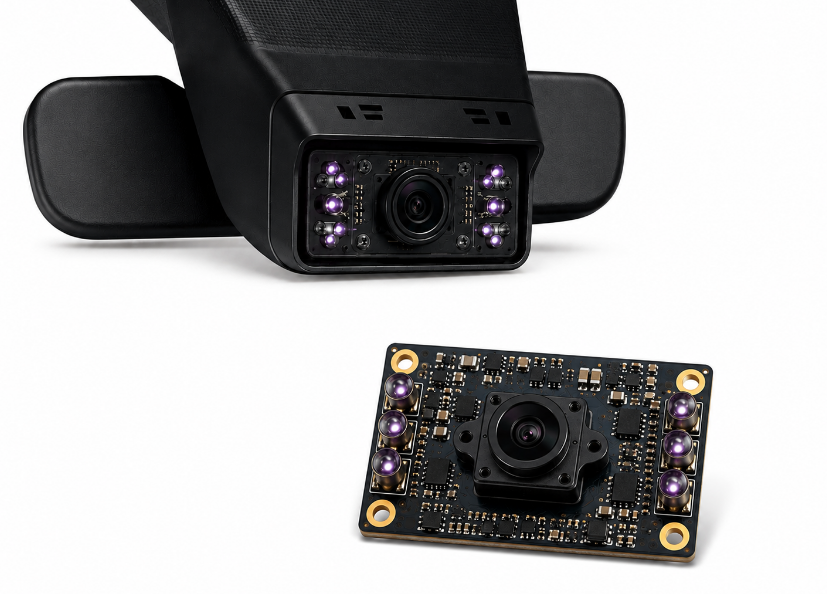
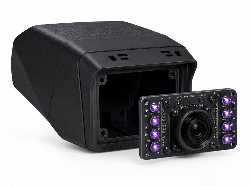
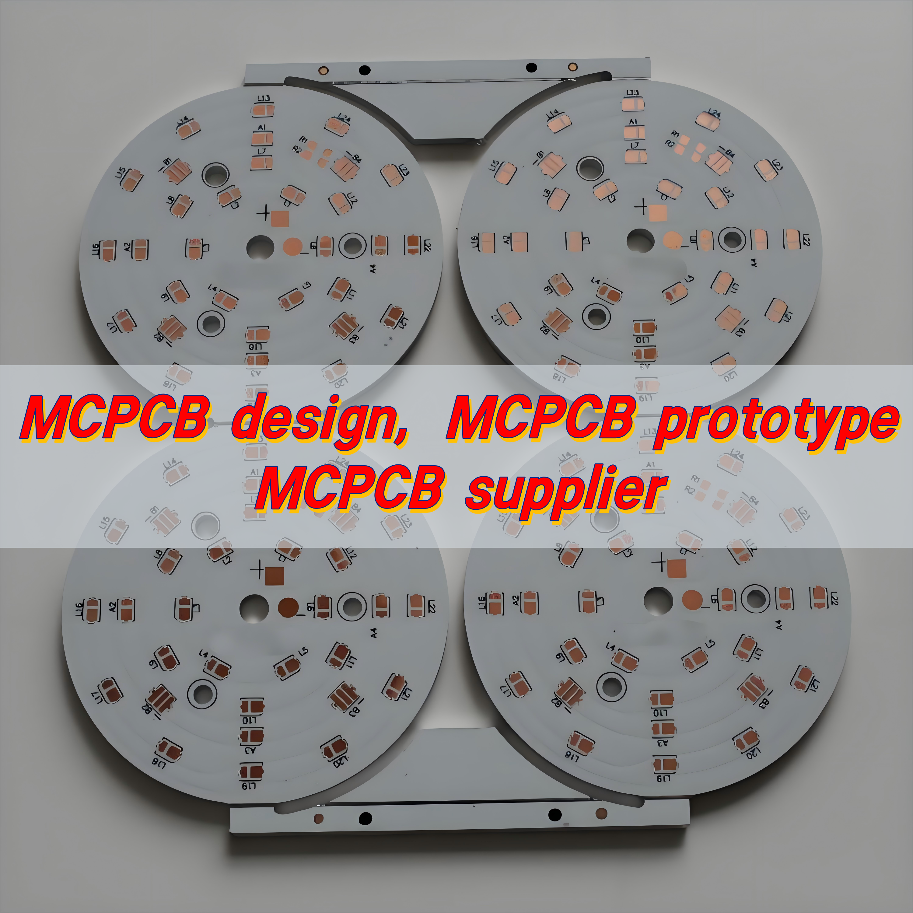
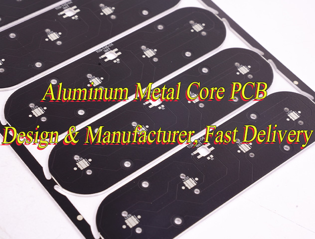
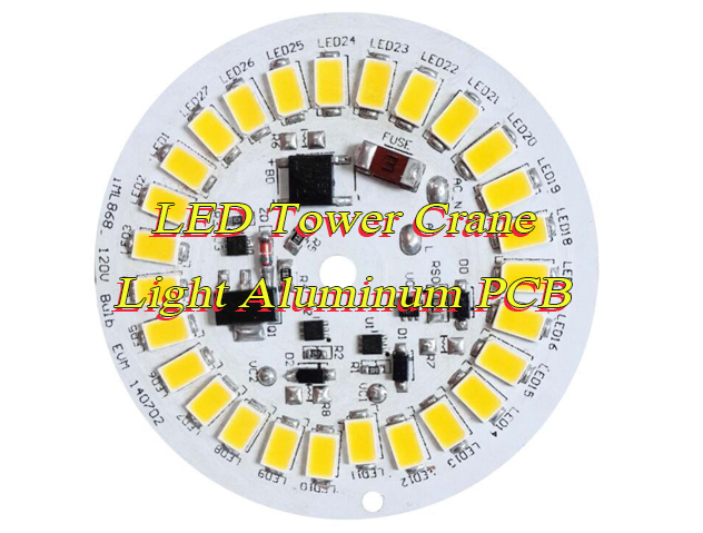
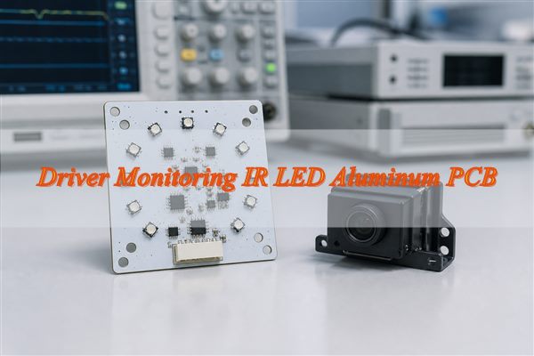
A driver monitoring IR LED aluminum PCB provides the near-infrared illumination that helps an automotive DMS camera capture the driver’s face and eyes in changing cabin light. For buyers, the right board is not simply an aluminum PCB populated with IR LEDs. Its optical position, pulse-current path, heat flow, camera compatibility, assembly controls, and verification plan must work as one module.
When the PCB manufacturer receives the pulse profile, LED data, mechanical drawing, optical datums, thermal limits, and test expectations before quotation, it can identify missing production inputs before they become tooling changes, assembly delays, or inconclusive prototype results.
Are you worried about your driver monitoring IR LED aluminum PCB project?
- Will uneven IR coverage leave the driver’s eyes underexposed at off-axis seat positions?
- Could pulse-current droop or trigger delay reduce usable illumination during camera exposure?
- Will an incomplete board-to-housing heat path raise LED temperature during repeated pulses?
With over 20 years of experience, EBest Circuit provides one-stop PCB and PCBA manufacturing support from prototype review through production.
- Optical datum review: We check LED position, rotation, board outline, and mounting references against the supplied camera and housing drawings before fabrication.
- Pulse-path review: We review the supplied peak current, pulse width, trigger timing, copper path, return path, and assembly inputs before prototype release.
- Thermal-interface review: We check the specified aluminum construction, dielectric, board flatness, mounting pattern, and housing-contact requirements against the released manufacturing package.
Ready to start your driver monitoring IR LED aluminum PCB project? Send your files and requirements to sales@bestpcbs.com.
What Does a Driver Monitoring IR LED Aluminum PCB Do in an Automotive DMS?
A driver monitoring IR LED aluminum PCB supports the IR emitters electrically, thermally, and mechanically so the DMS camera can obtain usable images of the driver. The board carries pulse current to the LEDs, transfers heat toward the aluminum base and housing, and holds the emitters at controlled locations relative to the camera and lens.
A driver monitoring system IR LED board therefore sits at the intersection of several project teams. The electronics team defines current and timing. The optical team defines wavelength, beam shape, coverage, and camera alignment. Mechanical engineers control the board position and heat-transfer interfaces. Manufacturing and quality teams convert those inputs into repeatable assembly and acceptance evidence.
| Project Input | PCB or PCBA Decision | Business Risk If Missing |
| Camera exposure timing | Pulse trigger and current-delivery requirements | Prototype images may be too dark, inconsistent, or affected by switching |
| LED electrical and thermal data | Driver headroom, copper path, dielectric, and heat path | Redesign after component selection or thermal testing |
| Optical and mechanical datums | LED footprint position, board outline, and assembly orientation | Illumination may miss the required face or eye region |
| Vehicle and customer requirements | Materials, controls, traceability, and test planning | Quotation may exclude required verification or documentation |
Use this matrix to assign each missing input to the responsible team before quotation. Camera timing belongs with the electronics and imaging teams, optical datums with optical and mechanical engineering, and verification records with the customer, module owner, and supplier according to the agreed scope.
How Do IR LEDs Provide Consistent Illumination Across the Driver’s Face and Eyes?
Consistent illumination comes from coordinating LED position, emission angle, lens behavior, camera axis, and the expected driver-position range. Increasing LED power cannot correct a beam that is aimed at the wrong region or blocked by the steering wheel, trim, or eyewear reflections.
For an automotive DMS IR illuminator, the PCB drawing should identify optical and mechanical datums rather than relying only on the board outline. LED pad locations, polarity, rotational orientation, component height, and permitted placement variation can all influence the final beam. The optical validation plan should also include realistic driver positions, eyeglasses or sunglasses where applicable, and the actual camera-lens stack.
- Define the coverage zone: specify the face and eye region at the required seat travel, seat height, steering-wheel position, and driver posture. This prevents the optical target from being reduced to one nominal head position.
- Lock optical datums: dimension LED centers and rotation from mounting features that also locate the camera, lens, PCB, and housing. Board-edge tolerances are insufficient when the enclosure uses different functional references.
- Match the beam to the FOV: compare the LED radiation pattern and any secondary optics with the camera field of view. Overly wide illumination wastes current outside the captured region; a narrow or misaligned beam creates dark areas as the driver moves.
- Review obstruction and reflection risks: evaluate trim, steering-wheel position, eyeglasses, sunglasses, bright facial reflections, and off-axis viewing. These conditions can hide the eyes even when total scene brightness appears adequate.
- Validate the assembled module: capture images through the production-intent lens, filter, cover window, and housing across the required driver positions. A bare-board radiometric measurement cannot establish image uniformity after the optical stack is installed.
Record both the operating condition and the image result. LED current, exposure, ambient light, seat position, eyewear, and module temperature should be traceable to each validation image so that an optical problem can be separated from a timing, thermal, or assembly change.
How Are IR LED Pulses Synchronized with DMS Camera Exposure?
Use the camera’s exposure or strobe signal to command the LED driver, then place the full IR current pulse inside the pixels’ light-collection period. The timing budget must include trigger propagation, driver turn-on delay, current rise and fall time, and worst-case tolerance. If either edge falls outside the exposure interval, part of the optical pulse produces heat without contributing to the captured image.
Shutter type changes the synchronization decision. A global-shutter sensor exposes all pixels together, so one pulse can cover the shared exposure interval. A rolling-shutter sensor exposes rows at different times; a short pulse may illuminate only part of the frame unless the sensor provides a supported strobe mode or the pulse covers the required row sequence. Confirm the method in the selected image-sensor documentation before fixing the PCB trigger interface.
| Timing Check | What to Establish | Failure Visible in the DMS Image |
| Trigger reference | Which camera or controller edge starts the illumination command | Pulse occurs in the wrong frame or at an inconsistent phase |
| Driver delay | Delay from the logic command to stable LED current, including tolerance | Reduced effective illumination or frame-to-frame brightness change |
| Pulse window | Start and end margins inside the applicable global or rolling exposure period | Dark rows, uneven exposure, or wasted on-time |
| Repetition behavior | Current recovery and timing stability across the required frame sequence | Brightness changes during consecutive frames |
| Fault limit | Maximum on-time and the shutdown response if the trigger remains active | Excess heat or optical output outside the intended operating state |
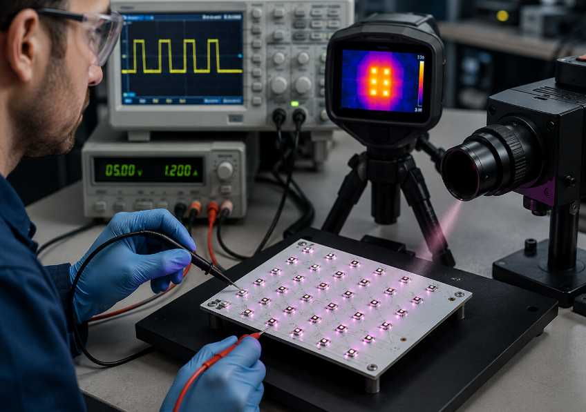
During prototype validation, observe the trigger and LED current on the same time base while the camera captures images. Repeat the check at the specified supply and temperature limits; a waveform that aligns at room temperature alone does not establish the available timing margin.
How Does the PCB Handle High Peak Current During IR LED Pulses?
The PCB must deliver the specified peak current without excessive voltage drop, unstable driver operation, or unwanted disturbance elsewhere in the module. This depends on the complete current loop, not only the nominal copper thickness.
The design review should follow current from the local energy source through the driver, LED string, return path, and decoupling network. Trace geometry, copper weight, connection transitions, component placement, voltage headroom, and recharge time all affect the result. The driver and LED datasheets remain the authority for component limits; the PCB supplier should not replace missing electrical specifications with assumed universal values.
| Review Item | Decision Needed | Evidence for Prototype Approval |
| Pulse profile | Peak current, width, frequency, duty cycle, and tolerance | Measured waveform at the defined operating condition |
| Voltage headroom | Supply range, LED string voltage, driver losses, and transient margin | Waveform remains within selected component limits |
| Current loop | Short routing, return continuity, connections, and local storage | No unexpected droop, overshoot, or unstable pulse shape |
| Recharge interval | Energy replenishment before the next exposure | Repeated pulses remain consistent over the required sequence |
Release the pulse-current design for prototype testing only after the measured waveform confirms the required peak current, timing, voltage headroom, and recovery between exposures. If one result is outside its limit, correct the current loop or operating specification before using thermal or optical results as approval evidence.
How Is Heat Controlled for Pulsed IR LEDs on an Aluminum PCB?
Thermal control requires a continuous heat path from the LED junction through the package, PCB, aluminum base, interface material, and housing. An aluminum substrate helps spread heat, but it does not by itself prove an acceptable junction temperature or service life.
Peak LED power affects the temperature rise during each pulse, while duty cycle, repetition rate, driver losses, ambient temperature, and the module’s thermal time constants determine accumulated heating. Review peak conditions for component limits and average dissipation for the sustained thermal state; using only one of them can hide a different failure mode.
- Start with the real pulse profile: use LED forward voltage, peak current, pulse width, repetition rate, and worst permitted on-time. Include driver and resistor losses when they share the same board and heat path.
- Review the dielectric layer: thermal conductivity and dielectric thickness act together. A high-conductivity material can still create excessive thermal resistance if the construction or bond line is too thick for the required heat flow.
- Spread heat before the bottleneck: size LED pads and connected copper so heat reaches the dielectric over a practical area. Narrow copper necks can limit spreading before heat reaches the aluminum base.
- Complete the housing interface: define board flatness, mounting pressure, interface material, contact area, fastener pattern, and housing surface. Air gaps or uneven contact can dominate the module result even when the PCB construction is correct.
- Check the hottest operating case: combine the highest permitted ambient, pulse sequence, enclosure condition, and heat from nearby components. Test the location expected to run hottest rather than relying on a convenient board-edge measurement.
Prototype approval should link a temperature measurement at a defined location to the LED junction through the package manufacturer’s thermal data and an agreed calculation or model. Record the ambient condition, pulse sequence, stabilization time, sensor position, interface assembly, and acceptance limit. External board temperature alone does not prove junction temperature, optical-output stability, or LED life.
How Does PCB Layout Prevent Switching Noise from Affecting the DMS Camera?
Layout reduces interference by shrinking fast-current loops, controlling return paths, and separating switching nodes from sensitive camera and data circuits. Filtering cannot fully compensate for poor current-loop geometry.
- Close the pulse-current loop: place the driver, local energy-storage capacitor, LED connection, current-sense element, and power return close enough to avoid a large high-di/dt loop. Long paths increase voltage disturbance and radiated coupling.
- Control the switching-node area: keep high-dv/dt copper no larger than required and away from camera, clock, trigger, and communication routing. Do not route sensitive traces under or beside an exposed switching region without an intentional reference structure.
- Preserve return continuity: provide a defined path for pulse current and a stable reference for camera and data signals. A split or narrow return path can force current through a shared reference and convert switching current into image or communication noise.
- Place filtering at the disturbance boundary: locate local decoupling at the driver and any interface filtering where power or signals enter the sensitive region. A filter placed after a long noisy trace leaves the coupling path intact.
- Protect trigger integrity: route the exposure or strobe signal away from the power switch node, control its return path, and check logic thresholds at the receiving pin. Trigger jitter or false edges can look like an optical-timing problem.
- Balance edge rate and optical timing: slew-rate control may reduce emissions, but a slower current edge consumes timing margin and can reduce useful optical energy during a short exposure. Verify both waveform quality and captured images after changing the edge rate.
PCB review can identify layout risk, but vehicle EMC compliance requires the applicable module and vehicle tests. During prototype work, monitor electrical emissions, trigger integrity, data communication, and camera images under the same representative pulse modes; a continuity test cannot reveal exposure-related coupling.
What Automotive Design Requirements Must Be Defined Before Layout Begins?
The project should define electrical, environmental, optical-safety, mechanical, quality, and traceability requirements before the PCB is released. This prevents a supplier from quoting a board that is manufacturable but incomplete for the intended automotive module.
- Electrical envelope: document normal and abnormal supply conditions, pulse-current limits, trigger logic, load-dump or transient protection ownership, reverse-polarity strategy, and fault shutdown behavior. Identify which protections are on the illuminator board and which remain elsewhere in the module.
- Environmental conditions: define operating and storage temperature ranges, temperature ramp or cycling conditions, vibration, mechanical shock, humidity or condensation exposure, coating needs, and installation loads. Connect each condition to the required board material, component grade, attachment method, or validation owner.
- Optical-safety boundary: assign responsibility for the exposure assessment and provide wavelength, radiant-output data, pulse current, pulse width, repetition rate, lens or diffuser behavior, viewing geometry, and fault-state on-time. A component rating cannot replace the assembled optical-system assessment.
- Mechanical interface: release the mounting datums, board outline, keep-outs, connector location, allowed warpage, housing contact area, interface material, fastener constraints, and permissible component height. These inputs control both optical alignment and the heat path.
- Quality and change control: state applicable customer specifications, workmanship criteria, approved component sources, substitution rules, first-article expectations, process-change notification, lot traceability, retention period, and required reports.
- Verification ownership: identify what is accepted by component documentation, bare-board inspection, assembled-PCB test, optical-module validation, EMC testing, environmental testing, and vehicle approval. Assign the pass criterion and evidence owner for each level before purchase-order release.
Convert the requirements into a responsibility matrix with four fields: requirement, applicable condition, acceptance evidence, and responsible organization. Request certification or material declarations by exact scope. A supplier management-system certificate, a material listing, a component rating, and a finished-module compliance result are different evidence types and cannot substitute for one another.
How Is a DMS IR LED Aluminum PCB Manufactured and Assembled?
Production should preserve the electrical, thermal, optical, and polarity decisions established during design review. The build route therefore needs controlled material identity, PCB fabrication, component orientation, reflow, cleaning, and traceability rather than a generic aluminum-board process description.
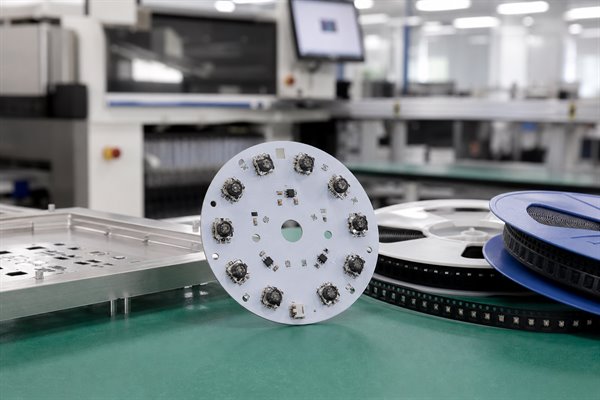
- Confirm production inputs: release the approved fabrication data, stackup, aluminum and dielectric requirements, BOM, centroid file, polarity drawing, optical datums, panel requirements, and acceptance plan; record unresolved discrepancies before tooling.
- Verify incoming materials: match laminate, dielectric construction, aluminum base, copper, surface finish inputs, LEDs, drivers, and assembly materials to the released documentation; quarantine mismatches to prevent an unapproved substitution.
- Fabricate the PCB: image and etch the circuit, process the metal-core construction, drill or route required features, apply solder mask and surface finish, and control the board outline and datum features needed by the housing.
- Prepare solder paste: use the approved stencil and printing setup for the selected LED and driver packages; inspect deposits where solder volume can affect coplanarity, thermal contact, or bridging risk.
- Place components: load the released program and verify LED polarity, rotation, package identity, and datum-related placement before the batch proceeds to reflow.
- Reflow and clean: use a profile compatible with the components, PCB construction, solder paste, and product requirements; review for package movement, void-related concerns where specified, contamination, and visible heat damage.
- Depanel and identify: separate boards without damaging the aluminum structure or critical edges, then preserve lot and material traceability through inspection and shipment.
Build prototypes with the intended production materials and assembly orientation. If a temporary component or process is unavoidable, document the difference so the prototype result is not mistaken for production validation.
How Is a Driver Monitoring IR LED Aluminum PCB Inspected and Tested?
Inspection should produce evidence that the delivered board matches the released design and performs under the agreed test conditions. The plan should distinguish bare-board, assembled-board, module, and vehicle-level responsibilities.
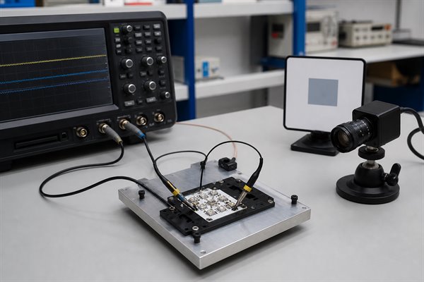
- Inspect the bare board: verify dimensions and specified datums, visual workmanship, electrical continuity and isolation, and the agreed material or traceability records; disposition deviations against the released drawing.
- Inspect the assembly: confirm component identity, polarity, rotation, placement, solder joints, cleanliness, and mechanical condition using the agreed visual, AOI, or other inspection methods.
- Measure the pulse: operate the assembly at defined supply and trigger conditions, measure current and relevant node waveforms, and compare peak value, width, timing, droop, and overshoot with approved limits.
- Check thermal behavior: run the stated pulse sequence and ambient condition, measure at documented locations, and compare results with the project limit and junction-temperature assessment method.
- Verify optical alignment: install the board in the representative optical-mechanical stack, capture camera output across the required driver positions, and assess coverage, reflections, and image consistency against system criteria.
- Evaluate interference: operate worst-case pulse modes while monitoring camera images and data communication; escalate abnormal artifacts or errors for module-level EMC investigation.
- Release the evidence: link results, nonconformance dispositions, lot identity, and approved deviations to the shipped samples or production batch so procurement can audit what was actually accepted.
What Should You Send for a DMS IR LED Aluminum PCB Quote?
The quotation package must define the board, assembly, control, and verification scope to be priced. Sending only Gerber files and quantity may produce a preliminary board price, but it cannot define optical alignment, pulse testing, component sourcing, or automotive documentation.
- PCB data: Gerber or ODB++, drill files, outline, drawing, stackup, copper, dielectric, aluminum-base, surface-finish, and panel requirements.
- Assembly data: BOM with manufacturer part numbers, centroid file, drawings, LED polarity and rotation, acceptable substitutions, and special handling needs.
- System interfaces: camera and trigger information, pulse profile, supply range, connector details, optical datums, housing interface, and thermal limits.
- Quality scope: inspection criteria, test limits, sample size, traceability, reports, customer specifications, and required declarations.
- Commercial scope: prototype and production quantities, target schedule, delivery destination, packaging, and whether component sourcing or turnkey PCB assembly is required.
If some inputs are not yet frozen, identify them as open items. An early design review can separate information needed for budgetary pricing from information required before fabrication, assembly, or test release.
Why Choose EBest Circuit for Driver Monitoring IR LED Aluminum PCB Manufacturing?
EBest Circuit can support the project from PCB design review and prototyping through component sourcing, PCB assembly, and mass production.
Our supplied company information identifies metal-core PCB capability and services covering PCB design, PCB prototypes, mass production, component sourcing, and PCB assembly. It also lists an IATF 16949 certification within the company’s certification inventory. Certification relevance and document scope should be confirmed for the specific purchasing requirement rather than treated as automatic product approval.
- Design-to-production continuity: review stackup, footprint, polarity, panel, sourcing, assembly, and test inputs before tooling. The same controlled package can then be updated through prototype findings instead of recreating requirements for each supplier handoff.
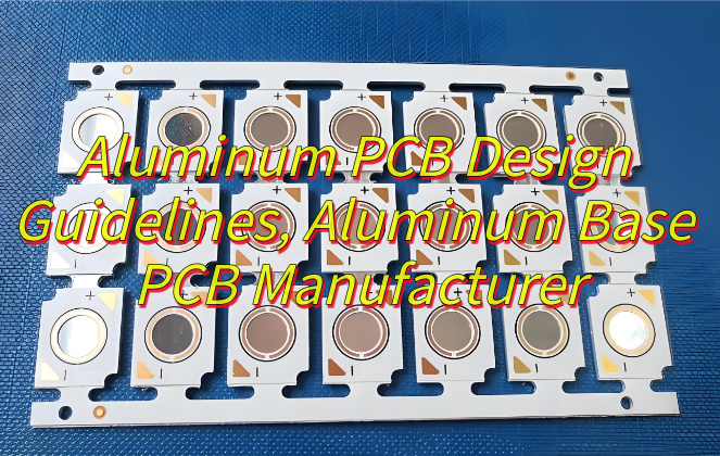
- Metal-core project support: review the aluminum-PCB construction together with LED pad geometry, dielectric choice, board-to-housing contact, outline tolerances, assembly temperature exposure, and requested material evidence.
- Prototype support: use sample builds to close placement, soldering, waveform, temperature, and optical-alignment questions. Record temporary materials or process differences so prototype evidence is not misapplied to production approval.
- Component sourcing and assembly: coordinate approved manufacturer part numbers, alternates, LED bin or wavelength requirements when specified, polarity controls, placement data, and incoming records within the released BOM.
- Production handoff: carry approved fabrication, assembly, inspection, and traceability requirements into mass production, with open deviations resolved before batch release.
- Quotation clarity: separate budgetary assumptions from fabrication-release and test-release inputs, allowing procurement to compare quotations on the same technical scope.
Send the available design package even if the project is still at the prototype stage. We can review which inputs are sufficient for quotation and which must be completed before manufacturing release.
FAQs About Driver Monitoring IR LED Aluminum PCBs
Q1: Should a DMS use 850 nm or 940 nm IR LEDs?
A1: 850 nm often provides stronger response from a silicon image sensor, but the emitter may show a faint red glow. At 940 nm, the illumination is less noticeable to occupants, while the selected sensor and optical filter may require a different current or exposure budget. Compare LED radiant output, sensor response, filter transmission, image quality, and the optical-safety assessment at the same wavelength before selecting the emitter.
Q2: When is an aluminum PCB preferable to FR4 for a DMS illuminator?
A2: Choose an aluminum PCB when the emitter board needs a short heat-spreading path into a metal housing and the circuit can be routed within the available metal-core construction. FR4 may suit a board that needs dense multilayer routing or combines more camera electronics, provided its thermal path meets the LED limits. Compare the complete junction-to-housing path and routing demand, not the substrate name alone.
Q3: Can the IR LEDs and LED driver be assembled on the same board?
A3: They can share one board when the driver can remain close to the LEDs without blocking the optical path or concentrating too much heat. A combined board shortens the pulse-current loop and removes an inter-board power connection, but it also places the switching node near the emitters and may restrict component placement. Use separate boards when optical packaging, heat separation, service access, or EMI isolation outweighs the shorter current path.
Q4: Can the illuminator PCB be separate from the camera PCB?
A4: Yes. A separate emitter board can be mounted where its beam and heat path work best while the camera PCB remains aligned with the lens. The added cable or connector must carry pulse current, trigger, and return signals without excessive voltage drop, ground shift, or timing error. Specify connector current capability, pinout, cable length, grounding, trigger thresholds, and shared mechanical datums across both boards.
Q5: How should IR LED polarity and orientation be documented?
A5: Put the same polarity and rotational orientation in the footprint, centroid file, assembly drawing, BOM notes, and inspection program. Mark the reference so it remains visible or traceable after panelization and component placement. Before production, compare one physical first article with the released drawing and functional test result. Conflicting polarity indicators must be resolved before placement programming, not corrected through operator judgment on the line.
Q6: Which optical datums belong in the PCB documentation?
A6: Identify the mounting features that locate the PCB in the housing, the LED optical centers, the camera optical axis, lens or diffuser references, and the critical board-to-camera offsets. Add position and rotation tolerances where they change illumination coverage. Dimension LED locations from the functional mounting datums; an accurate board edge does not protect alignment when that edge does not locate the module.
Q7: Should prototype validation include eyeglasses and sunglasses?
A7: Include representative eyewear when it belongs to the intended driver population. Lens coatings, curvature, tint, and frame position can create reflections or reduce the eye signal even when the uncovered face is evenly illuminated. Test the defined eyewear across the required head and seat positions under the same camera settings. Record the eyewear type and image acceptance result so later optical or LED changes can be compared with the same condition.
Q8: Can conformal coating be applied to an IR LED aluminum PCB?
A8: It may be possible when the coating material and process are compatible with the LEDs, solder joints, connectors, and operating environment. Define keep-outs around emitter lenses, optical surfaces, test points, connectors, mounting contacts, and the board-to-housing thermal interface. Confirm coating thickness, cure process, masking inspection, and rework method. Coating must not change the optical path or interrupt the intended metal-to-housing heat transfer.
Q9: Can AOI confirm that an IR LED works?
A9: AOI can check component presence, polarity or orientation features, placement, and visible solder conditions when the package and program provide adequate access. It cannot prove that the emitter produces the required radiant output, that the pulse current is correct, or that the camera receives uniform illumination. Add an electrical or optical functional test with defined drive conditions and acceptance limits for those requirements.
Q10: What should accompany first-article DMS illuminator samples?
A10: Agree on the evidence before the build. Depending on the purchase specification, the package may include fabrication and assembly revision identity, material and component lot records, dimensional or datum results, polarity and workmanship inspection, pulse measurements, thermal or optical results, approved deviations, and photographs of the accepted configuration. Link every report to the actual sample revision and serial or lot identity so the evidence cannot be confused with another build.
Conclusion
Before volume ordering, freeze the camera exposure, illumination geometry, pulse-current path, thermal interface, EMI controls, production data, and acceptance plan. Resolve any open item in the design review or quotation instead of leaving it for production interpretation.
If you are sourcing a driver monitoring IR LED aluminum PCB for an automotive DMS, send your Gerber/ODB++, BOM, quantity, stackup, assembly data, pulse profile, optical datums, thermal limits, and test requirements to sales@bestpcbs.com for engineering review and a quotation.