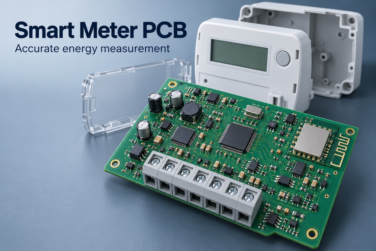
A smart meter PCB brings together the circuits that measure electricity consumption and transmit the readings. Inside a smart electricity meter, sensitive measurement signals share space with power supplies, processors, and communication hardware. Accurate readings depend on preserving those signals through PCB layout, assembly, and calibration.
EBest Circuit provides PCB fabrication and PCB assembly services for customer-approved designs, including mixed assemblies with SMT measurement circuits and through-hole power connections. Our team can coordinate board fabrication, component assembly, and agreed testing for prototype and production builds. Discuss your smart meter PCB project with us at sales@bestpcbs.com.
What Does a Smart Meter PCB Do?
A smart meter PCB connects the measurement circuit to the processing, storage, and communication electronics. Once assembled with components, it supports a clear signal path.
Voltage and current sensing → signal conversion → energy calculation → storage and communication
Voltage and current sensors produce signals that the analog front end and analog-to-digital converter can process. A metering IC or processor uses the samples to calculate power and accumulated energy. Memory retains readings, while communication hardware transfers data to other equipment or a utility network.
Power supplies, protection circuits, clocks, and display interfaces support this path. The communication interface enables remote data exchange; a digital display alone does not make a meter smart.
These functions can share one PCB or occupy separate metrology and communication boards. Separate boards allow communication options to change without replacing the entire metrology board, although their connectors and power interfaces still need to work together.
How Do Current Sensors Affect Metering Accuracy?
Current sensors influence both the amplitude and timing of the signal entering the metering circuit. An accurate ADC cannot recover information already distorted by sensor heating, phase shift, or saturation.
| Current Sensor | How It Measures Current | Sources of Measurement Error |
|---|---|---|
| Shunt resistor | Measures the voltage across a known resistance | Resistance tolerance, self-heating, temperature drift, and connection resistance |
| Current transformer (CT) | Converts alternating primary current into a secondary signal | Ratio error, phase shift, burden, and core saturation |
| Rogowski coil | Produces a signal proportional to the rate of current change, which is then integrated | Coil characteristics, positioning, and integration accuracy |
For a shunt, V = IR describes the sensing voltage, while P = I²R describes the heat generated. A higher resistance gives a larger signal at the same current, but also produces more heat. That temperature change can affect the resistance and the resulting measurement.
Phase error changes the relationship between the measured voltage and current signals, affecting active power calculation. Calibration can correct characterized gain and phase errors. It cannot reconstruct a clipped waveform or make a saturated sensor behave linearly.
How Does Smart Energy Meter PCB Design Keep Measurement Signals Stable?
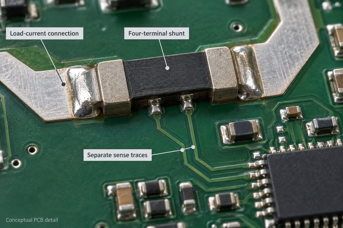
The layout must preserve the intended sensing voltage while keeping switching and communication currents out of its measurement path. Three connections deserve particular attention.
- Take shunt measurements from the intended sense terminals. Kelvin connections separate the voltage-sensing traces from the load-current connections. If the sense traces pick up additional voltage drop along a current-carrying connection, the ADC measures more than the shunt voltage.
- Keep filtering and decoupling close to the circuits they serve. Input filters must match the metering IC and sampling requirements because they affect amplitude and phase. Short local decoupling connections help keep supply disturbances from reaching sensitive circuitry.
- Give return currents a suitable path. Digital clocks, switching regulators, and transmitters should not force their return currents through sensitive measurement connections. Automatically splitting analog and digital ground can create detours; grounding should follow the device’s layout guidance while preserving required isolation barriers.
Communication activity provides a useful prototype test. If readings change when a transmitter becomes active, its supply demand or coupled noise may be reaching the measurement circuit. Comparing idle and transmitting conditions helps expose behavior that remains hidden during a quiet bench test.
How Are Mains and Communication Circuits Isolated?
Isolation separates circuits that must operate at different electrical potentials. In one common arrangement, the metrology circuit operates at a mains-related potential, while an external communication interface sits across an isolation barrier.
The barrier must account for both data and power.
- Data crosses through an isolation component, such as a digital isolator or an appropriate optocoupler, instead of a direct conductive signal connection.
- The circuitry on the isolated side needs a suitable power source. A shared ground connection through its supply can defeat the intended isolation even when the data signal passes through an isolator.
The PCB must maintain the barrier around copper, component pads, connectors, and mounting features. Creepage is the distance along an insulating surface; clearance is the distance through air. Their required values depend on the insulation requirements and operating conditions, rather than one universal spacing for every smart meter.
Low logic voltage does not guarantee a safe voltage relative to earth. Similarly, a CT can isolate the current-sensing connection while other parts of the measurement circuit remain connected to mains. Programming cables, shields, and test fixtures must also preserve the intended separation.
How Do PLC and Wireless Modules Change the PCB Layout?
PLC requires a controlled connection to the power line; wireless communication requires a suitable antenna environment. This difference changes where components sit and which areas of the PCB need protection from interference.
| Layout Feature | Power-Line Communication (PLC) | Wireless Communication |
|---|---|---|
| Signal connection | Coupling network connects the communication circuit to the power wiring | RF feed connects the radio to an integrated or external antenna |
| Space allocation | Line interface, coupling components, filtering, and protection | Module footprint, antenna area, and specified keepout |
| Sources of interference | Line noise and interaction with the switching power supply | Nearby switching circuits, unwanted coupling, and an unsuitable antenna environment |
| Product integration | Line connection and coupling network affect communication performance | Housing, terminals, shields, and nearby metal affect antenna performance |
For wireless modules, antenna keepout and ground-plane requirements are different parts of the layout. An antenna may require a clear area while the rest of the module needs a ground plane. The module’s instructions determine where each applies.
Both communication methods can place changing loads on the power supply. Supply capacity and local decoupling must accommodate transmission without disturbing metrology. Testing the assembled meter in its intended enclosure also captures effects that are absent when a bare board operates on the bench.
What Determines the Layers and Copper Weight of an Energy Meter PCB?
Layer count follows the routing and reference-plane requirements. Copper weight follows the current carried by the PCB conductors, their permitted voltage drop, and temperature rise.
Layer count depends on how the circuits fit and connect.
A simpler meter may fit on two layers. Additional communication interfaces, dense routing, and limited board space may make four or more layers useful. Extra layers can provide routing space and reference planes, but they do not automatically improve accuracy: sensing paths, return currents, and isolation still need the correct arrangement.
Copper weight depends on the actual load-current path.
The meter’s rated current is not necessarily the current flowing through its PCB traces. A shunt, busbar, or terminal structure may carry the main load while the board carries only sensing signals and electronics supply currents. In another design, substantial load current may pass through PCB copper.
This distinction comes before specifying thicker copper. Where the board does carry significant current, conductor geometry and copper thickness affect resistance and heating. Thick copper also draws heat away from solder joints, so its electrical benefit must be accommodated by the assembly process.
How Does Smart Meter PCB Assembly Handle Precision and Power Components?
Assembly must preserve the electrical characteristics of the measurement parts while forming sound connections to larger power components. The two areas need different process controls.
Metering resistors and ICs need the specified parts and connections.
Two resistors can have the same nominal resistance but different tolerances and temperature coefficients. Substituting one for the other in a sensing network can change readings as temperature changes, even though the meter starts normally. Part-number control therefore matters alongside placement and solder-joint quality.
SMT assembly handles the metering IC, processor, and small passive components. Placement and soldering must preserve the intended connections, especially around fine-pitch pins and closely spaced sensing components.
Power terminals and large copper connections need sufficient soldering heat.
Large terminals and copper areas absorb heat differently from small SMT joints. Too little heat can leave poor wetting or insufficient solder fill; an unsuitable thermal process can damage nearby components. The soldering profile and method must suit the complete assembly.
Through-hole parts may use selective, wave, or controlled manual soldering. Assembly order must leave access to those joints and to inspection areas. Visual or optical inspection identifies assembly defects, while electrical and metering tests determine whether the completed circuit operates correctly.
How Are Smart Meter Boards Programmed, Calibrated, and Tested?
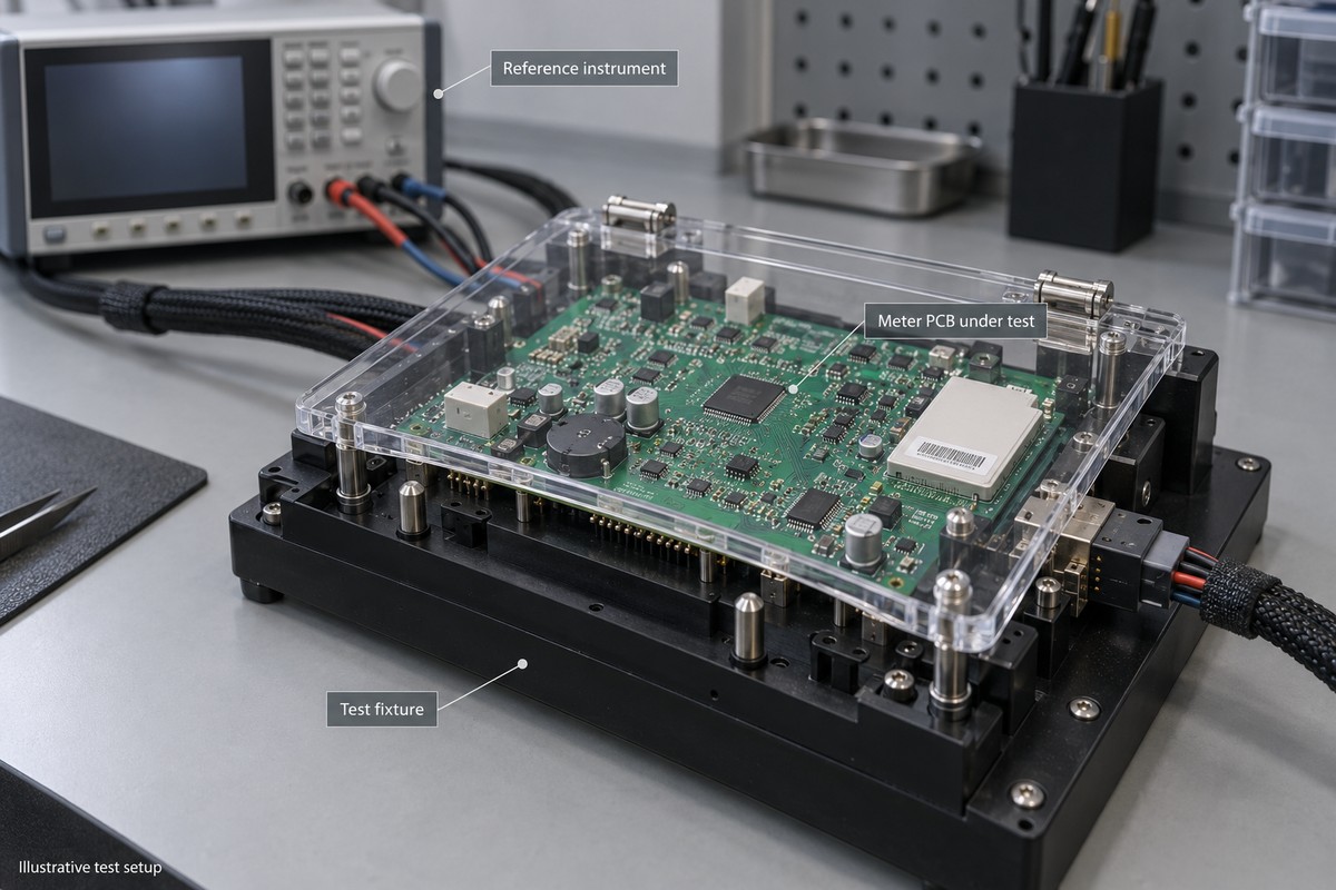
An assembled smart meter board is programmed with its intended firmware, calibrated against a reference, and then tested against defined acceptance limits. Calibration adjusts measurement behavior; verification measures the error that remains afterward.
- Load and verify the firmware and configuration. Programming installs the software and settings for the meter variant. Verification checks that the intended version and configuration were written successfully. Device identity is assigned where the product requires it.
- Compare the meter’s readings with a reference. The calibration setup applies known test conditions and compares the meter output with the reference result. Gain and phase corrections are calculated as required by the metering architecture; some designs also require offset correction. The resulting coefficients are stored for use during measurement.
- Measure performance after correction. Verification checks the remaining error at the current, voltage, and power-factor points defined for the product. Passing at the calibration point alone does not demonstrate accuracy across the operating range.
- Exercise the board’s other functions. Functional tests cover the power rails, display, memory, and supported communication interfaces. Power cycling checks whether required settings and calibration data are retained. Communication activity can also be included while measurement performance is observed.
The production record can associate each board’s identity with its firmware, calibration data, and test results. This makes a change in measurement performance easier to investigate across builds.
Production tests address the agreed board acceptance criteria. Complete meter certification also involves the applicable safety, EMC, environmental, and legal-metrology evaluations.
A reliable smart meter PCB build preserves the sensing connections, isolation boundaries, and component characteristics throughout manufacturing. EBest Circuit can support fabrication and assembly to your approved design, with testing agreed around the board’s actual functions. Contact sales@bestpcbs.com to discuss your prototype or production build.