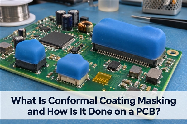
Conformal coating masking temporarily protects parts of a PCB assembly that must remain free of coating. The useful starting point is a no-coat drawing: identify the connector contacts, test interfaces, adjustable parts and other specified keep-outs, then select a mask that survives the chosen coating process and can be removed without damaging the board. A clean coating film is not a pass if it has entered a mating contact or a required test point.
For a coated assembly, masking belongs in the build instructions before coating starts, not in a last-minute operator guess. At EBest Circuit (Best Technology), our PCB assembly service covers board assembly, incoming component checks, inspection, cleaning and drying. When a project calls for coating, we review its material specification and keep-out drawing with the assembly files so the required work can be defined before quotation.
What Is Conformal Coating Masking?
It is the temporary protection of selected assembly features while a thin protective coating is applied elsewhere. Tape can define an edge, a reusable boot can cover a connector body, and a peelable liquid can bridge an irregular opening. The mask is removed at the stage specified for that coating-and-mask combination.
Do not confuse a temporary coating mask with the permanent solder mask on the PCB. The latter is part of board fabrication; it does not seal a connector’s mating face or identify every assembled component that must remain uncoated. Likewise, selective coating can reduce overspray, but it does not automatically eliminate every masking requirement near an open interface.
Which Parts of a PCBA Must Remain Uncoated?
Protect every feature for which coating would obstruct an electrical, mechanical or service function. Typical candidates include mating contacts, test pads that must be probed after coating, connector cavities, switch actuation surfaces and optical windows. These are candidates, not a universal prohibition: the assembly drawing and component instructions decide the actual keep-outs.
For example, an edge connector may need its contact fingers and insertion zone kept clear, while a nearby solder joint can be coated. Masking the whole connector region is easy to draw but may leave too much exposed circuit. Masking only the visible gold fingers may miss a cavity into which liquid coating can wick. The boundary must be drawn around the functional interface, not merely the component outline.
| Feature | Define on drawing | Check after de-masking |
|---|---|---|
| Mating connector | Contact face, cavity opening and allowable boundary | No film or mask fragment in the mating path |
| Post-coat test point | Probeable pad and access clearance | Probe makes the specified electrical contact |
| Adjustment or switch | Moving interface and surrounding keep-out | Motion and electrical operation remain as specified |
| Optical window | Clear aperture and edge condition | Required optical path remains clear |
How Should No-Coat Areas Be Marked on the Assembly Drawing?
Show a no-coat boundary on a revision-controlled assembly view, name the affected reference designators and state whether the boundary applies to the top, bottom or both sides. A component note such as “mask J3” is incomplete if it does not identify whether the entire housing, only the mating cavity or also the surrounding PCB must be kept clear.
Use the same orientation and datum as the assembly drawing. If a dimension matters, locate it from a board feature or component datum and specify its tolerance in the project drawing. A coating supplier cannot derive a safe mask margin from a photograph or a highlighted rectangle alone.
- Mark each no-coat feature on the correct board side and revision.
- Identify the functional surface and the permissible coating edge.
- State the coating material and application method, because flow and overspray change the boundary risk.
- Record how the first article will be inspected before the map is released to production.
Where a connector has both a solderable tail and a mating cavity, annotate those surfaces separately. The coating may be intended around the tail but prohibited inside the cavity; a single component-wide keep-out loses that distinction.
How Do You Mask Connectors and Mating Contacts?
Choose a barrier that seals the particular entry path without pressing on delicate contacts. A fitted boot can enclose a connector face; tape can cover a flat opening or edge; a dispensed peelable mask can follow a shape that tape will not seal. The mask must remain seated during application and release cleanly at removal.

Before coating, inspect the mask from the direction in which liquid can enter. A boot that looks secure from above can leave an unprotected side gap; a strip of tape can bridge a recessed cavity without actually sealing it. Check both the contact face and the perimeter where the coating will arrive.
If an edge finger or bare-copper area is involved, material compatibility matters. Techspray’s current WonderMASK PX product sheet specifically warns against using that latex grade on bare copper because discoloration may occur. That is a restriction on the named product, not proof that all peelable masks have the same behavior.
What Must Be Checked Before Masking Begins?
Start with a clean, dry assembly and a matching set of drawing, BOM and coating instructions. Oil, flux and moisture can undermine coating adhesion and can also make a temporary tape seal unreliable. The MG Chemicals coating application guide specifically places substrate cleaning and drying before masking and coating for its products.
Then confirm three identities: the board revision, the coating material and the mask material. A mask qualified with one solvent system or one curing route should not be silently carried into another. Inspect sample edges, seams and cavities before committing a production lot.
- Board: correct assembly revision, connector orientation and no-coat drawing.
- Materials: coating grade, selected tape/boot/liquid mask and their compatibility instructions.
- Route: application method, cure sequence and planned removal point.
- Evidence: first-article photographs or inspection records for the actual keep-out features.
How Does the Coating Method Change the Masking Plan?
Dip coating surrounds the assembly and makes an open connector cavity a direct exposure path; manual spray can drive material past a loose tape edge; selective coating reduces the coated area but still needs a defined boundary at tight interfaces. Brush work may avoid broad overspray yet can leave a local bead or run. The masking method should be chosen against the actual route, not against the product name alone.
MG Chemicals lists brush, spray, dip and selective application for its conformal-coating products. Its guide notes that brush application can be useful for small work or repair but may not achieve the same consistency as spray. Select the actual route and material before fixing the mask geometry; the same connector can need different protection under spray and dip conditions.
Consider a board with an open board-to-wire connector beside a tall component. Under a spray route, review spray direction and the connector’s side opening, then examine the boundary after the first coated board. Under a dip route, protect the whole cavity before immersion. The same top-view keep-out line does not prove both routes are controlled.
When Should Masking Be Removed?
Remove the mask when the selected coating and maskant instructions say the edge can be released without pulling coating from the protected area or leaving residue. There is no universal “always before cure” or “always after cure” answer. A dry-to-touch coating, a partially cured solvent coating and a fully UV-cured film behave differently at the mask boundary.
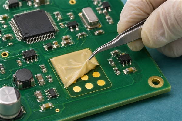
Dymax’s electronic masking bulletin recommends removing certain maskants before curing UV conformal coatings, allows a partial-cure window for some solvent-based coatings and describes removal after parylene deposition for suitable materials. That sequence is product-specific; the actual coating, maskant and process sheet must be matched before release.
For the first article, record the coating state at removal and inspect the edge immediately afterward. If a strip lifts adjacent coating, the response is to revisit the removal window and edge geometry, not simply pull harder on subsequent boards.
How Do You Inspect the Boundary After De-Masking?
Inspect both sides of the intended line: the protected interface should be free of coating, while the adjacent required-coated area should not have been lifted or left with a gap. Look into connector cavities, around mask edges and at any test feature used after coating. A top-view photograph alone may miss residue inside a recess.
Where the coating has a UV tracer, UV inspection can help locate the film, but the tracer and inspection lighting must suit the actual coating. Functional checks answer a different question: a connector mating check or a specified probe test may reveal an obstructed interface that a visual check missed. Neither one replaces the other.
Record a nonconformance against the specific no-coat drawing feature: reference designator, board side, observed encroachment or lifted edge, affected quantity and disposition. That record is more useful than a generic “masking failed” note because it tells the team which boundary and which process step need correction.
What Causes Coating Leakage and Mask Residue?
Leakage usually points to a real entry path: a raised tape edge, a boot that does not fit, a gap at a connector wall, or coating flow that exceeds the first-article setup. Residue has different causes, including unsuitable adhesive chemistry, insufficiently cured peelable material or removal outside its qualified window. Do not treat the two defects as one repair problem.
Use a defect-to-action record rather than adding more tape blindly. If coating entered J3’s cavity from one side, photograph the route, check the boot fit or tape seal in that direction, then repeat the same application route on a first article. If adhesive is left on a test pad, check the mask material and removal method before approving cleaning; the pad’s surface finish may constrain what can be used.
The adjacent coating also needs review after rework. Removing unwanted film from a contact can disturb the required film beside it; the board should be rechecked against both sides of the no-coat boundary before release.
How Should a First Article Validate the Masking Plan?
Run one approved assembly through the actual cleaning, masking, coating, curing and de-masking sequence, then inspect the designated keep-outs before repeating the route. A paper drawing can show intent, but only a process-matched first article shows whether the tape edge or boot fit holds under the selected application direction.
For example, designate connector J3 as the critical feature. Record the intended no-coat boundary on the drawing, the selected mask, the coating method and the removal point. After processing, photograph the contact face and side entry path, check for film or residue, and perform the agreed mating or electrical check. If a side gap lets coating enter, change the mask fit and repeat the same check; changing the drawing note alone has not fixed the process.
Keep the first-article record linked to the material and drawing revisions. The result establishes that this particular combination was observed to work; it is not a blanket qualification for another connector, coating chemistry or board geometry.
What Should You Send for a Coated PCBA Quote?
Send us the assembly drawing, BOM, coating specification and an explicit no-coat map with the PCB files. State the target application method if it is fixed, the required coating thickness and inspection criteria if they are defined by the project, and which functional interfaces must remain accessible after coating. We use these inputs to define the masking work that the quotation must cover.
For an EBest Circuit assembly inquiry, include build quantity, component supply arrangement and any first-article evidence or customer approval step. We can review the PCB assembly inputs with your coating requirements and identify the masking, inspection and documentation work that the quotation needs to cover.
What Are the Detailed Parameters of a Peelable Mask?
A peelable mask is not specified by the word “liquid” alone. Application thickness, viscosity, drying or cure time, substrate compatibility and removal method affect whether it can cover the required keep-out without running into a contact. The following values apply to Techspray WonderMASK PX product 2222, according to its Rev. C (09/26) technical data sheet.
| Parameter | Published value for product 2222 | Selection consequence |
|---|---|---|
| Application thickness | 15-20 mil (0.381-0.508 mm) recommended for use | Check whether the dispensed bead fits the no-coat feature |
| Viscosity | 9,000-16,000 cP | Use the named product’s dispensing guidance |
| Ambient cure time | 15 min typical | Check actual thickness and humidity before coating |
| Removal | Peelable | Confirm access to grip and remove the full mask |
| Bare copper | Not recommended by manufacturer | Select a compatible alternative for bare-copper contact areas |
For a 0.30 mm-wide test pad that must remain exposed, the published 15-20 mil application thickness does not tell us how far a dispensed mask will spread sideways. Check the actual dispense footprint against the pad and adjacent coating boundary on a first article. If the material covers the pad or cannot be peeled away cleanly, change the mask geometry or use a more controllable barrier.
The same data sheet warns against bare-copper use and states that drying time varies with thickness and humidity. Use the current supplier revision for the selected material rather than copying these values to a different grade. See the manufacturer’s Rev. C data sheet for the underlying values.
Masking Tape vs Boots vs Peelable Mask: Which Fits?
Use tape for a reachable flat boundary, a fitted boot for a repeated three-dimensional connector opening, and a peelable mask for a local shape that the other two cannot seal cleanly. This is a starting choice, not a ranking of quality: each option can fail through an unsealed edge, material incompatibility or difficult removal.
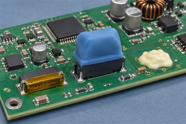
| Decision point | Tape | Boot | Peelable mask |
|---|---|---|---|
| Best-fit geometry | Flat edge or accessible planar area | Repeatable connector body/opening | Irregular local shape or opening |
| Critical setup check | Adhesive and edge seal | Fit and side-entry gaps | Dispense footprint and cure |
| Removal check | No adhesive residue or lifted coating | No contact damage or trapped coating | Complete peel with no fragments |
| Re-use | Normally single use | Possible if product and cleaning route permit | Single use |
For J3 in the first-article example, a boot is attractive if it seals the side opening repeatedly; tape may be better if only a flat contact face needs protection. A peelable material is plausible where the profile is irregular, but its bead must not enter the contacts and must remain removable. Compare the first-article boundary and labor for the actual board, not just the purchase price of a masking consumable.
Conformal Coating Masking FAQs
Can selective coating eliminate masking?
Sometimes it reduces the number of masks, but it does not automatically protect an open connector or a tight no-coat edge. Check the real deposition path and first-article boundary.
Is solder mask the same as conformal coating?
No. Permanent PCB solder mask is made during board fabrication; conformal coating is applied to the assembled board. Temporary coating masking protects selected assembled features during that later operation.
Can masking tape be left on after coating?
Not by default. Temporary masking should be removed at the approved point in the coating process, and the protected feature checked for residue and coating intrusion.
How do you tell whether masking worked?
Compare the processed board with the no-coat drawing: the functional interface is clear, the adjacent required-coated area remains covered, and any specified mating or electrical check passes. Preserve the first-article record for that material and revision.
For your conformal coating masking plan, send the no-coat drawing and coating specification with the PCB assembly files to sales@bestpcbs.com. We can review the assembly inputs and define the project-specific coating scope before quoting.