A laminated busbar lowers inductance when the outgoing and return currents follow closely spaced, overlapping copper plates. It helps less if the current must separate at the capacitor terminals, mounting tabs or switching module. Before choosing a laminated busbar over a heavy copper PCB, trace the complete switching current loop and compare the inductance of the assembled paths, not just the copper weight or the busbar by itself.
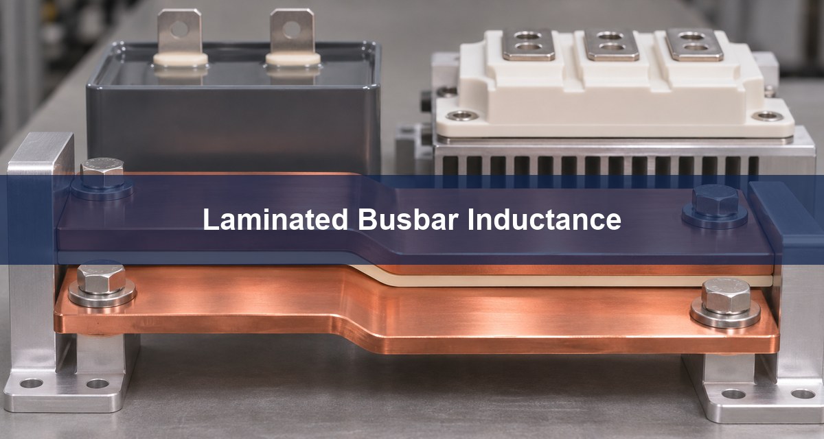
Laminated busbar inductance
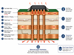
Inductance describes the voltage associated with changing current. In a laminated pair, close parallel plates carrying equal currents in opposite directions confine much of the magnetic field between them. The loop usually has less inductance than two conductors routed far apart. Thick copper lowers DC resistance, but it does not by itself bring the return path closer. In a heavy copper PCB, closely spaced power and return planes can use the same principle.
Keep two numbers separate: the inductance between the busbar’s defined terminals and the effective inductance of the assembled switching loop. A low first number does not guarantee a low second one. Infineon’s PrimePACK application note shows how a laminated DC-link connection is arranged at a module.
DC link busbar
The DC-link busbar connects the DC source and capacitor network to the switches. The path carrying average supply current need not be the path carrying the fastest current change. For a half-bridge, trace the loop from the effective local DC-link capacitor through the switch positions and back to the opposite capacitor terminal. Include the capacitor’s terminal and internal inductance, the busbar or board conductors, the joints and the module package. Clearly identify which external paths are outside this loop.
For example, an inverter layout may have a long DC feed and a short, well-coupled path to the nearest film capacitor. Shortening the feed does not necessarily fix switching overshoot. Conversely, moving a capacitor closer by straight-line distance may not help if its terminal geometry forces the positive and negative connections apart.
Commutation loop inductance
As a first-pass estimate, the inductive voltage contribution is L × |di/dt|. If the design allocates 40 V to this contribution and the applicable current slope is 4 A/ns, the effective loop budget is 10 nH. This is an illustrative allocation, not a device limit. An estimated 15 nH at the same slope contributes approximately 60 V. Do not add that number directly to a measured peak as if ringing, device capacitance and observation point did not matter.
The useful quantity belongs to a defined loop under the conditions of interest. Changes in current distribution and mutual coupling can make a schematic sum of isolated conductor values misleading. The published study on SiC converter busbar design separates the busbar, capacitor, connector and package contributions and shows why the terminals belong in the analysis.
DC link capacitor busbar
Review both capacitor terminals with the return route visible. A large remote capacitor bank can support stored energy and slower ripple while a nearby low-inductance path supplies fast switching current. Parallel capacitors do not automatically share high-frequency current equally: different placement, terminations and parasitic inductances change the current distribution. A short broad path is only helpful if it remains paired with its return close to the capacitor and at the module.
In the inverter example, if the positive tab is on the near edge and the negative tab returns around a mechanical opening, the loop can be dominated by that opening rather than by the flat overlap. Ask for the assembled geometry and compare alternative terminal orientations before paying for a thicker pair of plates.
Laminated busbar design guide
Choose a laminated assembly when separate formed conductors better meet current, mechanical or terminal constraints. Choose a heavy copper PCB when closely paired layers meet the same loop budget and integration is more important. Use separate conductors only when the fast switching loop is controlled elsewhere or when measured inductance still meets the requirement.
| Construction | When it fits | What to verify |
|---|---|---|
| Laminated busbar | Broad paired conductors are possible, with heavy terminal loads. | Plate overlap at the tabs, assembly alignment and the insulation system. |
| Heavy copper PCB | A layered return path and integrated routing fit on one board. | Layer spacing, via and terminal transitions, current distribution and temperature rise. |
| Separate bars | The conductors carry feed current and a separate compact path closes the fast loop. | The location of the actual switching loop and measured switching stress. |
A busbar’s dielectric spacing cannot be chosen from inductance alone. For products where IEC 60664-1 applies, coordinate the insulation design with the responsible compliance engineer and the applicable product standard. Close spacing does not waive separate checks at exposed edges, cutouts and terminals.
Busbar inductance calculator
Use a parallel-plate estimate only to compare the straight, broad overlap regions with the same assumptions. In its wide-plate limit the estimate is μ₀ times overlap length times plate separation divided by width, for a nonmagnetic spacer. For a 100 mm long overlap, 50 mm wide, with 0.50 mm separation, this gives about 1.26 nH. Doubling separation gives about 2.51 nH with the other inputs unchanged. These are idealized straight-section estimates, not assembled loop values or measured data.
The estimate assumes closely spaced plates, approximately opposing currents and width much greater than separation. It omits end effects, joints, apertures and curved tabs, and does not predict current crowding or resonant impedance. Use field extraction or a supplier model with the actual geometry and frequency band if a transition can dominate. Record the port pair on every result so that two nominally identical values are comparable.
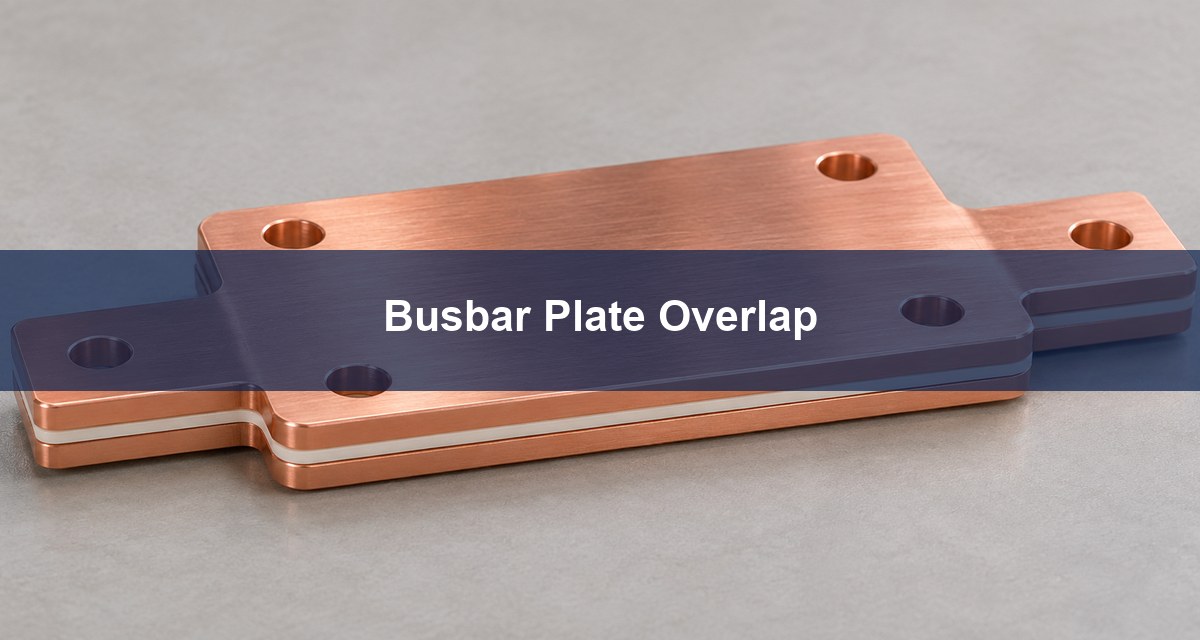
Laminated busbar manufacturing process
Manufacturing must reproduce the conductor spacing and alignment used in the electrical review. Do not approve a busbar from a front-view drawing alone. Specify the plate stack, terminal datums, allowed misalignment and the insulating construction at holes, edges and bends. A nominal spacing that looks favorable in a field model is not enough if the assembled tabs must splay apart to reach the module.
For the related heavy copper board, define the board stackup and joint geometry that form the same current path. The Best Technology busbar PCB design article covers broader board integration. The product drawing and contract should identify the applicable board performance requirements, for example IPC-6012 for qualifying a rigid board where specified; that does not qualify the separate busbar insulation or the assembled loop.
Double pulse test waveforms
On a qualified laboratory setup, compare turn-off voltage and current at the same reference points under comparable DC-link voltage, current, device temperature and gate-drive conditions. An apparent improvement can come from a slower current edge, a different measurement loop or probe error. Log the current slope, peak voltage, ringing and exact setup with each trace. A bench switching waveform by itself does not certify insulation, thermal performance or behavior over all operating points.
| Evidence | What it answers | What to hold constant or record |
|---|---|---|
| Simplified overlap estimate | How the straight section responds to geometry changes. | Plate length, width and separation; model omissions. |
| Field extraction or impedance measurement | Whether termination and connection geometry dominate the path. | Port locations, fixture treatment and frequency range. |
| Switching waveforms | Whether peak stress meets the design budget on a representative assembly. | Switch, gate drive, DC-link voltage, current, temperature and probe reference. |
Release the change only after representative switching conditions meet the project’s documented voltage margin. If the model improves but the waveform does not, revisit the capacitor path, the terminal transition and measurement setup before another copper revision.
FAQ
Does thicker copper automatically lower the switching-loop inductance?
No. It can lower resistance, but the proximity and continuity of the opposing current paths drive much of the geometric inductance.
Why can the nearest capacitor still behave as if it is far away?
Its effective path includes both terminals and the complete return. A short positive lead with a long negative return can still produce a large loop.
Can a busbar have low DC resistance and high switching overshoot?
Yes. Voltage drop in steady operation and inductive voltage during fast current change are different measurements.
Is a low supplier inductance number enough to release the assembly?
No. Ask where it was measured and whether it includes the joints, module and capacitor path used in the final assembly.
Can I fix poor geometry by adding more bulk capacitance?
Not necessarily. If the extra capacitor is coupled through the same high-inductance path, it may affect slower ripple more than the switching edge.
Does a tighter laminated stack always help?
It can reduce the straight-section inductance, but an insulation or assembly constraint may set the minimum spacing. The tabs can still dominate.
Is busbar inductance the same as gate-loop inductance?
No. The gate-drive loop is a separate path with its own reference and geometry. Improving the power path does not automatically correct gate ringing.
What belongs in a fabrication review package?
Send the assembly drawing with terminals, board stack, current-loop sketch, any insulation constraints and the switching conditions used for your limit.
Prepare a heavy copper PCB review
Contact Best Technology at sales@bestpcbs.com with your stackup, terminal drawing and current-loop sketch. Identify whether you need a board-based current path or an external busbar interface so the mechanical and board constraints can be reviewed together.