To move from breadboard to PCB, first record the circuit that actually works, then capture its schematic, assign purchasable parts and footprints, lay out the board, and validate the fabrication files against the electrical design. A photograph of jumper wires can help you remember the prototype, but it is not a netlist or a manufacturing file. At EBest Circuit (Best Technology), we can review the resulting PCB package and assemble a prototype when the board, BOM and assembly information agree.
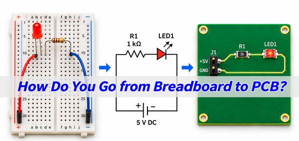
What Does Breadboard to PCB Mean?
A solderless breadboard connects components through spring contacts hidden under rows of holes. A PCB replaces those temporary contacts and jumpers with specified copper traces, pads, plated holes and soldered parts. Converting the project is therefore a design transfer, not a direct print of the breadboard’s physical layout.
The new board also needs decisions the breadboard did not force: connector orientation, mounting holes, component availability, trace clearances, ground return, test access and assembly method. A simple LED prototype may transfer with few changes. A radio, motor driver or precision analog circuit may need substantial redesign because jumper length and contact behavior concealed important electrical effects.
When Is a Breadboard Circuit Ready for a PCB?
Freeze the prototype only after its intended functions work at the required supply range and load. Record the actual component values, device part numbers, pin assignments, polarity and the measured behavior you expect the board to reproduce. A circuit that lights an LED once is not necessarily ready if it must also start reliably, survive a changed supply or fit an enclosure.
Keep a dated photograph and a connection list, then remove one jumper at a time if its destination is unclear. Check the hidden breadboard rail split and row numbering rather than trusting colored wires. If you changed a resistor or moved a connection during debugging, the final record must reflect that working state, not an earlier drawing.
Can I Use a Breadboard Instead of a PCB?
Yes, while you are testing and changing a circuit on the bench. A solderless breadboard lets you move parts and probe connections without ordering a new board. If it provides stable contact for the components and conditions you are testing, there is no need to make a PCB just to answer an early design question. Record the working connections and measurements before changing the layout again.
A breadboard is not a drop-in substitute when the build must be mounted in an enclosure, handled or moved in service, or reproduced with the same wiring and component positions. Spring contacts and jumper wires can loosen or be connected differently from one build to the next; their long, uncontrolled paths can also affect circuits sensitive to noise, timing or high-frequency behavior. At that point, transfer the verified circuit into a schematic and design a PCB for the actual electrical, mechanical and assembly requirements.
Breadboard vs Perfboard vs Custom PCB: Which Should You Choose?
Choose by the next task, not just by whether the circuit works. A breadboard is fast for reversible experiments. Perfboard or a solderable breadboard can make a one-off circuit permanent while leaving most point-to-point wiring manual. A custom PCB makes the interconnect, placement, outline and assembly data repeatable.
| Question | Solderless breadboard | Perfboard / solderable prototype | Custom PCB |
|---|---|---|---|
| Will the wiring change again? | Best for frequent changes | Rework requires soldering | Changes require a design revision |
| Is the same build needed repeatedly? | Jumper placement varies | Manual wiring must be documented | Controlled artwork and BOM support repeats |
| Must it fit an enclosure? | Limited mechanical control | Possible with manual layout | Outline, holes and connectors can be defined |
| Is automated assembly intended? | No | Usually not economical | Possible with assembly-ready data and suitable parts |
If the circuit changes daily, another breadboard iteration is usually cheaper than revising ordered boards. A custom PCB starts to make sense when fit, repeatability or assembly time matters more than the freedom to move a jumper. Budget for fabrication, components and, if needed, assembly and a test fixture; bare-board and assembled-prototype costs cover different work.
How Do You Record the Breadboard Connections?
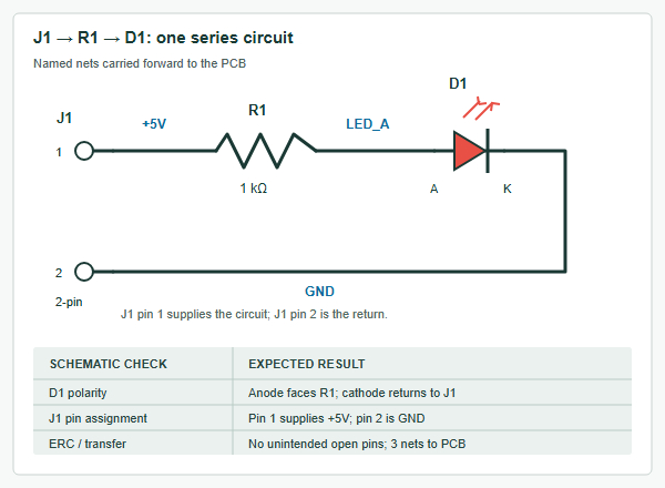
Follow one 5 V indicator circuit through the conversion: J1 pin 1 feeds a 1 kΩ resistor R1; R1 feeds the anode of red LED D1; D1’s cathode returns to J1 pin 2. Record the three nodes below while the breadboard still works. Each row names both endpoints, so the same information can be checked in the schematic and later in PCB copper rather than inferred from wire colors.
| Node | Connections on the working breadboard | Connection to preserve on the PCB |
|---|---|---|
| +5V | J1 pin 1 to R1 pin 1 | J1 pad 1 to R1 pad 1 |
| LED_A | R1 pin 2 to D1 anode | R1 pad 2 to D1 anode pad |
| GND | D1 cathode to J1 pin 2 | D1 cathode pad to J1 pad 2 |
Confirm the three nodes with the power off and a continuity meter, particularly if the breadboard rail is split. Keep a photo to locate physical parts, but use the node table as the electrical input to the schematic. For a larger design, record every connector pin and module interface the same way; a wire color or breadboard row number alone does not define a net.
How Do You Rebuild the Schematic?
Create the three symbols in a schematic editor: a two-pin power connector, a 1 kΩ resistor and an LED with its anode toward the resistor. Give the connections the same +5V, LED_A and GND names as the node table. The result below shows the electrical circuit rather than the physical breadboard rows; a breadboard to circuit diagram converter can help with capture, but it cannot determine hidden breadboard contacts from a photograph.
In KiCad, assign reference designators and values, save the schematic, then run Electrical Rules Check (ERC). An unconnected pin means the captured circuit is incomplete; an unpowered-net warning may need a power-source declaration if the design really receives power through J1. Resolve the electrical intent before selecting footprints. KiCad’s 9.0 tutorial shows the schematic-to-board workflow used in the next step.
What Changes When a Breakout Board Becomes a Component?
A plug-in module may contain parts the breadboard experiment hides: a voltage regulator, pull-ups, level shifting, filtering or a USB interface. Replacing that module with a bare chip does not preserve those functions automatically. Read the module schematic and the chip manufacturer’s design requirements before deciding what remains on the custom board.
For an Arduino breadboard to PCB project, decide whether the first PCB will hold the complete controller module on headers or reproduce its circuitry. The module-on-headers option usually reduces first-build risk but uses more space; a chip-level redesign can be smaller but needs its own power, programming and reset plan. Label the chosen boundary on the schematic and BOM.
Read the exact breakout’s schematic rather than assuming that every module contains the same support circuit. Trace each external pin back to its function and note the module’s supply range, logic level and required connections. If a regulator or level shifter was on the old board, either keep that board in the assembly or add an equivalent function to the new schematic; the bare IC alone will not replace it.
How Do You Select Parts and Footprints?
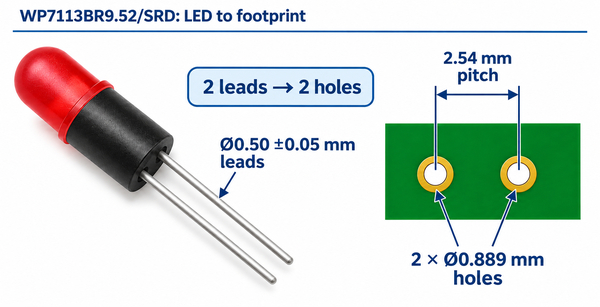
Choose footprints from the parts that will actually be purchased, not from the breadboard hole pattern. For D1, the Kingbright WP7113BR9.52/SRD drawing gives two Ø0.50 ±0.05 mm leads on 2.54 mm centers and a two-hole Ø0.889 mm recommendation. The corresponding footprint needs two pads at that pitch, the correct anode/cathode mapping and room for the LED body. The figure compares that part with its two-hole pattern.
Apply the same drawing-to-footprint check to the selected resistor and connector: lead span, body clearance, pin numbering and cable approach may differ even if their schematic symbols are unchanged. Once a part number is chosen, keep its BOM entry, footprint and assembly orientation together. A 1:1 print or a physical fit trial can expose a mechanical mismatch before ordering the board.
How Do You Place and Route the PCB?
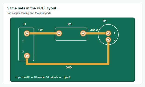
With footprints assigned, use Tools → Update PCB from Schematic (F8 in KiCad 9). The PCB editor should import the three footprints and show unconnected lines for +5V, LED_A and GND. Draw the outline, place the connector at an accessible edge and orient the LED so its polarity remains visible after assembly. The layout diagram below shows how the same three nets can be routed after placement.
Route each net to the pads already assigned by the schematic, then run Design Rules Check (DRC). A clean ratsnest only proves that the intended nets have been connected in the editor; inspect the copper, clearances, outline and mounting features as well. The breadboard’s left-to-right order has no authority over placement. We can fabricate the two-layer board from approved files after reviewing its drill, clearance and outline details.
Leave probe access for the supply, LED_A and ground so first-board measurements are practical. More complex transfers also need fresh layout decisions that a breadboard never settled: place supply decoupling near the IC it serves, size current paths for the actual load, and check return paths and connector access. Those requirements come from the circuit and component data, not from the 3 mA LED example.
What Detailed Parameters Should Be Fixed Before Fabrication?
Fix the dimensions and manufacturing requirements that the prototype actually needs. For this small indicator board, 50 × 30 mm is a starting outline, not a standard size; the chosen connector and enclosure decide the final edge and hole locations. Two-layer, 1.6 mm FR-4 is a practical starting construction where no thickness-critical interface is specified. None of those choices follows automatically from using a breadboard.
| Drawing field | Choice for this example | Why this value / next check |
|---|---|---|
| Board outline | 50 × 30 mm starting envelope | Fit J1, R1, D1 and three probe points; finalize against actual placement and enclosure |
| Layers / material / thickness | 2-layer FR-4, 1.6 mm nominal | Simple routing and available stock choice; verify connector and enclosure fit |
| Outer copper | 1 oz starting foil | The 3 mA LED branch does not demand heavy copper; check final stack-up |
| Trace / gap | 0.25 / 0.25 mm minimum in this layout | Leaves more routing margin than our listed normal 0.10 / 0.10 mm capability; not a universal 5 V rule |
| D1 plated lead holes | 2 × Ø0.90 mm finished, 2.54 mm pitch | Based on Kingbright’s 2 × Ø0.889 mm recommended layout and Ø0.50 ±0.05 mm leads; verify finished-hole tolerance |
| Optional plated signal via | Ø0.30 mm finished | Only if a net changes layers; never use this value for D1’s leads |
| Mounting holes | Only if the enclosure calls for them | Take diameter and centers from the actual mechanical design |
One fit calculation makes the hole choice traceable. The LED’s largest specified lead is 0.55 mm; a Ø0.90 mm finished plated hole with our published FR-4 PTH tolerance of ±0.075 mm has a minimum opening of 0.825 mm. The resulting 0.275 mm diametral clearance is an initial fit check, before lead forming, hole position and the actual sample are considered. A Ø0.30 mm optional via is for a layer transition, not for this LED lead; finished-hole size is not the same as the drill-tool diameter.
The 0.25/0.25 mm trace and gap in the table leave routing margin above our listed normal 0.10/0.10 mm capability; they are not a universal rule for 5 V circuits. Current, voltage spacing, pad rings and thermal demands must be evaluated from the real design. If the project has high current, sensitive signals or a tight enclosure, those requirements may drive a different copper weight, layer stack or outline than this indicator example.
What Should You Check Before Ordering?
Run ERC on the schematic and DRC on the PCB, then open the plotted Gerbers and drill files in an independent viewer. The viewer should show the intended copper, solder mask, silkscreen, outline and finished-hole locations. A successful editor check does not prove that an old or wrong export was sent to the factory; compare the export date and revision with the board you approved.
Make one final physical check using the actual connector and enclosure: pin 1, cable entry, LED visibility, tool access and hole centers must fit the assembly. If a part was substituted after layout, confirm its land pattern and polarity before release. This mechanical pass answers questions that ERC cannot see and is more useful than repeating the schematic connection list.
Which Files Should You Send for PCB Fabrication and Assembly?
For a bare PCB, send the copper, solder-mask and legend Gerbers, drill data, outline and fabrication drawing from the approved board revision. In KiCad, plot the fabrication layers and generate the drill files from that same saved board, then inspect the output rather than assuming the current editor view is the delivered package. Assembly adds the exact BOM, placement data and orientation drawing.
| Deliverable | PCB fabrication | Assembly / test | Cross-check before release |
|---|---|---|---|
| Gerbers + drill | Required manufacturing geometry | Board reference | Same revision, units, origin and outline |
| BOM | Usually not needed for bare boards | Part sourcing and substitutions | Exact MPN, value, package and designator |
| Placement data | Not a bare-board substitute | Part positions and rotation | Coordinate origin and pin-1 convention |
| Assembly drawing | Mechanical context as needed | Side, orientation and special instructions | Matches BOM and placement data |
| Test instruction | Electrical bare-board test if specified | Prototype function and acceptance record | Supply, loads, measurements and limits |
Our PCB assembly service can manufacture the board and assemble selected parts when their identities and placement instructions are complete. For this example, the BOM names the LED model and the actual resistor and connector ordered; the assembly drawing gives LED polarity and connector orientation. For a larger design, include programming and functional-test instructions if those services are requested. The four files in the table serve different production tasks and cannot substitute for one another.
How Do You Test the First PCB Prototype?
Begin with a power-off inspection of polarity, solder joints and supply-to-ground resistance. Apply a current-limited supply and measure the voltage at the board connector. In the example series branch, if the board measures 5.0 V and the LED measures 2.0 V, a verified 1 kΩ resistor should drop 3.0 V. That implies 3 mA and about 9 mW in R1. The 2.0 V LED drop is an assumed measurement for this example, not a guaranteed value for the chosen part at 3 mA.
If D1 is dark, first confirm the probe points, reference and polarity of each voltage reading, then measure directly across R1. A steady 3.0 V drop across a verified 1 kΩ resistor means about 3 mA is flowing through R1. In the intended single path, a completely open LED or reversed, nonconducting LED cannot coexist with that reading. Check whether the PCB follows the schematic, whether an unintended bypass carries the resistor current, or whether the LED conducts without visible light; do not diagnose an open connection from the voltage numbers alone.
If R1 has little or no drop while 5.0 V remains at the board connector, an open path, reversed LED or bad joint becomes plausible; locate the missing voltage along the series path. If the board rail collapses, investigate supply limiting or a short before drawing a conclusion about D1. Record the supply setting, measured rail, component drops and observed light so the first build has a result that can be repeated after a repair or design revision.
What Common Breadboard-to-PCB Mistakes Cause Rework?
The most costly mistakes are often missing information rather than a poorly drawn trace: an undocumented change to the working prototype, a breakout function omitted from the new schematic, or a connector that fits the PCB but cannot accept its cable inside the housing. Each error enters at a different stage, so repeating ERC alone will not catch them all.
Keep the original node record, the selected part drawings and the approved board revision together. When a first board fails, compare what was built against those three sources before editing the circuit. If the board matches the files but the function is still wrong, revisit the electrical design; if it does not match, correct the specific fabrication or assembly discrepancy and test again.
How Can We Support the First Build?
We fabricate FR-4 prototypes and can combine board production with PCB assembly. We accept prototype assembly orders without a fixed MOQ and review supplied files for manufacturability. For a first build, we can flag drill, outline or assembly-data questions before production, while the approved electrical design remains the basis for the board we build.
For a breadboard to PCB prototype, send the released Gerbers or PCB files, schematic, BOM, assembly drawing, target quantity and any board-level test requirements to sales@bestpcbs.com. Tell us whether you need bare boards or assembled prototypes. We can clarify missing fabrication or placement details, define the requested assembly and test scope, and prepare a quotation for the agreed build.
Breadboard to PCB FAQs
Can software turn a breadboard photo directly into a PCB?
No photo can reliably supply every hidden contact, component identity, rating and manufacturing constraint. Breadboard to PCB software can help capture a schematic and route a board once the connections and parts have been verified, but the design transfer still needs human checks.
Can I send only Gerbers to order an assembled prototype?
Gerbers can describe board artwork, but assembly also needs the exact BOM, component placement and orientation information, plus any programming or functional-test instructions. A bare-board order and an assembled-board order therefore require different packages.