Finding a BGA void does not automatically mean the solder joint will fail, and it does not automatically justify rework. The decision depends on how much of the joint is affected, where the void sits, whether the pattern repeats, and which acceptance requirement governs the build.
A single percentage cannot answer all four questions. The useful path is to read the full X-ray pattern, separate measurement from acceptance, and then connect the result to paste deposition, reflow, moisture exposure, or PCB pad and via design. That turns an image into a decision instead of a reason to change several process variables at once.

What Is a BGA Void?
A BGA void is an unfilled cavity trapped inside a BGA solder joint after reflow. It can originate in the package solder ball, the printed solder paste, or the combined joint formed when the ball and paste coalesce during BGA soldering. Because the package hides the array, internal voids are normally assessed with X-ray inspection.
A void is not the same as a bridge, missing ball, nonwet open, or head-in-pillow condition. Those defects form differently and may require other views or tests. Confirm the defect type before calculating a void percentage or changing the assembly process. Record the indication first; make the acceptance decision only after its context is known.
What Causes BGA Voids to Form?
BGA voids form when gas, flux volatiles, or trapped air cannot escape before molten solder solidifies. The sources fall into four practical groups:
- Material-related causes: paste chemistry, flux activity, moisture, oxidation, or contamination can add gas or interfere with wetting.
- Printing-related causes: the shape and consistency of the paste deposit influence trapped air, solder volume, and the route available for gas to leave.
- Reflow-related causes: the thermal profile determines when volatiles are released, how well the solder wets, and how long gas can escape before solidification.
- PCB pad and via-related causes: land geometry, via-in-pad construction, and local copper distribution alter solder flow, heat transfer, and solder wicking.
Several groups can act together. The X-ray pattern narrows the search; paste records, SPI, thermal data, and PCB information identify the actual cause.
Are BGA Voids Always a Reliability Problem?
No. A BGA void is an internal cavity, not an automatic declaration that the solder joint is defective. Some joints with voiding remain serviceable, while others deserve attention because of their geometry and the product’s operating conditions.
An X-ray indication should therefore trigger an engineering evaluation rather than immediate rework. Removing a BGA adds another thermal cycle and can introduce pad, package, or alignment damage, so the rework decision should follow the applicable acceptance requirement and the actual risk to the assembly.
The lower-risk response is to document the indication, review the governing requirement, and compare the complete array before deciding whether further testing or rework is justified.
Which BGA Voids Are More Likely to Affect Reliability?
Voids are more likely to affect reliability when they remove a large part of the joint, sit near a critical interface, form a cluster, or recur at stressed ball locations. The same void geometry deserves more attention in assemblies exposed to strong mechanical or thermal loads.
Pay closer attention when:
- Large area loss: a single void occupies a large part of the joint.
- Critical location: the void is close to an interface or likely crack path.
- Clustered geometry: several nearby voids reduce the effective solder area in one region.
- Repeatable coordinates: the same ball locations show voiding across multiple boards.
- High service load: the assembly faces vibration, bending, drop, or repeated thermal cycling.
Do not decide from total percentage alone. Compare the largest void, its location, the distribution across the array, and the product’s expected loads. A higher-risk pattern calls for closer verification, not an automatic conclusion.
How Are BGA Voids Detected and Measured?
BGA voids are normally detected by X-ray inspection for PCB assembly, where they appear as lighter regions inside the darker solder-joint projection. The first task is to confirm that the indication is inside a joint and then read it in the context of the complete array.
- Size: compare the largest individual void and the total affected area rather than counting bright spots alone.
- Location: note whether the void is central, near an interface, or aligned with a via or other PCB feature.
- Pattern: distinguish one isolated indication from clusters, rows, corners, or a region that shares the same thermal or design influence.
- Repeatability: compare the same ball coordinates across more than one board to separate a random event from a fixed process or PCB factor.
Inspect the whole array before enlarging one joint. Use a consistent exposure and orientation, record the ball coordinate, and retain the original image. That makes later comparisons traceable and reduces the chance that one unusual joint is mistaken for a package-wide trend.
Projected void area ratio = total projected void area inside the joint ÷ projected solder-joint area × 100%
For example, 0.050 mm2 of visible voiding inside a 0.503 mm2 projected joint area gives about 9.9%. The result can change with image angle, magnification, contrast, and the selected boundary, so comparisons need the same setup and method.
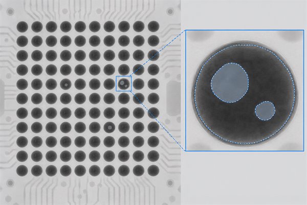
The measurement is not an automatic pass or fail. X-ray describes projected geometry; acceptance still depends on the governing requirement, the void’s position and distribution, and the product risk.
What BGA Void Percentage Is Acceptable?
There is no single BGA void percentage that can serve as a universal pass/fail limit. Acceptance follows the document and revision specified for the project, together with the measurement method and the joint condition shown by the X-ray.
A practical decision follows this order:
- Identify the governing requirement. The customer specification, drawing, contract, or applicable IPC document establishes the acceptance basis for that build.
- Confirm the measurement method. The reported ratio should be traceable to a defined X-ray view, threshold, and projected joint boundary.
- Review the largest individual void. This distinguishes one dominant cavity from the same total area spread across smaller voids.
- Consider location and distribution. Interface-adjacent, clustered, or repeated voids may justify further review even when the total percentage is unchanged.
- Compare the array and production lot. A stable isolated result and a worsening repeated pattern should not receive the same process response.
Figures such as 10%, 20%, or 25% are not universal BGA acceptance limits. A value quoted online may come from another document revision, product class, package type, or measurement convention. Use a numerical limit only when the project requirement makes it applicable. If the build documents do not specify one, settle the acceptance basis and review authority before production rather than inventing a threshold after inspection.
How Do Solder Paste and Stencil Printing Affect BGA Voids?
Solder paste controls volatile release and wetting, while stencil printing determines the volume and shape of each deposit. Paste that is beyond its storage, conditioning, or floor-life limits can behave differently; moisture exposure or contamination can add gas or disrupt wetting. Printing variation can then change both solder volume and the escape path.
Irregular results from ball to ball often justify checking SPI volume, alignment, aperture release, stencil cleanliness, and paste handling before changing the oven. A consistent footprint-wide pattern points more strongly toward paste chemistry, aperture design, or a stable print setup. Confirm the correction when SPI stability and the next X-ray pattern improve together.
How Does the Reflow Profile Affect BGA Voiding?
The reflow profile affects BGA voiding by controlling when volatiles are released, when solder coalesces, and how long gas can escape. Aggressive heating can trap gas after coalescence begins; insufficient time above liquidus can limit wetting; excessive heat can exhaust the flux or increase oxidation and warpage risk.
Widespread voiding may reflect a profile that does not suit the paste and board mass, while one row or corner may expose a temperature difference across the package. Measure the real ramp, soak, time above liquidus, peak, and temperature spread with thermocouples at representative locations. Adjust within material and component limits, then compare the next build using the same X-ray method.
How Do PCB Pad and Via Designs Contribute to BGA Voids?
PCB pad and via designs contribute to BGA voiding when they change solder volume, wetting, heat flow, or the path into which molten solder can wick. Open or incompletely filled via-in-pad structures can pull solder away from the joint and leave an indication aligned with the via.
Voids that recur at the same coordinates, follow via locations, or concentrate near different copper mass point toward a fixed board feature. Compare the X-ray with the land pattern and fabrication data, then verify via fill, cap, planarity, and pad dimensions on the delivered PCB. The actual construction, not the drawing alone, shows whether solder wicking or thermal imbalance is present. Check both design intent and delivered-board evidence before changing the assembly process.
How Can You Find the Root Cause of BGA Voids?
The fastest route to a likely BGA void cause is to match the X-ray pattern with the process or design evidence that could produce it. The image supplies a direction; SPI, thermal data, material history, and PCB information confirm or reject it.
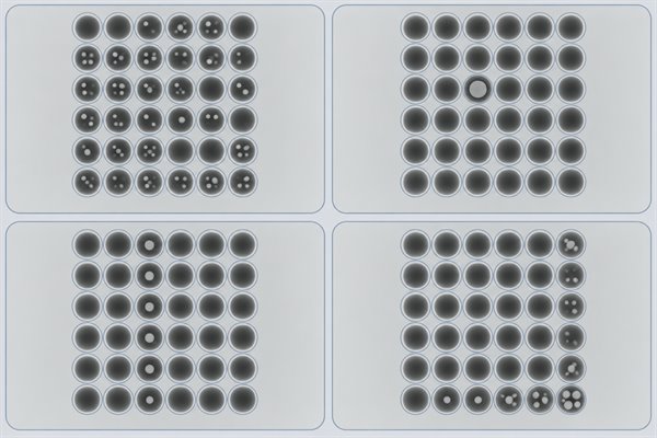
| X-Ray Pattern | Likely Cause Area | Check First |
| Many small voids | Paste or reflow behavior | Paste condition, SPI stability, and the measured thermal profile |
| One large isolated void | Local printing or wetting | SPI at that pad, pad surface condition, and contamination evidence |
| Voids aligned with vias | Via-in-pad construction | Via fill, cap, planarity, and evidence of solder wicking |
| One row or corner affected | Thermal imbalance or warpage | Temperature distribution across the BGA and board flatness |
| Same coordinates on many boards | Fixed design or process factor | Pad, via, copper, tooling, and repeatable process patterns |
A pattern is a starting hypothesis, not a final diagnosis. Start with the broadest repeatable feature, because an array-wide change is usually more informative than the most visually dramatic joint. Then work through five practical moves:
- Check whether it repeats. Compare several boards and the same ball coordinates.
- Match the pattern to evidence. Review SPI, the measured profile, material history, and PCB features.
- Choose the strongest explanation. Predict which joints should change if that explanation is correct.
- Change one leading variable. Keep the other major conditions stable so the trial is readable.
- Recheck the same locations. Improvement supports the cause; no change means the next explanation should be tested.
How Can You Reduce and Prevent BGA Voids?
Prevent recurring BGA voids by holding proven material, printing, thermal, moisture, and PCB conditions stable and confirming that the improvement repeats.
- Stabilize paste and printing. Keep paste within its handling limits, maintain the stencil, and use SPI to confirm consistent volume and alignment.
- Profile the actual assembly. Use thermocouple data from the real board and BGA rather than copying an oven recipe from another product.
- Control moisture and contamination. Follow the documented storage, floor-life, handling, cleaning, and any required baking limits.
- Verify pad and via construction. Confirm that delivered boards match the corrected via fill, cap, planarity, and land geometry.
- Use a repeat-build check. Inspect the same coordinates with the same X-ray setup on the next build and confirm that the improvement holds across the agreed sample.
One improved image is not enough. Treat the correction as proven only when the process evidence and X-ray result repeat. Higher-risk products may also need electrical, mechanical, or qualification testing because X-ray alone cannot predict field life.
FAQs About BGA Voids
Q1: Can a BGA pass functional testing and still have a hidden solder-joint problem?
A1: Yes. Functional testing confirms operation under the applied conditions, not the internal shape of every joint. A marginal connection may behave differently during bending, vibration, or thermal cycling, so test results and X-ray evidence answer different questions.
Q2: Should a BGA be reworked solely because voids appear on an X-ray?
A2: No. Rework adds thermal and handling risk. First confirm the defect type, applicable acceptance requirement, void location, and repeatability. An ambiguous image may need another view before the package is removed.
Q3: What information should a useful BGA X-ray report include?
A3: The report should make the decision reproducible. Include the assembly identity, BGA part number, lot, array orientation, ball coordinates, overview and detail images, measurement method, governing requirement, and disposition. Preserve the original images for later comparisons.
Q4: Can 2D X-ray reliably distinguish a void from head-in-pillow?
A4: Not in every case. A 2D image is a projection, so overlapping materials can hide an interface separation. Another X-ray view or physical analysis may be needed when the image and electrical symptom do not agree.
Q5: What should be checked after BGA rework?
A5: Review the complete reworked array. Check alignment, ball shape and collapse, bridges, opens, voiding, and regional differences. Compare with the earlier image when available, then complete the appropriate electrical or functional test.
Q6: When is destructive analysis justified for a suspected BGA void problem?
A6: It is justified when nondestructive evidence cannot resolve an important failure question. Cross-sectioning or dye-and-pry can confirm interface cracking, pad separation, intermetallic condition, or true void geometry when a sample can be sacrificed. Preserve the X-ray, electrical results, and build history first.
Conclusion
A BGA void should lead to an evidence-based decision, not automatic rework. Confirm the defect type, compare its size, location, distribution, and repeatability, measure it with a consistent X-ray method, and apply the requirement that governs the build. If the pattern repeats, change one likely cause at a time and treat the correction as proven only when the next build shows repeatable improvement.
Unsure whether a BGA void calls for rework or a process adjustment? Email sales@bestpcbs.com with the X-ray image and BGA part number. If available, include the Gerber or ODB++ files and the applicable acceptance requirement. EBest Circuit can review the pattern and help you determine what to verify before rework or the next build.