Choose a dogbone fanout if the offset via, short connecting trace and remaining escape channels fit the approved fabrication rules. Choose a qualified via-in-pad structure when the offset land blocks the escape, not merely because the BGA pitch looks small. A simple diagonal clearance check shows why an apparently workable 0.5 mm grid can fail before any trace is routed.
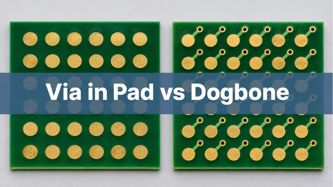
Via in Pad vs Dogbone
A dogbone places the via beside the BGA pad and connects them with a short trace. A via-in-pad places the hole within the solder land. Moving the via can recover space on the top layer, but it can also change the assembly, stackup and inspection requirements.
| Option | Choose it when | Main constraint |
| Offset dogbone | Via and routes clear adjacent pads | Needs room between balls |
| Filled and capped via in pad | Offset via blocks escape and capped process is qualified | Land flatness and fabrication steps |
| Blind microvia in pad | Approved stackup reaches the needed layer | Target landing and via reliability |
Start with the exact package drawing. The worked geometry below is hypothetical and must not replace the component vendor’s layout recommendation.
BGA Pitch 0.5 Mm
Pitch measures center-to-center distance, not the free channel between solder lands. For the example, pitch is 0.50 mm, BGA copper land diameter is 0.28 mm and the chosen offset via land diameter is 0.30 mm. Assume a 0.09 mm copper spacing requirement and a 0.09 mm escape trace, before checking package-specific mask, registration and process rules.
| Input | Teaching value |
| Ball grid pitch | 0.50 mm |
| BGA copper land | 0.28 mm diameter |
| Offset via land | 0.30 mm diameter |
| Trace and spacing | 0.09 mm each |
Those dimensions are geometry inputs, not recommendations. Use the manufacturer’s actual land pattern and the fabricator’s approved design limits.
Dogbone Fanout BGA
For a via centered in the square between four balls, the center distance to each surrounding land is pitch ÷ √2. At 0.50 mm pitch, that distance is about 0.354 mm. Subtract the 0.140 mm solder-land radius and the 0.150 mm via-land radius. The resulting nominal copper gap to a different-net neighbor is about 0.064 mm.
That is below the hypothetical 0.09 mm clearance. The same-net connection to the chosen pad is allowed, but the adjacent nets still need clearance. If you move the via toward one pad, recheck all other neighbors and the neck trace rather than assuming the shift fixes the entire cell.
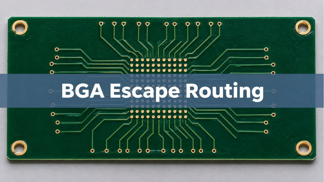
BGA Escape Routing
Check the straight escape channel independently. Two 0.28 mm lands on a 0.50 mm row leave 0.22 mm between their edges. One 0.09 mm trace plus two 0.09 mm gaps needs 0.27 mm, so this route also fails on that layer. Moving the offset via into the pad does not make that between-land channel wider.
Decide where signals actually leave the footprint. A blind via can move a net to a different layer, but that layer has its own plane openings, land sizes and routing congestion. Evaluate representative corner and interior pins in the same model before assigning a via technology to the whole package.
Via in Pad Filled and Capped
If the solderable land contains a through via, specify the agreed fill, cap and surface condition, not just “via in pad.” The finished surface should meet the assembly requirements for the particular footprint. An open or merely tented hole is not equivalent to a qualified filled and plated-over land.
Check the Best Technology VIPPO process guide for construction and inspection details. On the drawing, identify which pad groups need the process and the evidence that will show the finished structure is correct.
Via in Pad Solder Wicking
Open vias in a solder land can draw solder away during reflow. A feature that passes copper clearance can therefore still fail assembly. Ask the assembler to review the land, solder mask, paste and via treatment together. Check whether the available inspection method can detect the relevant joint or via issue.
If only the inner balls need via-in-pad, keep the simpler offset fanout on the outer rows if it passes the checks. Document the two structures separately so the shop does not assume they share the same treatment.
PCB Via Aspect Ratio Calculator
Aspect ratio depends on drilled depth and the diameter definition used by the process owner. For example, a 1.00 mm through depth and a 0.20 mm drilled diameter give 5:1 under that simple convention. Do not use the finished hole in that calculation if the qualified process specifies drilled diameter.
Use the actual layer-to-layer depth and approved diameter for a blind microvia. A through-hole ratio does not predict blind-via landing, dielectric clearance or stacked-via reliability. Confirm the proposed structure with the fabricator before treating it as a viable escape option.
BGA Fanout Guidelines
Release the fanout when the selected package lands, copper and mask rules, via structure and complete layer escape all pass. Verify at least one representative crowded cell, including nonconnected neighbors, and inspect the first article using the evidence specified for the chosen structure.
In the example, the offset via and straight channel both fail. First test a supplier-approved smaller offset geometry or a different routing approach. If neither works, qualify a via-in-pad stackup, verify the receiving layers, and rerun assembly and signal checks before release.
Frequently Asked Questions
Is via in pad required for every 0.5 mm BGA?
No. Pitch alone does not determine the fanout. Land diameters, trace spacing, ball assignment, approved via geometry and stackup all matter. Try the package manufacturer’s recommended land pattern and run the two clearance checks before deciding whether a higher-density fabrication process is necessary.
Can I simply make the BGA pad smaller to fit the dogbone?
Do not shrink a solder land solely to make routing easier. First check the exact package’s recommended footprint, the assembler’s process and the mask design. Changing the pad changes the solder-joint geometry. Consider a different layer escape or qualified via structure if the recommended land does not fit.
Is the via land diameter the same as the drill diameter?
No. The via land is the copper area around the hole. Its outer diameter controls spacing to adjacent copper. The hole diameter and its definition matter for fabrication and aspect ratio. Use the actual land dimensions for the geometric check and the approved drill data for process review.
Can I put dogbones on the outer rows and via in pad inside?
Yes, when each structure fits its own geometry, assembly and electrical constraints. Check that the outer rows still leave escape channels for the signals that need them. Identify which vias are filled and capped so the fabrication drawing and the released drill data remain unambiguous.
Does solder mask prevent solder wicking into a pad via?
A solder mask cover alone is not a substitute for a specified solderable filled and capped surface. Mask registration and opening geometry matter. Use the approved via construction for the assembly and ask the assembler how it will check joints when the via sits inside the solder land.
Will a blind microvia always eliminate an extra routing layer?
No. It changes where a signal can leave the pad. The receiving layer must still have room for the via lands, traces and reference structure. Test a real net assignment and routing pattern before changing the layer count or estimating the savings from an HDI process.
How should I handle a clearance result close to the limit?
Keep the full precision of the geometry and compare it with the fabrication design rules, including the agreed tolerances. Rounding a marginal gap up is not a design fix. Ask for a manufacturing review of a representative cell and include its pad, mask and drill data.
What should I send for a BGA fanout review?
Provide the exact package and land-pattern drawing, routed footprint, net assignments, layer stack, via definitions, and trace and spacing requirements. Identify which pins are difficult to escape and which via-in-pad areas need inspection. This makes it possible to compare real options instead of guessing from the pitch.
References
- AMD UG1099: BGA Ball Pad, Via and Trace Dimensions
- Altera AN 766: Dog-Bone Topology
- TI: nFBGA Packaging
Discuss Your PCB Requirements
For a Best Technology fabrication review, send the BGA land pattern, proposed via structures and a representative fanout cell to sales@bestpcbs.com. Include the layer stack and the clearance that fails.