EBest Circuit is an automotive HDI PCB supplier in China that supports custom HDI PCB fabrication, laser microvia processing, SMT assembly, and inspection for ADAS controllers, automotive cameras, infotainment systems, and vehicle communication modules.
Automotive buyers need more than a small advertised feature size. The supplier must connect the released stackup, microvia geometry, material lot, assembly plan, inspection records, and change controls to the same order so that prototype approval can transfer into repeat production.

What Automotive Applications Require HDI PCBs?
HDI becomes useful when fine-pitch packages, dense signal routing, or limited board area make a conventional through-hole fanout impractical. Microvias connect selected adjacent layers while preserving routing channels for high-pin-count devices.
- ADAS camera modules: Image processors, memory, and high-speed interfaces can require dense BGA escape routing within a compact enclosure.
- Domain and autonomous-driving controllers: High-pin-count processors and memory buses may need multiple controlled-impedance layers and short signal paths.
- Infotainment systems: Processor, display, storage, and communication circuits often compete for limited board area.
- Automotive Ethernet gateways: Dense communication circuitry needs controlled-impedance paths, continuous reference planes, and connector-aware routing.
- Battery monitoring modules: Compact sensing and control layouts can benefit from selective microvias when isolation and creepage requirements are also maintained.
HDI is not automatically the right choice for every vehicle circuit. High-current power distribution may still favor wider conductors, heavier copper, or a separate power board rather than additional microvia build-up layers.
What Specifications Should You Send for an Automotive HDI PCB Quote?
A useful quotation needs the complete construction, not isolated minimum feature sizes. Send the stackup, layer connections, copper weights, impedance table, material requirements, surface finish, panel constraints, and the tests that must appear in the acceptance package.
| RFQ field | Initial capability reference | What must be approved |
| Layer count and build-up | 2 to 16 layer HDI; 1+N+1, 2+N+2, and higher-order structures subject to review | Released stackup, lamination sequence, dielectric thicknesses, and via connections |
| Laser microvia | 0.10 mm (4 mil) capability reference | Finished diameter, target pad, capture pad, dielectric depth, and filling requirement |
| Fine line and space | 0.075/0.075 mm (3/3 mil) special capability reference | Copper thickness, finished conductor tolerance, plating route, and inspection method |
| Microvia aspect ratio | 1:1 or lower is a common design target | Actual laminated dielectric thickness divided by finished microvia diameter |
| Materials | High-Tg FR-4, CAF-resistant, or specified low-loss laminate | Manufacturer, grade, Tg, Dk/Df where relevant, thickness, and substitution policy |
| Controlled impedance | Project-specific | Target, tolerance, layer, trace geometry, reference plane, coupon, and report format |
| Surface finish | ENIG, ENEPIG, OSP, or another approved finish | Finish thickness, solderability requirement, storage limit, and assembly compatibility |
Microvia diameter must be assessed with dielectric depth and pad geometry. A nominal 0.10 mm laser microvia through a 0.075 mm dielectric has an approximate depth-to-diameter ratio of 0.75:1, but the released value must come from the actual laminated stackup.
What Manufacturing Risks Need Extra Control?
Microvia interfaces, layer registration, warpage, insulation resistance, and via-in-pad planarity deserve separate controls. A final continuity test cannot reveal every latent interconnect or assembly risk.
- Microvia fatigue: Repeated thermal expansion can stress the microvia-to-target-pad interface. Geometry review, controlled drilling and plating, microsection evidence, and specified thermal testing address different parts of this risk.
- Layer misregistration: Each sequential lamination cycle can move features relative to earlier layers. Material compensation and in-process registration checks help keep the laser target within its released annular geometry.
- Board warpage: Asymmetric build-ups and unbalanced copper can deform the panel during fabrication or reflow. Copper balance, material symmetry, lamination control, and a defined flatness limit reduce this exposure.
- CAF exposure: Moisture, electrical bias, spacing, material selection, and drilling quality interact. CAF-resistant laminate alone does not replace spacing and process control.
- Via-in-pad solder loss: Incomplete filling, poor capping, or uneven planarization can draw solder away from a BGA joint. Filling and surface planarity should be verified before assembly.
Stacked microvias add interfaces through the build-up. Where the routing permits, staggered structures may reduce unnecessary stacked interfaces and simplify qualification.
How Are Automotive HDI PCBs Manufactured and Assembled?
The approved via map determines the number of lamination, laser drilling, metallization, and filling cycles. The fabricator should freeze that route before panel production because a stackup change can alter impedance, registration, reliability, cost, and schedule.
- DFM review: Check the stackup, via structure, copper thickness, materials, impedance table, panel drawing, and acceptance files before CAM release.
- Inner-layer fabrication: Form and inspect the inner circuits, including buried-via subassemblies where the design requires them.
- Sequential lamination: Add each build-up layer under controlled pressure, temperature, and registration conditions.
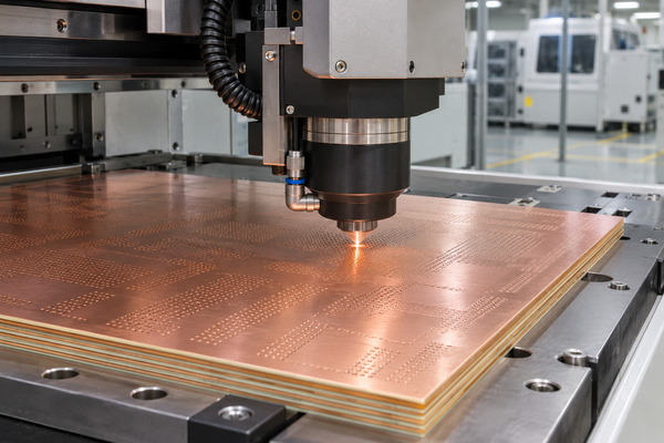
- Laser drilling and metallization: Drill the released microvias, prepare their surfaces, and deposit and plate copper. Repeat only for additional build-up levels.
- Via filling and outer-layer completion: Fill and cap specified vias, form the outer circuitry, and complete solder mask and surface finish.
- Bare-board inspection: Run electrical testing plus specified dimensional, microsection, impedance, and visual checks.
- SMT assembly: Apply solder paste, place components, reflow, inspect visible and hidden joints, and run the agreed electrical or functional tests.
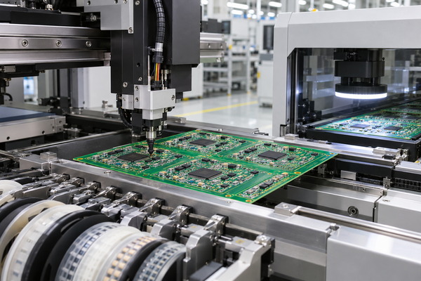
A bare board can pass continuity while still having pad flatness or via conditions that affect BGA soldering. The fabrication and assembly teams should therefore review via-in-pad requirements against the same released data.
How Are Automotive HDI PCBs Tested for Reliability?
The test plan should connect each method to a defined failure mode and acceptance criterion. AOI, electrical test, microsection, impedance measurement, thermal exposure, X-ray, and functional testing are complementary rather than interchangeable.

- AOI: Detect conductor pattern defects such as shorts, opens, and etching anomalies at the relevant production stage.
- Electrical test: Compare continuity and isolation against the released netlist.
- Microsection analysis: Examine selected microvia interfaces, plated-hole structures, copper thickness, and internal registration.
- Impedance measurement: Check released coupon structures against the specified target and tolerance.
- Thermal stress or cycling: Apply a defined temperature profile and acceptance rule to the interconnections selected for qualification.
- IST when specified: Track resistance change during repeated thermal loading for the defined coupon or structure.
- X-ray and functional test: Inspect hidden assembly joints and verify the assembled module against the agreed test specification.
Electrical test alone proves net continuity at that moment. It does not establish long-term microvia reliability, so the qualification plan must reflect the actual operating environment and customer requirements.
Which Certifications and Quality Documents Should a Supplier Provide?
Verify the manufacturing site, certificate scope, order-level records, and customer-specific approval package separately. A management-system certificate does not certify an individual PCB design or prove a particular process limit.
- Quality-management scope: IATF 16949 is an automotive quality-management-system standard aligned with ISO 9001. Ask for the current certificate, named site, scope, issuing body, and validity.
- Bare-board requirements: IPC-6012F covers rigid printed board qualification and performance, while the IPC-6012FA automotive addendum applies when the procurement documents require the matching automotive requirements.
- Material traceability: Request laminate and copper identification, lot records, certificates where required, and a Certificate of Conformance tied to the shipment.
- Inspection evidence: Define the electrical, impedance, microsection, dimensional, first-article, and assembly reports that must accompany the order.
- Production approval: Specify PFMEA, Control Plan, PPAP level, approved samples, and change-notification requirements when the customer program requires them.
The purchase order and released drawing should name the applicable standard revision and any customer-specific acceptance rules. General website statements cannot replace that order-level definition.
How Do You Evaluate an Automotive HDI PCB Supplier in China?
A qualified automotive HDI PCB supplier must show that its production route, quality controls, documentation, and delivery plan match the released design. Compare suppliers against the same RFQ package so that a lower quote is not based on a different stackup or inspection scope.
- Construction fit: Confirm the exact layer count, build-up, microvia type, copper weight, fine features, and materials rather than accepting a generic HDI label.
- Reliability evidence: Ask how drilling, plating, via filling, registration, microsection sampling, and any specified thermal tests are controlled for this construction.
- Site and QMS fit: Match the proposed manufacturing site to the certificate scope, process ownership, traceability route, and customer-specific requirements.
- Fabrication-to-assembly handoff: Confirm who owns via-in-pad planarity, stencil review, BGA inspection, rework limits, and functional-test fixtures.
- Revision control: Require one approved data package and written approval before material, site, stackup, finish, or process changes.
- Quote transparency: Compare the same quantity, panelization, tests, documentation, tooling, components, freight terms, and schedule assumptions.
- Repeat-production control: Check how approved materials, process parameters, inspection records, and golden-sample references are retained for reorder.
- International delivery: Define protective packaging, shipment split, destination, incoterm, shipping documents, and delivery milestone.
The best fit is the supplier that can reproduce the approved construction with checkable records, not the one advertising the smallest single feature.
Why Choose EBest Circuit as Your Automotive HDI PCB Supplier?
EBest Circuit can combine HDI fabrication, component sourcing, SMT assembly, inspection, and project documentation under one RFQ path. Final capability and documentation commitments remain tied to the released files and quotation.
- Custom HDI fabrication: Review approved multilayer build-ups with laser microvias, blind or buried vias, via filling, and fine-line circuitry.
- Free DFM check: Review the stackup, microvia geometry, copper dimensions, impedance inputs, panelization, and via-in-pad requirements before production release.
- Fabrication and assembly coordination: Align bare-board manufacturing, component sourcing, SMT, AOI, X-ray, and agreed functional testing through one project team.
- Traceable records: Define material, lot, electrical, impedance, inspection, and assembly evidence in the quotation rather than assuming a standard package.
- Prototype-to-production control: Carry the approved revision, construction, materials, and inspection plan from engineering samples into repeat orders.
Send the complete RFQ package so the engineering review can distinguish mandatory automotive requirements from optional tests or documentation.
Illustrative Automotive HDI RFQ: 8-Layer Three-Stage Construction
This is an illustrative quotation scenario, not a released customer case or proof of qualification for a specific vehicle program. It shows the inputs that must stay consistent when several HDI build-up cycles are required.
| Input | Illustrative value | Release check |
| Construction | 8-layer rigid board with three HDI build-up stages | Complete layer and via map for every build-up cycle |
| Material | FR-4, Tg 180 class | Exact manufacturer, grade, thickness, and substitution restriction |
| Finished thickness | 1.6 mm nominal | Finished tolerance and stackup calculation |
| Copper | 1 oz inner and outer layers | Base copper versus finished plated copper definition |
| Via treatment | Specified resin-filled vias | Via list, fill type, capping, planarization, and acceptance method |
| Surface finish | ENIG | Thickness requirement and compatibility with assembly and storage |
The manufacturing review should verify registration through each lamination cycle, microvia and filled-via interactions, panel movement, impedance geometry, and the inspection samples required for approval. Use in an automotive program would still require customer-specific qualification and reliability evidence.
What Affects Automotive HDI PCB Manufacturing Cost?
Build-up cycles, via processing, fine features, materials, inspection, documentation, and order quantity drive the quotation. The lowest-cost route is usually the simplest construction that still meets routing and reliability needs.
- Sequential lamination: Each build-up level adds imaging, lamination, laser drilling, metallization, inspection, and yield exposure.
- Microvia structure: Filled, stacked, skipped, or via-in-pad features add process and acceptance requirements.
- Fine-line combination: Finished copper thickness and conductor tolerance affect whether 3/3 mil features are practical for the chosen layers.
- Material control: High-Tg, CAF-resistant, and low-loss grades differ in price, availability, storage, and processing behavior.
- Automotive evidence: Extra coupons, thermal tests, first-article records, traceability, PPAP work, or customer-specific documentation add cost.
- Order and panel efficiency: Tooling, setup, test programming, panel utilization, attrition, and component procurement distribute differently across prototypes and volume orders.
Ask every bidder to price the same released construction and evidence package. Otherwise, a cheaper quotation may simply omit a lamination stage, specified material, test, or approval record.
How Should You Plan Automotive HDI PCB Lead Time?
Lead time should be confirmed after DFM because the released build-up, material availability, test plan, assembly scope, and approval sequence determine the schedule. Do not treat a generic website turnaround as a commitment for a multi-stage automotive HDI order.
- Engineering release: Allow time to resolve stackup, via map, impedance, panelization, component, and test-fixture questions before fabrication starts.
- Material procurement: Named laminate grades, copper weights, finishes, and long-lead components can move the start date.
- HDI fabrication: Additional lamination and microvia cycles add operations and inspection holds compared with a conventional multilayer board.
- Assembly and test: Component availability, stencil review, BGA inspection, programming, fixtures, and functional testing need their own schedule.
- Customer approval: First-article review, PPAP, reliability testing, or deviation approval may occur outside the manufacturing cycle.
- International delivery: Packaging, split shipments, freight booking, customs documents, and destination transit should be planned separately.
Request a milestone schedule that identifies data release, material readiness, fabrication completion, assembly completion, approval evidence, and shipment. The final quotation should state which milestone starts the committed lead time.
FAQs About Automotive HDI PCB Suppliers
Q1: Can EBest Circuit sign an NDA before receiving confidential automotive files?
A1: Customers can request an NDA before sharing layouts, stackups, BOMs, test specifications, or other proprietary data. Complete the agreement before file transfer and identify which affiliated sites or subcontracted processes it covers.
Q2: Can I specify a particular laminate manufacturer?
A2: Yes. Name the manufacturer, grade, thickness, copper construction, and allowed substitution policy. The supplier should confirm availability and process compatibility before accepting the order.
Q3: Can I supply my own components for assembly?
A3: Consigned components can be reviewed when you provide the BOM, quantities, packaging, date-code or traceability requirements, moisture-sensitivity status, and permitted attrition. Define shortage and damaged-part responsibility in the quotation.
Q4: Can serial numbers or barcodes be added?
A4: Yes, when the drawing defines the code format, location, size, contrast, serialization source, duplicate-prevention method, and readability check. Treat the marking data as revision-controlled manufacturing input.
Q5: Can boards be delivered in custom assembly panels?
A5: Custom panels can be reviewed for rails, fiducials, tooling holes, board spacing, support, depaneling, and SMT handling. Approve the fabrication and assembly panel drawings before production.
Q6: Can an order ship in separate batches?
A6: Split shipments can be arranged when the purchase order states quantities, destinations, dates, lot identity, packaging, freight responsibility, and which records accompany each batch. Preserve lot-to-shipment traceability.
Q7: Can I request special overseas packaging?
A7: Yes. Define board separation, ESD protection, moisture barrier, desiccant, humidity indication, vacuum sealing, carton labeling, pallet limits, and any destination requirements. The packing specification should be approved before shipment.
Q8: Can I reorder an approved board without changing the files?
A8: Yes, if the same released revision, materials, construction, process route, acceptance criteria, and approved deviations remain valid. Ask the supplier to identify any proposed change before production.
Q9: What should a supplier-change notification include?
A9: It should identify the affected part and revision, proposed material, process, site, equipment, or sub-tier change, reason, risk review, validation plan, timing, and required customer approval. No change should be treated as accepted until the named approver records the decision.
Q10: Can retained samples or coupons be kept for later analysis?
A10: Yes, when the order defines the sample or coupon type, quantity, identification, storage conditions, retention period, and release or disposal authority. Link each retained item to the production lot and inspection record.
For an automotive HDI quotation, send your Gerber or ODB++ data, released stackup, via map, impedance table, BOM, quantity, panel or assembly requirements, approved materials, firmware or programming method, test specification, documentation package, delivery location, and required milestones to sales@bestpcbs.com. EBest Circuit will review the manufacturing inputs and provide a project-specific quotation and free DFM check.