An offset stripline sits closer to one reference plane than the other. Do not put the average spacing into a symmetric formula and assume the result is correct. Model both distances and verify the actual stackup and coupon before freezing the trace width.
What Makes a Stripline Offset
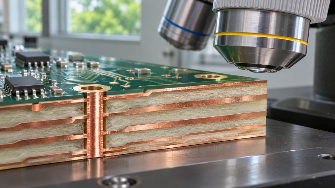
A stripline is a conductor embedded between two reference planes. In a symmetric geometry the trace has equal dielectric spacing to those planes; in an offset geometry it does not. Analog Devices’ layout guide explains why the dielectric dimensions matter to stripline impedance.
Why the Total Gap Does Not Describe the Geometry
Adding the upper and lower clearances hides where the trace sits. Moving the same trace toward one plane changes the field distribution and coupling. Preserve both individual dimensions in the impedance model rather than using their sum as the only spacing input.
Detailed Stackup Inputs to Collect
| Item | Unit or record | Purpose |
| Upper dielectric | Finished distance in mm | Describes the upper field region |
| Lower dielectric | Finished distance in mm | Describes the lower field region |
| Trace width and thickness | Finished geometry in mm | Sets conductor cross-section |
| Dielectric properties | Model value and frequency | Represents each dielectric region |
| Reference layers | Layer IDs and net | Establishes the physical structure |
Symmetric vs Offset Stripline
| Input | Symmetric example | Offset example |
| Upper clearance | 0.15 mm | 0.10 mm |
| Lower clearance | 0.15 mm | 0.20 mm |
| Sum of clearances | 0.30 mm | 0.30 mm |
| Model choice | Symmetric geometry | Preserve both distances |
Worked Example: Same Sum, Different Input
The two examples in the table have the same total dielectric clearance, but the trace in the second sits 0.05 mm closer to the upper plane. Keep the copper thickness and material assumptions explicit. The example compares model inputs only; it does not predict an impedance value.
Know What the Published Formula Assumes
Analog Devices’ symmetric stripline handbook section describes a trace between equally spaced reference planes. Its symmetric expression is not a substitute for a model of an off-centre trace. Use the formula only within the geometry and assumptions it describes.
Account for Copper Thickness in the Datum
Confirm whether the two distances are measured from the trace faces, its centreline, or another reference. When using face-to-plane dielectric clearances, the complete plane separation also includes the conductor thickness. Do not add thickness twice when converting the drawing to solver inputs.
Check Which Materials Sit Above and Below
Even equal clearances do not make every electrical property symmetric if the dielectric constructions differ. Record the material on each side, along with relevant properties and frequency assumptions. The solver should represent the chosen construction rather than assuming one material throughout.
Recalculate When the Fabricator Proposes a New Stackup
A proposed replacement can keep overall board thickness while changing one of the local distances. Ask for the approved finished dimensions, re-evaluate trace width or pair spacing if needed, and check whether the existing routing still fits the required clearances.
Use a Coupon That Represents the Offset Layer
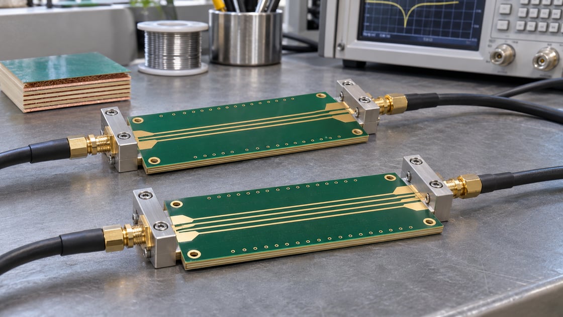
Match the routed layer, upper and lower references and relevant conductor geometry. A coupon on another layer may answer a different question. Agree on how the result will be measured and which dimensions are checked when a result falls outside its target.
Check Transitions Separately
A uniform stripline model does not describe every connector or via transition. Review how reference current transfers where the route changes layers. The BestPCBs impedance control guide covers the wider stackup and test handoff.
Document Both Clearances Before Release
Record the layer pair, two dielectric distances, conductor dimensions, model assumptions and acceptance evidence. Keep the coupon associated with that revision. If the two distances are not known, leave the impedance estimate provisional rather than converting an assumed stackup into an approved requirement.
Discuss an Impedance Stackup
Send the layer map and controlled geometries to Best Technology.
FAQ
Can I use the average of the two clearances?
Not as a final model for an offset stripline. Averaging discards the location of the trace between the planes. Use the actual upper and lower distances and an appropriate model, then compare the result with representative evidence if the design requires a controlled impedance.
Does equal plane spacing guarantee equal impedance?
No. Trace position, dimensions and dielectric properties matter even when the total distance between planes is the same. Keep the individual distances in the input record. Compare complete geometries rather than using a matching total as proof that two fabricated builds are electrically equivalent.
Can the two sides use different dielectric constructions?
A stackup may have different constructions on either side, but the model and fabrication review must account for them. Record both materials and their relevant properties. Do not use a single bulk dielectric input unless that approximation is justified for the electrical requirement and confirmed where necessary.
Is offset stripline necessarily worse than symmetric stripline?
No. It is a different geometry with different constraints and can be intentional. Compare impedance, available routing and reference continuity for the actual design. A symmetric structure may simplify the initial calculation, but suitability still depends on the requirements and on what can be built consistently.
Can I keep the same trace width after a stackup change?
Only after verifying that the new geometry meets the required impedance and layout constraints. A change in either dielectric distance can matter. Recheck the model and approved construction first, and decide whether the fabrication data or artwork needs updating before placing a production order.
Does an impedance coupon verify every transition?
No. A coupon for a uniform trace does not necessarily include the vias, launches or reference changes in the actual channel. Define which structures the coupon represents and decide whether the transitions need a separate model, test structure or assembled board measurement for the application.
Do I measure spacing from the trace centre or its face?
Use the convention required by the solver or drawing and convert dimensions consistently. A face-to-plane dielectric gap is not the same as a centreline-to-plane dimension. State the convention in the handoff and account for copper thickness exactly once when combining the measurements.
What should I ask the fabricator to confirm?
Ask for the finished upper and lower spacing, copper geometry, applicable material inputs and coupon layer. Include the target impedance and tolerance. Confirm the agreed measurement method and keep the answer linked to the actual artwork and stackup revision that will be released.