Asymmetric copper in PCB design means that copper is not mirrored evenly across the board. The asymmetry may come from different copper weights on paired layers, unequal copper coverage on opposite layers, or a stackup whose copper and dielectric construction is not balanced around the centerline. These are related conditions, but they are not interchangeable. A board can use several copper weights and still remain symmetric, while a board made from one copper weight can become asymmetric after most of the copper is etched away from only one side.
What Is the Structure of Asymmetric Copper?
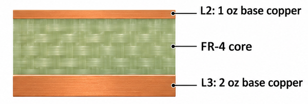
In its most direct core-level form, asymmetric copper uses one dielectric core with different base copper weights on its two faces. For example, one face may use 1 oz copper while the opposite face uses 2 oz copper. In a complete multilayer PCB, the term also covers unequal copper coverage and non-mirrored copper positions, but the unequal-clad core is the clearest physical structure.
The core cross-section below is a schematic and is not drawn to scale. The front and back labels describe a fixed drawing orientation; the released stackup must identify the actual layer numbers so the core cannot be reversed during preparation.
Common asymmetric copper combinations include:
| Copper combination | Front side | Back side |
|---|---|---|
| 0.5 oz / 1 oz | Approx. 17.5 µm | Approx. 35 µm |
| 1 oz / 2 oz | Approx. 35 µm | Approx. 70 µm |
| 1 oz / 3 oz | Approx. 35 µm | Approx. 105 µm |
| 2 oz / 3 oz | Approx. 70 µm | Approx. 105 µm |
These are nominal communication values rather than finished-copper tolerances. The production drawing still needs to state the required base copper, finished copper and applicable tolerance for each layer.
| Form of asymmetry | What is different | Typical design evidence | Main manufacturing concern |
|---|---|---|---|
| Copper weight asymmetry | Paired or opposing layers use different base copper weights | Stackup table lists different oz/ft² or µm values | Etch capability, material availability and mechanical balance |
| Copper coverage asymmetry | One side or region retains much more copper after etching | Gerber or ODB++ artwork shows a plane opposite sparse routing | Resin flow, plating distribution and bow or twist |
| Stackup asymmetry | Copper and dielectric layers are not mirrored about the board centerline | Layer order, dielectric thickness or copper position differs above and below the center | Uneven mechanical and thermal response |
The phrase therefore describes a design condition, not a single material grade. The fabrication data must show which type is intended before we can assess it.
Where Can Copper Asymmetry Appear in a PCB?
Copper asymmetry can appear between the two faces of a copper-clad core, between mirror layers of a multilayer board, across different regions of one layer, or between the top and bottom halves of the complete stackup. Each location creates a different review task.
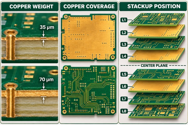
For example, unequal cladding on a core is a material and orientation issue. Unequal copper coverage is primarily an artwork and process-distribution issue. A non-mirrored multilayer construction is a stackup issue even when every individual foil starts at the same thickness. Treating all three as “different copper thickness” hides the actual source of risk.
Why Is Copper Symmetry Preferred in Multilayer PCBs?
Copper symmetry is preferred because it gives the laminate a more balanced structure during pressing, etching, plating, cooling and assembly. Copper, glass reinforcement and resin do not respond identically to process temperature. When the board is strongly unbalanced, the internal forces generated during heating and cooling are also less balanced.
Symmetry also simplifies manufacturing control. Mirror layers with comparable copper weight and coverage demand similar resin filling, etching and dimensional compensation. This does not mean every circuit must be perfectly mirrored. It means any intentional departure should solve a real electrical or mechanical constraint and should be reviewed as part of the complete stackup.
Why Is Asymmetric Copper Used in PCB Design?
Asymmetric copper is used when the circuit cannot meet its electrical or mechanical requirements with a practical symmetric construction. One layer may need heavier copper for a width-limited power path while its opposing layer needs finer features. A rigid-flex transition, embedded structure or application-specific layer sequence may also prevent a perfectly mirrored build.
The design should first test whether routing changes, a wider conductor, a different layer assignment, or a symmetric heavy-copper pair can solve the same problem. If those options increase layer count, block fine-pitch escape routing or create a worse constraint, the asymmetric construction becomes a deliberate engineering choice rather than an accidental imbalance.
Asymmetric Copper vs Standard PCB: What Is the Difference?
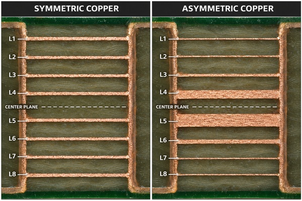
For this comparison, a standard PCB means a conventional balanced construction whose paired copper weights, copper positions and dielectric structure are mirrored around the centerline. Asymmetric copper deliberately leaves one or more of those elements unmatched to solve a specific design requirement.
| Review item | Standard balanced PCB | Asymmetric copper PCB |
|---|---|---|
| Stackup planning | Mirror layers normally use comparable copper and dielectric construction | Every unmatched layer or copper condition needs a stated reason |
| Etching | Paired layers are more likely to share similar process demand | Heavy and fine-feature layers may require separate compensation or process review |
| Lamination | Resin demand and mechanical response are easier to balance | Copper-free area, copper thickness and layer position require closer review |
| Flatness | Symmetry helps reduce one source of bow and twist | Flatness risk depends on the full construction and artwork distribution |
| Inspection | Standard stackup verification may be sufficient | Layer identity, copper thickness and orientation need explicit records |
| Best use | General multilayer construction and repeatable production | Designs with a documented requirement that a symmetric stack cannot satisfy |
For a conventional multilayer PCB, we normally begin with a balanced stack and move to an asymmetric one only when the circuit requirement is clear.
What Is Asymmetric Copper Thickness?
Asymmetric Copper Thickness is the thickness-specific form of asymmetric copper. It means that designated layers or paired faces do not use the same base or finished copper thickness. The drawing must distinguish base foil from finished copper because plating changes the outer-layer result, while inner layers are primarily defined by their starting foil and subsequent processing.
| Parameter to specify | Unit or format | Why it matters | Where to record it |
|---|---|---|---|
| Layer identity | L1, L2, L3, etc. | Prevents “top/bottom” orientation errors | Controlled stackup drawing |
| Base copper weight | oz/ft² or µm | Determines the starting foil and etch depth | One value for every copper layer |
| Finished copper requirement | Minimum or nominal µm | Separates required result from starting foil | Fabrication notes and acceptance criteria |
| Copper coverage | Percentage or artwork review | Indicates resin and plating distribution demand | Gerber/ODB++ analysis and DFM record |
| Minimum line and space | mil or mm by layer | Links copper thickness to etch feasibility | Layer-specific design rules |
| Dielectric construction | Material, core/prepreg and thickness | Defines spacing, resin supply and mechanical balance | Stackup table |
| Impedance requirement | Target and tolerance | Connects finished geometry to electrical performance | Controlled-impedance table |
| Bow and twist limit | Agreed percentage and method | Converts flatness concern into a measurable requirement | Drawing or quality plan |
Nominal conversions such as 1 oz/ft² being approximately 35 µm are useful for communication, but the released drawing should use the layer-specific values agreed for production. A list of example copper pairs is not a substitute for the actual stackup.
What Makes Asymmetric Copper Difficult to Manufacture?
The main production difficulty is that the two sides or paired layers do not respond to the same process conditions in the same way. We must preserve the intended core orientation, apply layer-specific etch compensation, evaluate resin demand against copper coverage, control plating distribution and verify flatness after the full board construction is complete.
| Production stage | Main difficulty | Manufacturing control |
|---|---|---|
| Material preparation | Unequal-clad cores can be reversed if layer identity is unclear | Match the core orientation to fixed layer numbers in the approved stackup |
| Imaging and etching | Thick copper needs a different etch allowance from thin copper and fine features | Review minimum line and space separately for each copper layer |
| Lamination | Unequal copper coverage changes resin demand and mechanical balance | Review copper-free area, prepreg resin supply and stack symmetry together |
| Electroplating | Sparse and dense areas can receive different current density | Check local copper density and use approved balancing features where appropriate |
| Final inspection | Continuity alone cannot confirm copper thickness, orientation or flatness | Combine thickness measurement, microsection, impedance and bow-and-twist checks as required |
Etching, plating, flatness and final inspection require separate controls because each responds to different design data and uses a different acceptance method.
How Does Copper Weight Affect Etching?
Heavier copper requires the etchant to clear a deeper metal layer. During that time, lateral etching also changes the conductor sidewalls. As copper thickness increases, the available line-and-space window usually becomes more demanding, especially when the same layer contains fine gaps and large copper areas.
This is why a heavy copper PCB cannot be reviewed only by current requirement. We also check the smallest conductor, the narrowest clearance, pad geometry, layer position and whether the drawing refers to base or finished copper. An asymmetric design may be workable, but the heavy layer and the fine-feature layer should not automatically share one design rule.
How Does Copper Coverage Affect Electroplating?
Copper coverage affects how current is distributed during electroplating. Sparse and dense regions can plate at different rates, so the finished copper thickness may vary more across a poorly balanced panel. The issue is different from starting foil weight: two layers may begin with equal foil and still have very different plating behavior because their retained copper patterns are not alike.
At DFM, we compare local copper density, large open areas, isolated features and panel distribution. Copper thieving or other non-functional balancing features may improve process uniformity, but they must respect electrical clearance, impedance, creepage and customer restrictions.
How Does Asymmetric Copper Affect PCB Bow and Twist?
Asymmetric copper can contribute to bow and twist because the board develops a less balanced mechanical response during lamination and later thermal cycles. The risk increases when copper thickness, copper coverage and dielectric construction are all unbalanced in the same direction.
However, one unmatched copper value does not predict the finished flatness by itself. Board size, thickness, material, panel layout, retained copper pattern, press construction and assembly temperature also matter. The correct review is therefore the complete stackup and artwork, followed by measurement against an agreed finished-board requirement.
How Does Asymmetric Copper Affect Controlled Impedance?
Asymmetric copper affects controlled impedance when it changes conductor thickness, etched width, dielectric spacing or the reference-plane relationship. Two traces with the same drawn width do not necessarily produce the same impedance if they are made on different copper weights or use different dielectric environments.
For an impedance control PCB, the impedance table should identify the signal layer, reference layer, target, tolerance and intended finished geometry. We calculate and review each controlled structure in its actual stackup instead of copying one trace width across asymmetric layers.
How Does It Affect Current and Heat Distribution?
Thicker copper provides more conductor cross-section, which can reduce DC resistance for the same length and width. That benefit applies to the specific path that receives the extra copper; it does not automatically increase the current capacity of vias, connectors, solder joints or narrow necks elsewhere in the circuit.
Heat distribution is equally path-dependent. A copper-rich plane can spread heat laterally, while a sparse opposing layer may not provide the same thermal path. We therefore review the whole current loop and heat path rather than treating copper weight as a board-level rating.
How Should a Stackup Show Asymmetric Copper?
The stackup should identify every copper layer, base copper value, dielectric layer, material type and finished board thickness in one fixed viewing direction. If a core uses unequal cladding, the drawing should state which copper face belongs to which layer. Terms such as “heavy side down” are too easy to reverse when a panel is turned.
The stackup should also separate copper weight from artwork coverage. A note that says “2 oz power layer” does not show whether the layer is a solid plane, a sparse routing layer or a mixture of both. Gerber or ODB++ data must accompany the stackup so the physical build and actual pattern can be reviewed together.
How Can Copper Thieving Improve Balance?
Copper thieving adds non-functional copper to selected empty regions so plating and copper distribution become more uniform. It can help when a layer has large copper-free areas or when opposite regions of the panel are strongly unbalanced.
Thieving is not a universal repair. It must not violate creepage, clearance, RF keepouts, antenna zones, isolation requirements or customer rules for unused copper. It also cannot turn a fundamentally non-mirrored stackup into a symmetric one. The feature should be agreed during DFM and clearly separated from functional circuitry.
How Do We Inspect Asymmetric Copper Boards?
We inspect asymmetric copper boards by linking the released stackup to material issue, layer identity and finished verification. The inspection plan may include artwork review, copper-thickness measurement, microsection analysis, impedance testing and bow-and-twist measurement, depending on which requirements are critical to the design.
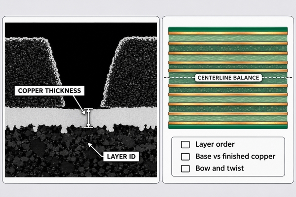
A microsection is useful only when the measured location and layer are identified. Measuring a copper-free clearance does not verify the conductor thickness on that layer. Likewise, an electrical continuity test cannot prove that an unequal-clad core was oriented correctly. Each acceptance method must answer the requirement it is intended to verify.
What Should You Send for DFM Review?
Send the complete stackup, Gerber or ODB++ data, drill files, board outline and fabrication drawing. Mark base and finished copper requirements by layer, identify controlled-impedance structures, state critical line/space values and include the required flatness or thickness limits when they affect assembly.
EBest Circuit (Best Technology) can review asymmetric copper constructions for FR4 PCB, multilayer, heavy-copper and impedance-controlled projects. For quotation and DFM review, send the released files, order quantity and application constraints to sales@bestpcbs.com. We will review the intended asymmetry against the complete build instead of assuming that one copper value describes the whole board.