PCB manufacturing PCB manufacturing
Home > Blog

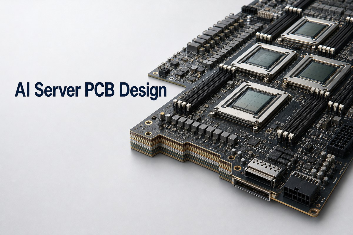
AI Server PCB Design

Best AI Server PCB Manufacturer From Design to Assembly
Tuesday, August 11th, 2026

An AI Server PCB project succeeds when its electrical and mechanical requirements survive every handoff from architecture and layout to fabrication, assembly, and testing. The central task is to preserve signal, power, thermal, and mechanical margin in a construction that can be manufactured repeatedly.

Before layout begins, define the board’s role, interface generations, power profile, cooling conditions, connector locations, mechanical limits, and acceptance tests. These inputs determine the materials, stackup, via structure, manufacturing controls, and quotation scope.

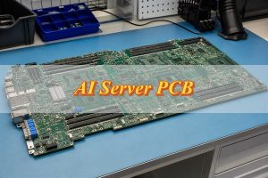
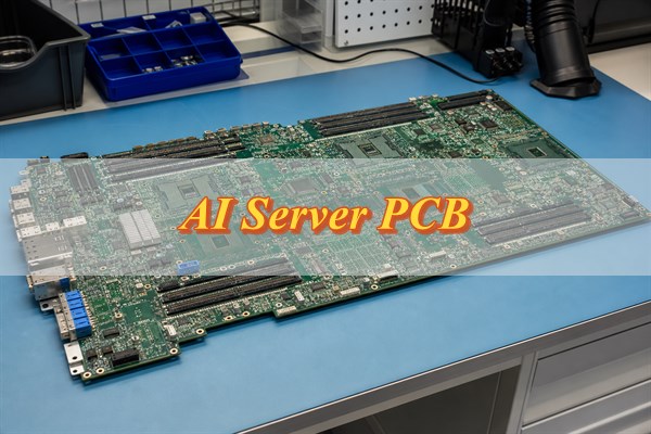
AI Server PCB manufacturing review on a large server-class circuit board

What Is an AI Server PCB?

An AI server PCB is a circuit board that carries one or more compute, memory, networking, storage, control, or power functions inside an AI server. Fast interfaces, concentrated power, dense packages, large board formats, and continuous workloads make these boards more demanding than their basic copper-and-dielectric construction suggests.

The term can refer to a host motherboard, accelerator baseboard, network switch board, power distribution board, backplane, or management board. Requirements depend on the processors, interfaces, power rails, connectors, and cooling conditions assigned to that board. Defining its role gives the designer and manufacturer a sound basis for the stackup, materials, via structure, and test plan.

Which PCB Boards Are Used in an AI Server?

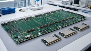
An AI server normally uses several PCB boards to perform different system functions. The exact combination depends on the server architecture; common board types are listed below.

PCB Board Primary Function
Host motherboard Connects the CPU, memory, storage, management controller, and expansion devices
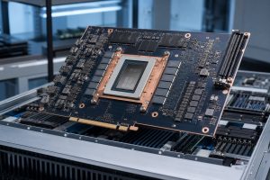
Accelerator baseboard Connects GPUs or other accelerator modules and supports communication between them
Network or switch board Transfers data between accelerators, servers, and external networks
Power distribution board Distributes or converts power for processors, accelerators, and other server loads
Backplane Connects multiple server boards, storage devices, or modules through a shared interface
Riser board Changes the orientation or position of expansion cards within the server chassis
Management board Monitors server status and supports remote control, diagnostics, and system management
Storage board Connects and controls SSDs, hard drives, or other storage devices

Not every AI server uses every board listed above. Some functions may be combined on one PCB, while modular platforms may separate them across several boards. Identifying the board type and its function prevents a host motherboard, accelerator baseboard, backplane, or power board from being quoted as though they were the same product.

How Is an AI Server PCB Different from a Standard Server PCB?

An AI server PCB differs from a standard server PCB mainly in accelerator connectivity, local power demand, routing density, cooling loads, and the validation needed to prove stable operation. The exact difference depends on the server architecture, but the board-level comparison below shows the usual design shift.

Comparison Area Standard Server PCB AI Server PCB
Board architecture Primarily connects CPUs, memory, storage, management, and network interfaces Adds dense GPU or accelerator modules and the high-bandwidth fabric that connects them
High-speed routing Channel count and routing density follow conventional server interfaces More simultaneous accelerator and fabric links increase breakout, reference-plane, via-transition, and crosstalk constraints
Power delivery Power planes and regulators support conventional processor, memory, storage, and network loads Higher localized current and faster load changes near accelerators demand lower-impedance power paths, stronger decoupling, and closer thermal review
Materials and stackup High-Tg FR-4 or other materials may be sufficient when the verified channel budget allows Long or fast accelerator links may require lower-loss laminate, tighter impedance control, shorter stubs, and additional routing or power-distribution layers
Thermal and mechanical design Board support and cooling are sized for the standard component and heat-sink arrangement Large packages, heavier cooling hardware, concentrated heat, and connector density increase the need to control board support, airflow, bow, twist, and mating alignment
Validation scope Bare-board, assembly, functional, and platform tests confirm the specified server design Validation must also correlate channel margin, power behavior, temperature, mechanical fit, and workload stability across the accelerator platform

A standard server stackup should therefore be reused only after its channel loss, reference planes, power distribution, via structure, board support, and thermal margin have been checked against the AI server architecture.

Why Does an AI Server PCB Need High-Speed and High-Power Design?

An AI server PCB needs high-speed design to move large amounts of data between processors, memory, accelerators, storage, and network interfaces, and it needs high-power design to deliver stable current to those devices under rapidly changing workloads. If either side is inadequate, the server may lose interface margin, suffer voltage instability, overheat, or throttle before it reaches its intended performance.

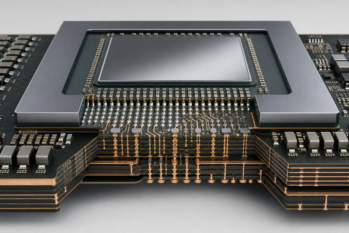
High-speed design protects signal integrity. Package escape, trace geometry, dielectric loss, copper roughness, vias, reference-plane transitions, connectors, and module interfaces all contribute to channel loss and reflections. The PCB therefore needs controlled impedance, continuous return paths, appropriate materials, and transition structures that keep the complete channel within its electrical budget.

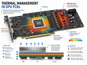
High-power design protects power integrity and temperature margin. Accelerators can draw high local current and change load quickly, so power planes, copper distribution, vias, voltage regulators, and decoupling must limit voltage drop and transient noise while carrying current without excessive heating.

The two requirements must be reviewed together. Dense signal routing can reduce the space available for power copper, while plane splits, large via fields, and copper imbalance can affect return paths, lamination, and thermal behavior. The design target is sufficient signal and power margin under the intended workload and operating temperature—not maximum performance in only one domain.

How Should an AI Server PCB Be Designed?

An AI server PCB should be designed in a controlled sequence from system requirements to a verified production package. Signal, power, thermal, mechanical, manufacturing, and test decisions must be developed together because a change in one area can reduce margin in another.

  1. Define the board role: Identify whether the PCB is a host motherboard, accelerator baseboard, network board, power board, backplane, riser, management board, or storage board, then define its interfaces with the rest of the server.
  2. Set measurable constraints: Record interface generations and channel budgets, rail voltages and current profiles, board outline, connector locations, component heights, cooling zones, mounting points, and required validation results.
  3. Select materials and stackup: Choose laminates, copper weights, layer functions, reference planes, impedance structures, and via types that meet electrical and reliability needs while remaining manufacturable.
  4. Place critical components: Position processors, accelerators, memory, regulators, clocks, connectors, and decoupling parts to shorten sensitive paths, support airflow, and leave realistic breakout and assembly space.
  5. Design the power distribution network: Size planes, pours, vias, regulator connections, and decoupling for DC voltage drop, transient response, current density, and temperature rise at the expected workload.
  6. Route high-speed interfaces: Maintain controlled impedance and continuous return paths, limit discontinuities and stubs, manage lane spacing and length requirements, and review packages, vias, connectors, and cables as one channel.
  7. Review thermal, mechanical, and DFM risks: Check copper balance, heat-sink and board-support loads, airflow, warpage, connector alignment, drill and registration limits, assembly access, and test-point availability.
  8. Verify and release the design: Close signal, power, thermal, mechanical, DFM, and test findings, then issue one synchronized revision of the fabrication data, drawings, stackup, netlist, BOM, assembly files, and acceptance criteria.

Which Materials and Stackups Are Suitable for an AI Server PCB?

AI server PCBs typically use high-Tg FR-4, mid-loss laminate, or low-loss high-speed laminate, selected according to the function and channel budget of each board. Accelerator baseboards and network or switch boards usually need the lowest-loss construction. Host motherboards often combine high-speed routing with substantial power distribution. Management and lower-speed storage boards may use high-Tg FR-4 when verified channel loss remains within the interface budget.

AI Server PCB Type Suitable Material Direction Stackup Priorities
Accelerator baseboard Low-loss laminate with controlled dielectric properties and low-profile copper for long, fast processor-to-processor or processor-to-module links Critical signal layers beside continuous ground references, short via transitions, sufficient power and ground planes, and balanced copper distribution
Network or switch board Low-loss high-speed laminate selected from the total connector, via, and trace loss budget Closely referenced differential-pair layers, controlled breakout and backdrill structures, isolation between channel groups, and stable return paths through connectors
Host motherboard Mid-loss or low-loss laminate for high-speed regions, with high-Tg and reliability characteristics suitable for the complete board Separate routing, reference, and power-distribution functions; enough breakout layers for dense packages; and plane pairs positioned to support return current and decoupling
Power distribution board High-Tg laminate with copper thickness and thermal behavior matched to the required current; low-loss dielectric is usually not the primary need Wide copper areas, parallel power and ground paths, adequate via arrays, thermal balance, insulation spacing, and mechanical support for high-current connections
Backplane or riser Mid-loss or low-loss laminate when it carries high-speed fabrics; high-Tg FR-4 may suit lower-speed control or power-only connections Connector-launch control, continuous references, short transitions, mechanical thickness control, and balanced construction for mating alignment
Management or storage board High-Tg FR-4 for moderate-speed functions, upgraded to a mid-loss material when interface length and speed require more channel margin A simpler multilayer stackup with clear signal references, practical power planes, manufacturable vias, and enough test access

The layer count should not be chosen from the term ā€œAI serverā€ alone. It is determined by package escape, routing density, reference-plane continuity, current distribution, board thickness, via aspect ratio, and mechanical balance. Adding layers without assigning each one a necessary function increases cost and fabrication difficulty without guaranteeing better electrical performance.

Final material approval should be based on the complete channel and construction. Confirm dielectric data at the relevant frequency, copper profile, glass style, resin system, thermal expansion, CAF resistance, availability, pressed thickness, impedance geometry, and fabricator capability. If two laminate families are combined, their bonding, drilling, registration, and thermal compatibility must be reviewed before release.

What Should Be Checked During an AI Server PCB DFM Review?

An AI server PCB DFM review should check the stackup, via architecture, registration margin, copper balance, assembly geometry, and test access against both factory capability and the board’s electrical and mechanical intent. A minimum trace-and-space check alone cannot reveal whether the complete construction is manufacturable.

  • Stackup definition: Confirm material designations, pressed dielectric thicknesses, copper weights, impedance structures, finished board thickness, and permitted material alternatives. The fabrication drawing, impedance table, and layer data must describe the same construction.
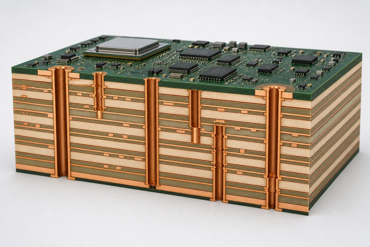
  • Via architecture: Review drill sizes, finished hole sizes, aspect ratios, annular rings, capture pads, drill-to-copper clearances, laser-via cycles, buried vias, and backdrill depths as one interconnection system.
  • Registration margin: Check that fine-pitch escapes, dense via fields, plane clearances, and backdrill targets retain enough tolerance for imaging, lamination, and drilling variation.
  • Impedance and return paths: Match the proposed trace geometries to the approved stackup and confirm that reference planes remain continuous through layer changes, connector launches, and high-density breakout regions.
  • Copper and mechanical balance: Review local copper density, plane distribution, board thickness, panel orientation, heavy components, and heat-sink loads to reduce plating variation, bow, twist, and assembly distortion.
  • Assembly geometry: Verify pad and solder-mask geometry, component spacing, polarity markings, stencil-sensitive packages, board support, inspection visibility, and rework access against the intended assembly process.
  • Test access: Reserve usable access for bare-board electrical test, impedance coupons, programming, boundary scan, functional fixtures, and measurement points required by the acceptance plan.

The DFM report should separate mandatory corrections from optional improvements and accepted exceptions. Any proposal that changes impedance, current capacity, timing, thermal paths, component fit, or connector alignment requires documented design approval before fabrication data is released.

How Does AI Server PCB Prototyping Reduce Production Risk?

AI server PCB prototyping reduces production risk by testing the assumptions that control yield, performance, assembly, and system fit before they are repeated across a production lot. A useful prototype build supports six release decisions.

  1. Verify the PCB construction: Measure finished thickness, impedance coupons, microsections, annular rings, backdrill results, bow and twist, and electrical continuity. Use the results to confirm or correct the stackup, drill structure, plating requirements, impedance geometry, and panel process.
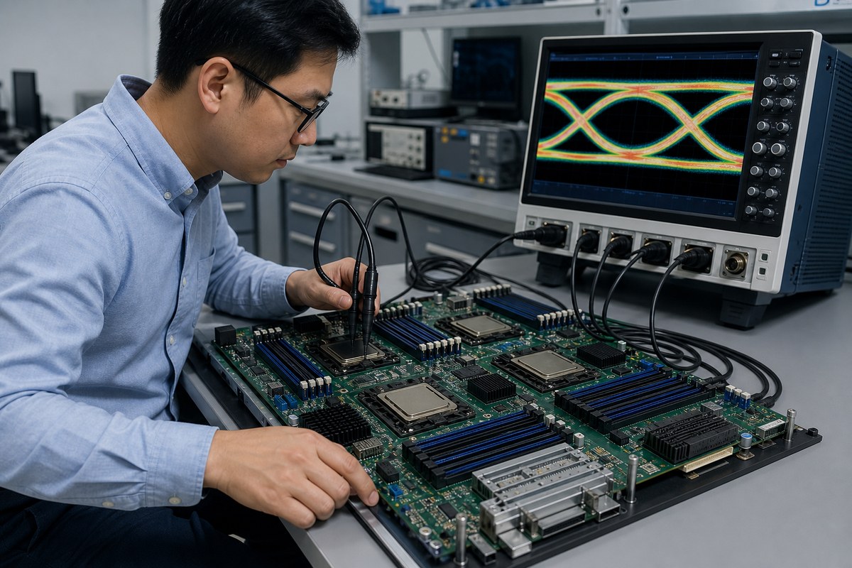
  2. Validate high-speed channels: Review link training, eye or margin results, error behavior, and measurements across traces, vias, and connectors. Release the channel only when routing, reference transitions, via stubs, connector launches, and material loss provide sufficient margin.
  3. Prove power delivery: Measure rail sequence, voltage drop, ripple, transient response, current sharing, and temperature at the expected load. Adjust planes, via arrays, decoupling, regulator settings, copper distribution, or cooling where limits are missed.
  4. Check mechanical and thermal fit: Inspect connector alignment, module seating, heat-sink contact, board support, airflow clearance, and operating temperature. Correct the outline, mounting, stiffening, connector position, cooling interface, or chassis tolerance before production.
  5. Qualify the assembly process: Review the first article, AOI, X-ray, solder joints, component coplanarity, and measured reflow profile. Refine stencil apertures, paste volume, support tooling, placement, reflow settings, inspection scope, or rework access as required.
  6. Confirm test and traceability: Verify fixture access, programming, functional logs, serial and lot records, BOM revision, and failure disposition. Finalize test coverage, acceptance limits, fixture controls, data retention, and repeat-order records before release.

Production release requires every prototype finding to have a recorded disposition. The issue must be corrected and retested, accepted with a documented limit, or transferred into a controlled production inspection or test. This prevents an unresolved prototype anomaly from becoming a repeated lot-level failure.

How Is an AI Server PCB Manufactured?

An AI server PCB is manufactured by building and inspecting its inner layers, laminating them into a multilayer panel, forming plated interconnections, completing the outer surfaces, and verifying the finished bare board against the released data. Controls are applied at each stage because buried defects cannot be corrected after the structure is complete.

  1. Engineering and CAM review: Reconcile artwork, netlist, drawings, stackup, controlled-impedance features, drill data, materials, tolerances, and revision identifiers before panelization.
  2. Material preparation: Verify cores, prepregs, and copper foils, then clean and prepare them according to the approved stackup and material-lot controls.
  3. Inner-layer formation: Image, develop, etch, and strip the internal circuitry, then use AOI to find opens, shorts, neck-down, and pattern defects before the layers are buried.
  4. Layup and lamination: Align the inspected cores with prepregs and copper foils, then press the panel while controlling registration, resin flow, pressure, temperature, and finished thickness.
  5. Drilling and hole preparation: Drill plated through-holes and backdrill features as specified, laser-drill microvias where required, then remove resin smear and condition the hole walls. Buried vias are formed within their designated subassemblies before final lamination.
  6. Copper deposition and plating: Deposit conductive copper in the holes and plate them to the specified thickness. Sequential build-up boards repeat imaging, lamination, drilling, and plating for each defined cycle.
  7. Outer-layer formation: Apply the outer-layer image, plate the required copper and etch resist, remove unwanted copper, and inspect the completed external circuitry.
  8. Solder mask and surface finish: Apply and cure solder mask with controlled registration, add permitted markings, and form the specified finish on exposed pads.
  9. Profiling and cleaning: Route, score, or otherwise form the final board and panel features, then remove process residues and verify critical dimensions and connector features.
  10. Final bare-board verification: Perform electrical test, dimensional and visual inspection, impedance testing, and any specified microsection or construction checks before final identification, packaging, and release.

Traceability should connect the finished AI Server PCB to its revision, material lots, process route, approved deviations, and test records. These records establish the manufacturing baseline for repeat orders and failure investigation.

What Does AI Server PCB Assembly Require?

AI server PCB assembly requires accurate component data, controlled material handling, stable board support, package-specific soldering, a measured thermal profile, and first-article approval. The assembly process should be defined around the actual board and component mix rather than a generic SMT recipe.

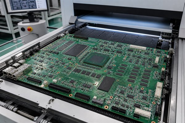
AI Server PCB assembly on an automated inspection conveyor
  1. Release one consistent assembly package: Align the BOM, manufacturer part numbers, centroid data, assembly drawings, polarity marks, approved substitutions, and PCB revision before components are issued to production.
  2. Control component condition: Verify packaging, lot identification, moisture sensitivity, floor life, baking requirements, solderability risk, and quantities for factory-sourced and customer-supplied parts.
  3. Support the PCB during processing: Use suitable carriers, rails, or fixtures for large, heavy, thin, or densely populated boards so that printing, placement, reflow, and handling do not introduce excessive flex or warpage.
  4. Match solder paste to the package mix: Set stencil thickness, aperture design, paste type, and print parameters for fine-pitch devices, large thermal pads, connectors, BGAs, and components with different solder-volume needs.
  5. Control placement and special assembly steps: Confirm feeder setup, package orientation, placement force, connector seating, press-fit operations, through-hole insertion, hand soldering, and any required heat-sink or hardware installation.
  6. Develop a measured thermal profile: Attach thermocouples to representative high-mass and temperature-sensitive locations, then set preheat, soak, peak temperature, time above liquidus, and cooling conditions for the populated board.
  7. Approve the first article before continuing: Verify component identity, orientation, placement, solder joints, mechanical fit, and required rework on the first completed unit before releasing the remaining build quantity.

How Is AI Server PCB Quality Inspected and Tested?

AI server PCB quality is inspected throughout fabrication and assembly, then verified through electrical and functional testing before release. Each stage targets defects that may become hidden or more expensive to correct later.

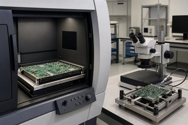
AI Server PCB quality inspection with X-ray and optical equipment
  1. Verify materials and production data: Match laminate, prepreg, copper, surface finish, stackup, drill files, netlist, impedance requirements, and revision identifiers to the released order before fabrication begins.
  2. Inspect inner layers before lamination: Use AOI and dimensional checks to detect opens, shorts, conductor damage, incorrect clearances, and registration problems while the circuitry is still accessible.
  3. Control lamination, drilling, and plating: Monitor pressed thickness, layer alignment, hole position, desmear, copper deposition, and plating. Microsections can verify hole-wall copper, interconnection quality, dielectric thickness, and backdrill results where specified.
  4. Test the finished bare board: Perform electrical testing against the supplied netlist, inspect dimensions and workmanship, and verify controlled impedance with the agreed coupons. Additional checks may cover bow and twist, solder-mask registration, surface finish, and final hole size.
  5. Inspect the assembled PCB: Confirm the first article against the BOM, placement data, drawings, polarity, and component orientation. SPI checks solder-paste deposition, AOI examines visible placement and solder features, and X-ray evaluates hidden joints beneath packages.
  6. Run electrical and functional tests: Apply the approved procedure for continuity, shorts, rail sequence, voltage limits, programming, communications, interfaces, and board functions. Each test needs defined limits, recorded results, and a disposition for failures.
  7. Review records before release: Link the shipped boards to their revision, material and component lots, inspection results, test logs, repairs, and approved deviations. Release only units that meet the agreed acceptance criteria.

Factory testing verifies the PCB and assembled board within the agreed test scope; it does not automatically qualify the complete AI server. Firmware, cooling, chassis interaction, workload stability, and full-system performance require validation in the customer’s final platform.

Why Choose EBest Circuit as Your AI Server PCB Manufacturer?

One source from design support to assembled production. EBest Circuit combines PCB design, prototyping, production, component sourcing, and assembly.

  • One accountable supplier: Customers coordinate design support, PCB fabrication, component sourcing, assembly, and production questions through one company instead of managing several disconnected vendors.
  • Lower prototype-transfer risk: EBest supports both prototypes and mass production, allowing approved stackups, revisions, BOM decisions, and inspection requirements to carry into repeat builds.
  • Better technology fit: Available capabilities include multilayer, high-Tg, high-speed, impedance-controlled, HDI, and heavy-copper PCBs for different signal, power, density, and thermal requirements.
  • Earlier engineering review: PCB design support and fabrication are coordinated so that material, stackup, via, impedance, and manufacturability issues can be addressed before release.
  • Simpler component coordination: EBest combines component sourcing with PCB assembly, helping customers manage approved parts, substitutions, consigned components, and shortages within the same project.
  • Documented quality qualifications: EBest’s qualifications include ISO 9001:2015, ISO 13485:2016, IATF 16949, AS9100D, UL, RoHS, and REACH; customers can confirm the scope required for their order.
  • Long-term manufacturing support: Established in 2006, EBest supports custom PCB projects and offers expedited service when the selected materials, processes, components, and inspection requirements allow it.

What Files Are Needed for an AI Server PCB Quotation?

For an accurate AI server PCB quotation, provide five groups of information. Complete inputs prevent conflicting assumptions about fabrication, assembly, testing, and delivery.

  • PCB files: Gerber, ODB++, or IPC-2581 data, plus NC drill files, netlist, board outline, and fabrication drawing.
  • Build requirements: Stackup, materials, copper weights, finished thickness, impedance, via structure, surface finish, tolerances, and acceptance standard.
  • Assembly files: BOM with manufacturer part numbers, centroid data, assembly drawings, polarity information, and special handling notes.
  • Test scope: Required bare-board tests, impedance coupons, programming, functional procedure, acceptance limits, fixtures, and reports.
  • Order details: Prototype and production quantities, requested delivery date, consigned parts, approved substitutions, packaging, and destination.

Use the same revision identifier across every file and clearly mark any requirement that is still undecided.

FAQs About AI Server PCBs

Q1: Is there a fixed minimum order quantity for an AI server PCB?

A1: The practical minimum depends on the board and service scope. The manufacturer should review board size, material, panel utilization, tooling, component packaging, and assembly setup before confirming the smallest workable quantity.

Q2: Can customer-supplied components be used for assembly?

A2: Consigned components can be evaluated. Define quantities, packaging, moisture condition, traceability, incoming inspection, shortages, and replacement responsibility before the build.

Q3: When does the manufacturing lead time begin?

A3: Manufacturing lead time normally begins after order confirmation and engineering release. Unresolved technical questions, incomplete files, unavailable materials, or BOM shortages can delay the production start.

Q4: What happens to unused customer-supplied components?

A4: The disposition should be agreed before assembly. Remaining parts may be returned, stored for repeat orders, or shipped with the finished boards, with quantities and packaging recorded.

Q5: How should long-lead components be managed?

A5: Identify long-lead parts during BOM review. Confirm authorized sources, realistic availability, approved alternatives, and consigned supply before committing the assembly schedule.

Q6: How can sensitive design files be controlled across suppliers?

A6: File access can be limited by responsibility. Each party still needs sufficient controlled data, with revision, transfer, retention, and deletion requirements agreed in advance.

Q7: What happens when a component changes during the product lifecycle?

A7: The change must pass an impact review. Check form, fit, function, layout, firmware, sourcing, manufacturing, and validation before approving the new part.

Q8: Can spare boards be packed for service inventory?

A8: Service stock can use order-specific packaging. Define moisture and ESD protection, labels, serial numbers, accessories, storage conditions, and shipment grouping.

Q9: Who owns the functional test fixture?

A9: Ownership depends on the commercial agreement. Specify design approval, validation, calibration, maintenance, storage, access, modification, and return terms before purchase.

Q10: How are engineering changes handled after an order is placed?

A10: Production data should change only through documented revision control. The manufacturer should confirm affected materials, tooling, work in progress, components, tests, schedule, and approval before implementing the change.

Conclusion

A dependable AI server PCB begins with clear system responsibilities and ends with evidence that the released design can be built, assembled, and verified repeatedly. Define board roles first, convert interface and power needs into a manufacturable construction, use prototypes to close the highest risks, and keep every decision tied to one revision.

Start your AI server PCB quotation today. Send your PCB files, BOM, quantities, and test requirements to sales@bestpcbs.com. EBest Circuit will review the project scope and help move your design toward a controlled prototype or production build.

You may also like