A capable 6 layer PCB manufacturer should do more than laminate six copper layers. The supplier must translate electrical requirements into a manufacturable stackup, control impedance, protect registration through lamination, inspect plated features, and keep fabrication data aligned with assembly requirements.
EBest Circuit supports PCB design, prototyping, mass production, component sourcing, and assembly from one project file set. Submit the required stackup, impedance targets, Gerber or ODB++ data, drill files, quantity, and acceptance criteria before production begins. This helps produce an accurate quotation and prevents late changes to trace geometry or dielectric spacing.

What Is a 6 Layer PCB and When Should You Use It?
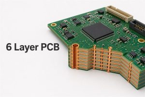
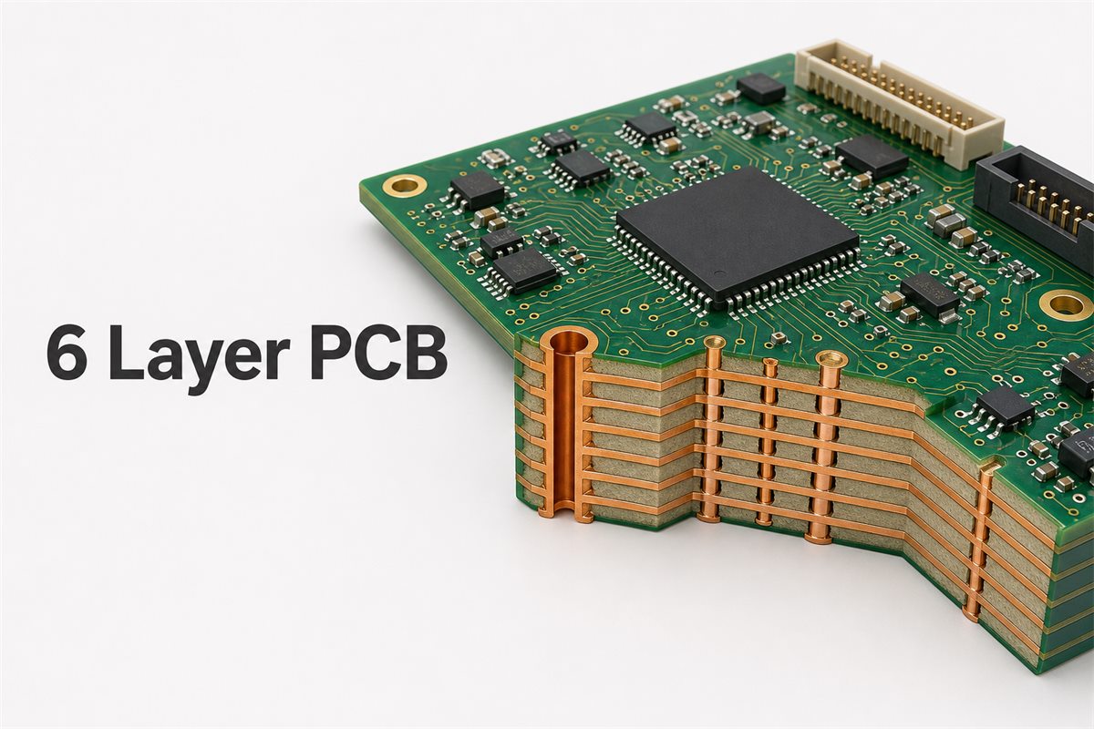
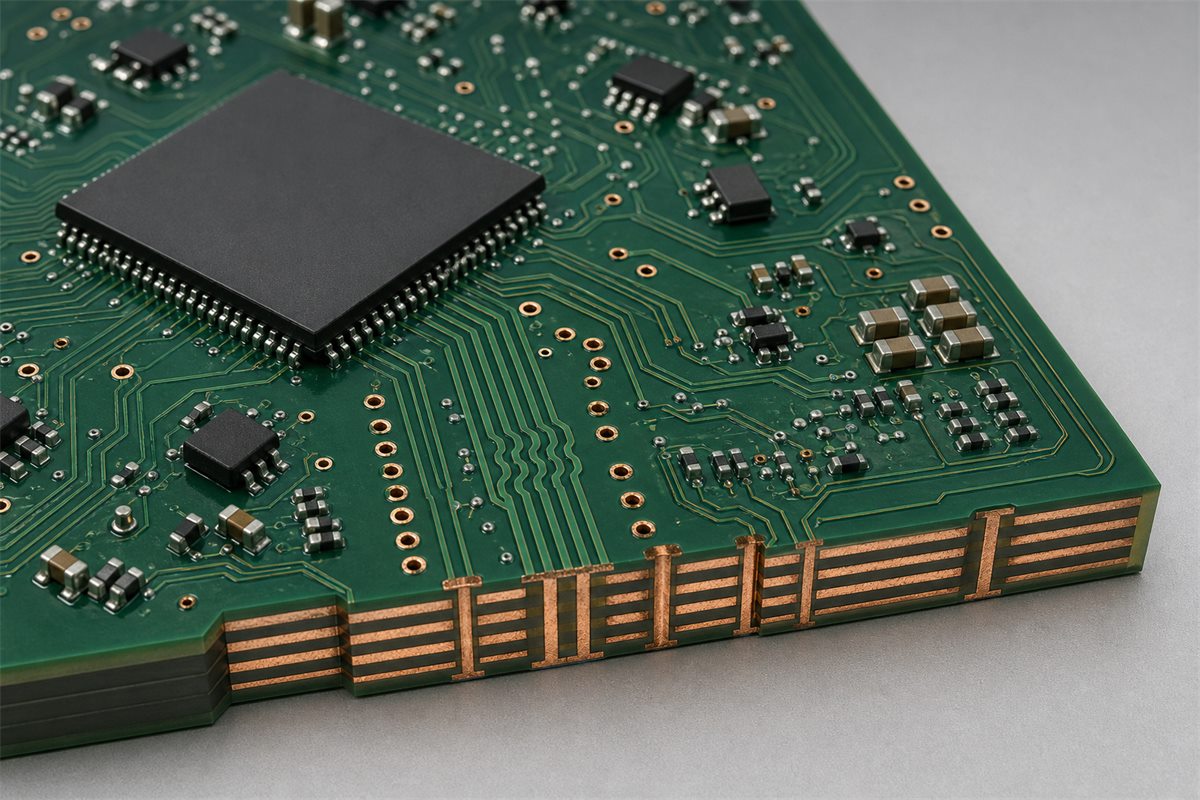
A 6 layer PCB has six conductive copper layers. They are separated by dielectric material. This construction is often selected when a four-layer board lacks routing space, reference planes, power distribution, or electromagnetic control, while an eight-layer construction would add unnecessary complexity.
Common assignments use the outer layers for components and signals, two inner layers as continuous reference planes, and the remaining inner layers for signals or power distribution. The exact arrangement depends on signal speed, return-current paths, component density, power rails, board thickness, and the fabricator’s available materials. When these constraints exceed what a four-layer stack can manage, moving to six layers provides four practical advantages:
- High-density routing: More internal routing capacity helps escape fine-pitch BGAs without forcing every connection onto the outer layers.
- Signal integrity: Closely coupled reference planes provide controlled return paths for high-speed and impedance-sensitive signals.
- Power distribution: Dedicated or shared plane layers can reduce loop area and organize multiple supply rails.
- EMI control: A deliberate layer order helps contain fields and reduces discontinuities caused by split or missing references.
Why Choose a 6 Layer PCB Instead of a 4 Layer or 8 Layer PCB?
Use six layers when four are insufficient and eight add no value. Layer count should follow routing, reference-plane, electrical, and layout constraints rather than a fixed rule.
| Decision Point | 4 Layer | 6 Layer | 8 Layer |
| Routing density | Moderate | High | Very high |
| Reference-plane options | Usually two internal planes | More flexible plane and signal allocation | More dedicated planes and routing pairs |
| High-speed routing | Suitable for controlled layouts with limited density | Good balance of routing space and return paths | Useful for dense buses, many rails, or stronger field containment |
| Manufacturing burden | Lower | Moderate | Higher material and process content |
A six-layer construction is not automatically cheaper than every eight-layer option. Standardized panel constructions, material utilization, via structure, copper weight, and factory loading can change the comparison. Request both stackup feasibility and a production quotation when the design can work on either layer count.
What Manufacturing Capabilities Should a 6 Layer PCB Manufacturer Provide?
A 6 layer PCB manufacturer must reproduce the approved stackup. Check the following six capabilities before releasing files or placing an order:
- Stackup engineering: Confirm cores, prepregs, finished thickness, copper distribution, resin needs, and impedance structures before artwork release.
- Registration control: Manage inner-layer alignment through tooling, imaging compensation, layup, lamination, and drilling.
- Hole reliability: Review finished hole size, drill diameter, copper thickness, aspect ratio, annular ring, and any blind or buried via sequence.
- Impedance verification: Calculate trace geometry from the production stackup and test representative coupons when specified.
- Electrical testing: Verify opens and shorts against the released netlist or approved manufacturing data.
- Documented inspection: Match inspection records and acceptance criteria to the product class and purchase order.
EBest Circuit offers FR-4, high-Tg, heavy-copper, HDI, high-speed, flexible, rigid-flex, and impedance-control products. Final limits must still be checked against the specific design through the verified PCB manufacturing capability and an engineering review.
What Materials, Copper Weights and Board Thicknesses Are Available?
Materials, copper weight, and thickness form one stackup system. Before quoting, the 6 layer PCB manufacturer should confirm how these choices affect impedance, drilling, copper balance, thermal performance, and lamination.
| Variable | Common Starting Choice | Engineering Check |
| Base material | FR-4 or high-Tg FR-4 | Confirm Tg, Td, CTE, Dk, Df, flammability requirement, and approved laminate family |
| Finished thickness | 1.0, 1.2, 1.6, or 2.0 mm may be requested | Confirm tolerance, connector fit, stiffness, impedance, and available core/prepreg construction |
| Copper weight | 1 oz is a common baseline | Separate starting copper from finished copper and review etching and hole-wall requirements |
| Surface finish | HASL, ENIG, OSP, immersion tin, or other qualified finish | Match shelf life, assembly process, pitch, bonding, contact use, and compliance needs |
Heavy copper requires wider spacing, suitable resin flow, and careful copper balance. High-speed materials require the actual laminate data used for impedance calculations. The final 6 layer PCB thickness must be checked against connector fit, stiffness, drilling, copper weight, and the available dielectric construction.
How Should a 6 Layer PCB Stackup Be Designed?
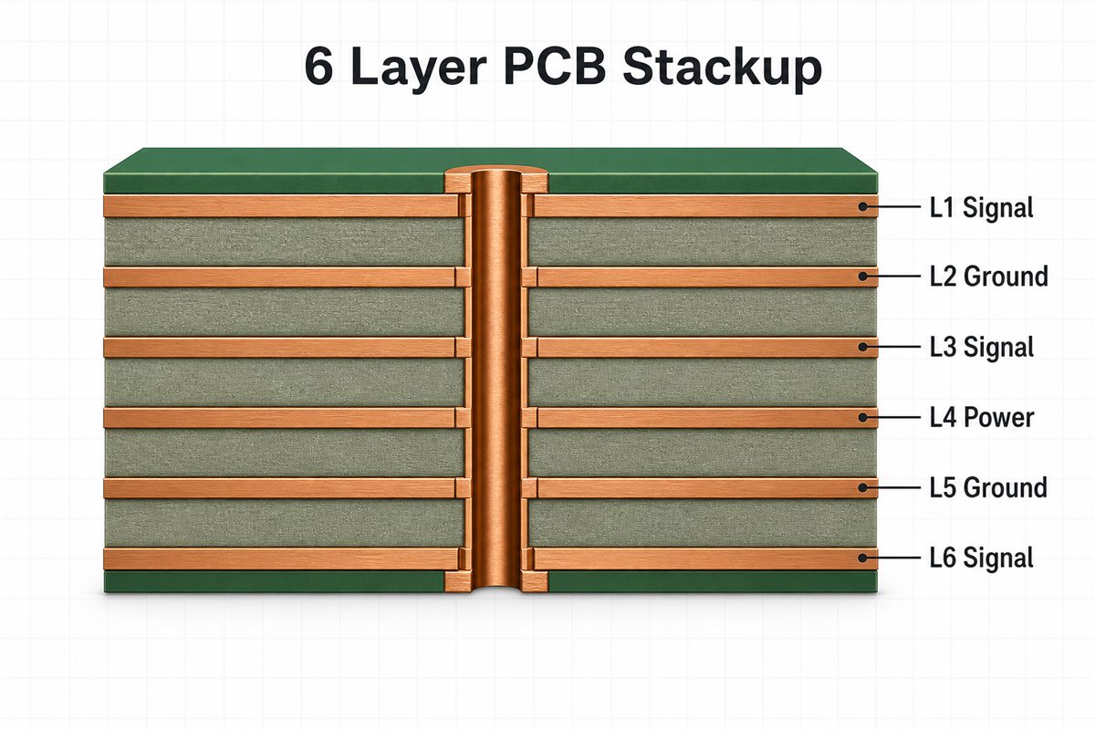
A good stackup uses continuous planes and symmetric construction. Critical signals should remain next to uninterrupted reference planes. Release final trace widths and dielectric thicknesses only after the 6 layer PCB manufacturer confirms its production materials.
The following balanced structure is a practical starting point for dense digital and mixed-signal designs. It gives both outer signal layers a nearby ground reference and reserves the two center layers for additional routing or power distribution.
| Layer | Typical Assignment | Reference and Design Purpose |
| L1 — Top | Components and critical signals | Route short high-speed connections over the solid L2 ground plane |
| L2 | Solid ground plane | Provides the primary return path and impedance reference for L1 and suitable L3 traces |
| L3 | Internal signals or power pours | Use L2 as the reference for controlled signals; keep power regions clear of critical return paths |
| L4 | Internal signals or power pours | Use L5 as the reference for controlled signals; coordinate spacing from L3 to limit broadside coupling |
| L5 | Solid ground plane | Provides the primary return path and impedance reference for L6 and suitable L4 traces |
| L6 — Bottom | Components and secondary signals | Route referenced signals over L5 and keep return paths continuous through layer changes |
This arrangement is not universal. Before routing, confirm these four points with the manufacturer:
- Reference continuity: Route critical nets over an uninterrupted ground reference and provide return transitions when changing layers.
- Layer symmetry: Balance dielectric and copper construction around the center to reduce bow and twist risk.
- Center-layer coupling: Set the L3-to-L4 spacing and routing directions to control broadside crosstalk.
- Production construction: Size controlled traces from the manufacturer’s released cores, prepregs, copper thicknesses, and impedance model.
What Design Files and DFM Checks Are Required Before 6 Layer PCB Fabrication?
Send the 6 layer PCB manufacturer one consistent data set. It must define geometry, drilling, stackup, materials, impedance, finish, profile, and acceptance requirements. Assembly orders also need component and placement data.
- Board image data: Supply Gerber X2 or ODB++ with a clear layer order and polarity.
- Drill data: Include plated and non-plated holes, slots, countersinks, and controlled-depth features where applicable.
- Fabrication drawing: State dimensions, tolerances, thickness, material, copper, finish, edge details, and special notes.
- Impedance table: Identify net class, target, tolerance, layer, reference, width, and differential spacing.
- Assembly package: Add BOM, centroid data, assembly drawings, approved substitutions, programming, and test instructions.
DFM should check annular rings, solder-mask clearances, copper-to-edge distance, drill-to-copper clearance, aspect ratio, via structures, copper balance, panelization, fiducials, tooling, and conflicts between drawings and data. Engineering questions should be closed in one approved revision set before the production clock starts.
How Does the 6 Layer PCB Manufacturing Process Work?
A 6 layer PCB manufacturer follows a controlled multilayer process. Production runs from data preparation and inner-layer imaging through lamination, hole metallization, outer-layer formation, finishing, and final testing. The following steps show what must be controlled before each operation advances.
- Step 1 — CAM and DFM preparation: Engineers compare Gerber or ODB++ data, drill files, the fabrication drawing, stackup, impedance requirements, and panel dimensions. CAM tools create the production panel, drill programs, imaging data, layer-scaling allowances, and test coupons after file conflicts are resolved.
- Step 2 — Inner-layer material preparation: Copper-clad cores are cut to panel size and cleaned so dry-film photoresist can bond uniformly. Material identity, copper weight, core thickness, surface condition, and orientation must match the approved stackup.
- Step 3 — Inner-layer imaging: The circuitry for the internal copper layers is transferred to the resist by laser direct imaging or another qualified exposure method. Developing removes the selected resist areas and leaves the copper pattern required for etching.
- Step 4 — Inner-layer etching and resist stripping: Unprotected copper is etched away to form the internal signal and plane patterns. The remaining resist is stripped, and conductor width, spacing, pad geometry, and unwanted residual copper are checked.
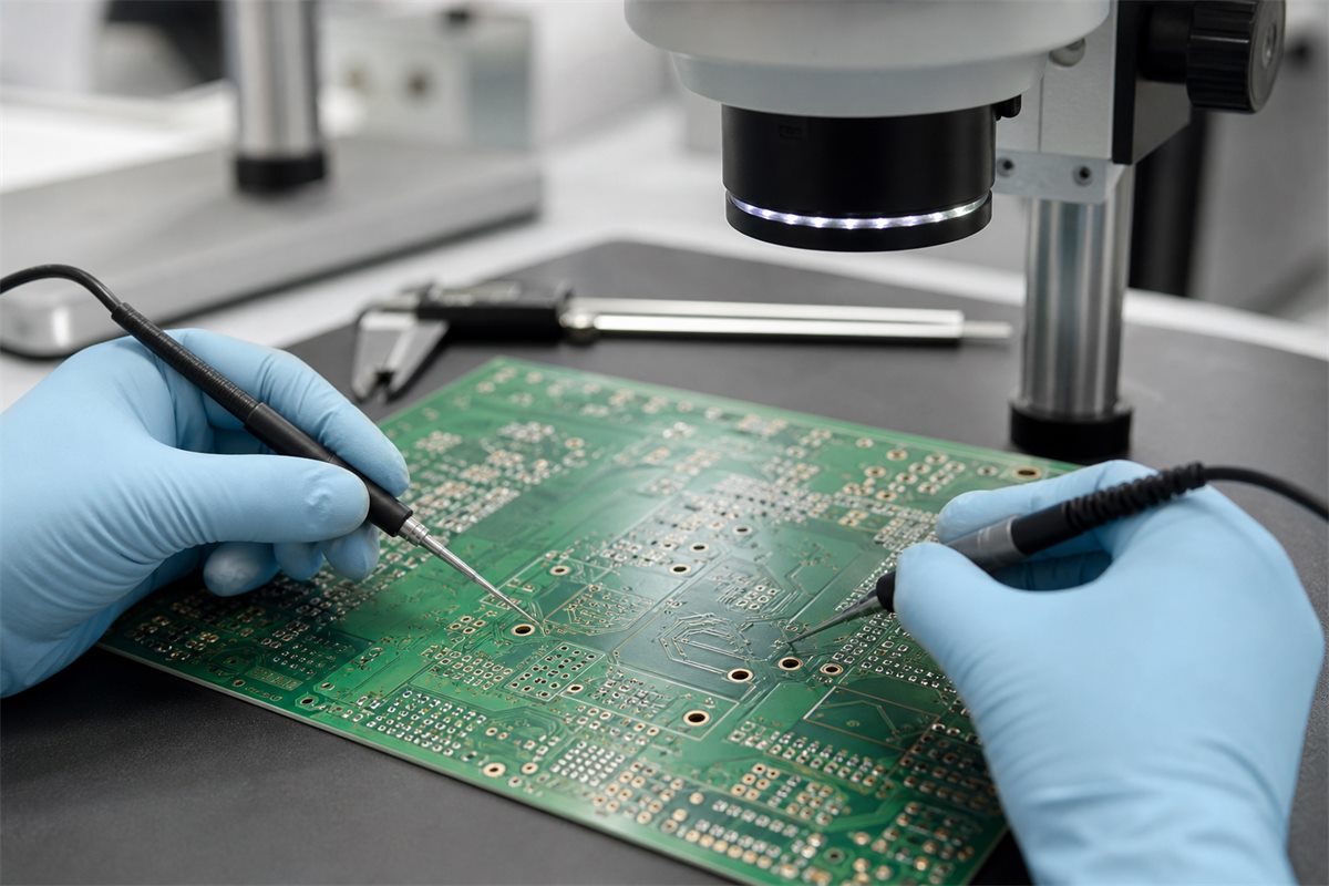
- Step 5 — Inner-layer AOI and registration review: Automated optical inspection compares each etched inner layer with the approved CAM image to find opens, shorts, nicks, spacing defects, or missing features. Registration targets are also checked because these circuits will become inaccessible after lamination.
- Step 6 — Bond treatment and six-layer layup: The inner copper surfaces receive a qualified bonding treatment, then cores, prepregs, and outer copper foils are stacked in the approved L1-to-L6 order. Tooling pins or another registration system align the layers, while prepreg type and resin content support dielectric thickness and copper filling.
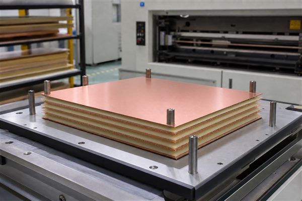
- Step 7 — Multilayer lamination: The six-layer book is pressed under a controlled temperature, pressure, vacuum, and time cycle. The prepreg resin flows, fills the copper topography, cures, and bonds the layers into one panel; the cycle must control thickness, voiding, registration, bow, and twist.
- Step 8 — X-ray registration and drilling: After lamination, X-ray targets or approved tooling references locate the buried inner-layer features before drilling. Mechanical or laser drilling produces plated holes, non-plated holes, slots, and any controlled-depth features according to the drill program.
- Step 9 — Desmear and hole-wall preparation: Drilling can leave resin smear over exposed inner-layer copper, so the holes are cleaned and micro-etched before metallization. This operation exposes sound copper and conditions the dielectric wall for a continuous conductive deposit.
- Step 10 — Electroless copper and panel plating: A thin electroless copper layer makes the hole walls conductive, followed by electrolytic copper plating to build the required hole-wall and surface copper. Plating distribution and copper thickness are controlled because insufficient or uneven deposition can weaken plated-through holes.
- Step 11 — Outer-layer imaging, pattern plating, and etching: The L1 and L6 circuit images are applied to the plated panel. Copper is built where required, an etch resist is added, unwanted outer copper is removed, and AOI checks the completed outer conductors against the CAM data.
- Step 12 — Solder mask, legend, and surface finish: Solder mask is applied, imaged, developed, and cured while pad openings and mask dams are inspected. The specified finish is then applied to exposed copper, followed by legend printing when required; finish choice and thickness must match the assembly and product requirements.
- Step 13 — Profiling, electrical test, and final release: Routing, scoring, or another approved method forms the final board outline and any internal cutouts. The finished boards undergo netlist electrical testing, dimensional and visual inspection, and any specified impedance, microsection, cleanliness, or documentation checks before packing and release.
What Specialized 6 Layer PCB Types Can We Manufacture?
Specialized six-layer boards require a matching process route. Six-layer construction can support rigid, heavy-copper, HDI, high-speed, flexible, and rigid-flex products. These options are not interchangeable add-ons.
- Heavy copper: Suits higher-current and thermal demands but changes spacing, etching, resin filling, and finished-thickness planning.
- HDI: Uses microvias, sequential lamination, finer geometry, or via-in-pad structures when BGA escape density requires them.
- High-speed and RF: Requires laminate control, loss planning, reference continuity, and production impedance correlation.
- Flexible and rigid-flex: Requires bend-zone rules, coverlay, stiffeners, flex material control, and transition design. Review the verified flex PCB manufacturer requirements before release.
Send the complete mechanical and electrical requirements for feasibility review. A six-layer rigid-flex board, a six-layer HDI board, and a heavy-copper six-layer board follow different material and process controls even though the layer count is the same.
What 6 Layer PCB Manufacturing and Assembly Services Can We Provide?
Manufacturing and assembly stay coordinated from prototype to volume. Customers can place bare-board fabrication, component sourcing, and assembly under one controlled project revision.
Manufacturing starts with the approved board data and ends with inspected bare boards ready for assembly. The production scope should define the following requirements:
- Stackup and material control: Build the six-layer construction from the approved core, prepreg, laminate grade, copper weight, finished thickness, and surface-finish requirements.
- Impedance-controlled fabrication: Review controlled nets, target impedance, tolerance, reference layers, trace geometry, and the production stackup before releasing the board.
- Drilling and plating: Manufacture through holes and any specified blind or buried vias according to finished-hole size, aspect ratio, annular-ring, and copper-plating requirements.
- Bare-board inspection: Apply the agreed electrical test and dimensional inspection requirements before boards move to assembly or shipment.
- Prototype and volume supply: Support initial board quantities and later mass production while keeping the approved fabrication revision under change control.
Assembly service adds parts procurement and component installation to the manufactured board. The order review should separate standard assembly work from project-specific operations:
- Component sourcing: Purchase parts against the approved BOM and identify manufacturer part numbers, approved alternatives, do-not-substitute items, and customer-supplied components.
- Assembly preparation: Check the BOM, pick-and-place file, assembly drawing, reference designators, polarity, package data, keep-out areas, and component-height restrictions for consistency.
- Prototype assembly: Use the first build to confirm component fit, placement data, assembly notes, test access, and any programming requirements before volume release.
- Volume assembly: Freeze the approved PCB revision, BOM, placement files, and substitution rules after sample approval to prevent mixed board or component revisions.
- Project-specific operations: Programming, functional testing, conformal coating, special cleaning, traceability records, and detailed inspection reports require feasibility and acceptance-criteria confirmation during quotation.
To price manufacturing and assembly together, submit one complete and revision-matched data package. This allows material, component, tooling, testing, and delivery requirements to be reviewed at the same time:
- PCB production data: Gerber or ODB++, NC drill files, board drawing, stackup, impedance table, panel requirements, and finished-board specifications.
- Component data: BOM with manufacturer part numbers, quantities, approved alternates, do-not-substitute parts, and a list of consigned components.
- Assembly data: Pick-and-place file, assembly drawing, polarity and orientation notes, reference designators, and any keep-out or height restrictions.
- Order quantities: Prototype quantity, expected production quantity, delivery schedule, and whether extra boards or components are allowed for process setup.
- Acceptance requirements: Required inspection records, electrical or functional tests, programming files, test fixtures, packaging, cleaning, coating, and traceability needs.
How Is Quality Controlled During 6 Layer PCB Fabrication and Assembly?
Quality must be verified at each production gate. This prevents hidden inner-layer, plated-hole, electrical, or assembly defects from reaching final inspection. Each gate should have a defined requirement, inspection method, acceptance limit, and release record.
| Quality gate | What is controlled | Evidence to define or request |
| Incoming materials | Laminate type, copper weight, component identity, quantity, packaging condition, and specified compliance | Material identification, receiving record, lot information, or supplier documentation required by the order |
| Inner-layer circuits | Trace pattern, shorts, opens, clearances, copper defects, and layer registration before lamination | Inner-layer inspection status and disposition of detected defects |
| Layup and lamination | Layer order, core and prepreg selection, copper balance, registration, resin flow, and finished construction | Approved stackup, traveler records, thickness check, and cross-section requirements when specified |
| Drilling and hole preparation | Drill size, hole position, smear removal, via structure, annular ring, and wall condition | Drill data verification, registration results, and microsection criteria for plated holes when required |
| Hole metallization and plating | Copper continuity, plated-hole integrity, surface copper build, and finished-hole size | Plating records, finished-hole inspection, and coupon or microsection results defined by the purchase specification |
| Outer layers and solder mask | Finished trace geometry, pads, solder-mask registration, legend readability, and surface-finish condition | Final visual and dimensional inspection results against released artwork and drawings |
| Electrical and impedance verification | Opens, shorts, netlist continuity, and controlled-impedance structures | Electrical-test status and impedance coupon data when coupon testing is included in the order |
| Assembly release | Component identity, orientation, solder-joint condition, workmanship, programming, and functional requirements | Specify the required inspection or test record; AOI, X-ray, programming, and functional testing remain order-dependent |
| Final shipment release | Board dimensions, quantity, revision, packaging, labeling, documentation, and nonconformance closure | Final inspection record, certificate of conformance, test report, or traceability record when contractually required |
EBest Circuit lists ISO 9001:2015, ISO 13485:2016, IATF 16949, AS9100D, UL, RoHS, and REACH among its quality and compliance credentials. For regulated or high-reliability work, request the current certificate, site scope, product applicability, revision, and required order records before approval.
What Factors Affect 6 Layer PCB Price and Lead Time?
The full process route determines price and lead time. Layer count alone is not enough. A quote becomes reliable when it is based on released data and a confirmed stackup.
- Panel utilization: Board dimensions, rails, coupons, routing gaps, and quantity determine material yield.
- Material system: High-Tg, low-loss, flex, rigid-flex, or uncommon laminate choices affect availability and processing.
- Copper and geometry: Heavy copper, fine lines, tight spacing, small annular rings, and dense drilling increase process difficulty.
- Via structure: Blind, buried, microvia, stacked, filled, or capped vias can add lamination and plating operations.
- Testing scope: Impedance coupons, electrical test, microsection, ionic cleanliness, X-ray, programming, and functional test require time and resources.
- Assembly supply chain: BOM availability, approved substitutions, component packaging, and fixture readiness often control the PCBA schedule.
Compare quotations using the same revision, quantity, material, copper, finish, test scope, quality documentation, shipping terms, and schedule start condition. A low headline price is not comparable if it excludes tooling, testing, controlled impedance, or assembly requirements.
Custom 6 Layer PCB Manufacturing and Assembly Case Study
A credible case study shows decisions and verifiable outputs. This representative industrial-control project explains what must be resolved before a custom six-layer board reaches production.
Project Background: The design needed more routing space than a four-layer board could provide. It also required continuous reference planes, multiple power rails, controlled-impedance signals, and an assembled prototype that would fit an existing enclosure.
Project Requirements: The release package contained Gerber and NC drill data, a preliminary stackup, impedance net classes, a BOM, pick-and-place data, assembly drawings, mechanical limits, programming requirements, and functional-test criteria. The main risks were inconsistent layer naming, incomplete impedance references, component substitutions, and uncontrolled changes between fabrication and assembly files.
Engineering Review: The board data was checked against the proposed layer order and drill pairs. Reference-plane continuity, BGA escape routing, copper distribution, panel requirements, dielectric availability, and manufacturable impedance geometry were reviewed together. BOM alternatives, polarity notes, package data, and test access were then resolved before release.
Manufacturing and Assembly Control: The approved stackup and artwork revision became the manufacturing baseline. The BOM, placement file, assembly drawing, and programming package were tied to the same revision so that a board change could not enter assembly without review.
Customer-Verifiable Output: The deliverable package can include the approved stackup, resolved engineering questions, released fabrication data, assembled samples, and electrical-test status. It can also include specified inspection records and a change log. These records let the customer compare the prototype and later production build against the same approved baseline.
Why Choose EBest Circuit as Your 6 Layer PCB Manufacturer in China?
One accountable source reduces handoff risk. Customers can coordinate design support, six-layer PCB production, component sourcing, and assembly through EBest Circuit, reducing the time and risk created by separate suppliers.
- Fewer supplier handoffs: One project team can coordinate the stackup, bare-board data, BOM, placement files, and assembly requirements, reducing duplicated questions and conflicting revisions.
- Lower design-release risk: Material availability, layer order, copper distribution, reference planes, drilling, impedance, and assembly data can be reviewed before production consumes material.
- More predictable repeat orders: The approved manufacturing package and change history provide a controlled baseline for later builds instead of relying on undocumented production assumptions.
- Simpler component coordination: Approved alternatives, customer-supplied parts, do-not-substitute items, and shortage decisions can be resolved within the same order as PCB production.
- Quality evidence matched to your risk: Customers can specify electrical tests, impedance records, inspection reports, traceability, and certificates that their product or quality system actually requires.
- Support from prototype to volume: PCB design, prototyping, mass production, component sourcing, and assembly services allow the same technical decisions to carry forward as quantities increase.
For a custom 6 layer PCB manufacturer quotation, send the released data package and identify the requirements that affect stackup, impedance, reliability, assembly, testing, quality records, and delivery.
FAQs About 6 Layer PCB Manufacturing
Q1: Can edge plating or castellated holes be added to a 6 layer PCB?
A1: Yes, when the board outline and plating requirements are designed for the selected feature. Define plated edges or castellations in the fabrication drawing and confirm minimum feature size, routing method, and finished-edge acceptance criteria.
Q2: Can press-fit connectors be used on a 6 layer PCB?
A2: Yes, but finished-hole geometry and plating must match the connector specification. Provide the connector drawing, compliant-pin range, hole tolerance, copper requirement, board thickness, and insertion-force constraints for review.
Q3: Should unused vias be tented, plugged, filled, or capped?
A3: Select the treatment from the via location and assembly risk. BGA escape vias, via-in-pad structures, exposed test vias, and holes near solderable pads may require different treatments to control solder loss, contamination, or surface flatness.
Q4: How should tooling holes and fiducials be specified for assembly?
A4: Define them at both board and panel level when the assembly process requires them. Their size, location, clearance, and relationship to breakaway rails should be coordinated with placement, inspection, and depaneling needs.
Q5: Can controlled-depth routing or cavities be used in a 6 layer PCB?
A5: These features are possible only after mechanical and stackup review. The drawing should define depth, tolerance, remaining dielectric or copper, corner radius, and the relationship to internal conductors.
Q6: What information is needed for selective conformal coating?
A6: Provide a coating drawing with coated and keep-out areas clearly marked. Identify connectors, test points, switches, heat sinks, grounding contacts, coating material, thickness requirement, masking method, and inspection criteria.
Q7: How should firmware and programming files be controlled?
A7: Treat firmware as a released production item with its own revision. Specify the device, file name, checksum or version, programming interface, security requirements, verification method, and labeling rule.
Q8: What packaging should be specified for assembled six-layer boards?
A8: Packaging should match moisture, ESD, mechanical, and cleanliness risks. Define ESD protection, moisture barrier requirements, desiccant, humidity indication, tray or reel orientation, cushioning, labels, and shipment quantity per package.
Q9: Can serial numbers, date codes, or lot codes be added?
A9: Yes, when the marking content, format, location, and data source are defined. Confirm whether markings are human-readable, machine-readable, permanent, linked to test records, or restricted by available board space.
Q10: How are approved component substitutions documented?
A10: Every substitute should be approved against defined electrical, mechanical, and lifecycle criteria. Record the alternate manufacturer part number, affected reference designators, approval authority, applicable quantity, and whether the change is temporary or permanent.
Conclusion
One approved production baseline reduces preventable variation. A reliable six-layer build keeps stackup, materials, impedance, drilling, plating, component data, inspection, and assembly under revision control. Coordinating these decisions with one manufacturing partner can reduce file conflicts, repeated engineering questions, component delays, and uncontrolled changes between prototype and volume production.
Send your Gerber/ODB++, NC drill files, stackup, BOM, and quantity, together with assembly drawings, programming files, test requirements, and required quality records, to sales@bestpcbs.com. EBest Circuit will review the manufacturing and assembly scope and prepare a project-specific quotation.