PCB manufacturing PCB manufacturing
Home > Blog

10 Layer PCB Fabrication

How Do You Make a PCB? Design, Fabrication and Assembly Steps
Thursday, July 9th, 2026

To make a PCB, you first turn a circuit idea into a schematic, convert the schematic into a PCB layout, export manufacturing files, fabricate the bare board, assemble components, inspect solder joints, and test the finished assembly. For a reliable result, the process should be treated as an engineering workflow, not only as a drawing or etching task.
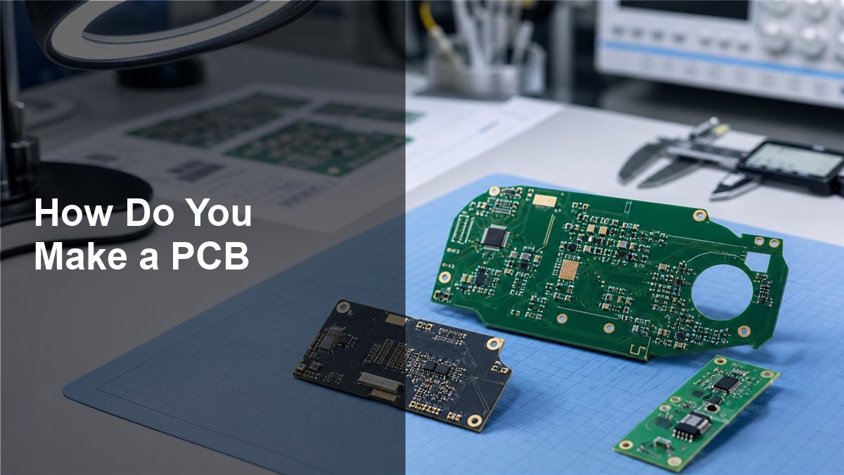
How Do You Make a PCB hero image with printed circuit boards on an engineering workbench
A PCB starts as a circuit design, but quality depends on layout, fabrication, assembly, and testing decisions.

This guide explains how a PCB is made from a practical design and manufacturing perspective. It covers the steps a designer, engineer, buyer, or sourcing team should understand before sending files to a PCB manufacturer or PCBA supplier.

Start With the Circuit Requirement

A PCB project should start with the circuit function, operating environment, component needs, and production goal.

Before drawing the board, define what the circuit must do, how much current it carries, what voltage levels are involved, which signals are sensitive, and whether the board must fit inside a mechanical enclosure. Also decide whether the PCB is only for a prototype, a small engineering build, or a product that may later move into mass production.

This early definition affects material choice, board size, layer count, trace width, connector position, test points, assembly method, and cost. A simple sensor board may only need two layers, while a compact control board with high-speed signals may need more layers, controlled impedance, tighter spacing, and stronger documentation.

Create the Schematic

The schematic is the electrical map that shows components, nets, power rails, connectors, and circuit relationships.

In the schematic stage, select real components, check datasheets, assign symbols, define power input, add protection where needed, and confirm that every signal has a clear source and destination. Use meaningful net names for power, ground, communication buses, and important signals so the layout and review process are easier.

Good schematic work also includes checking component availability, package options, voltage ratings, current ratings, and thermal limits. If a part has several package choices, confirm which footprint will be used before the PCB layout begins.

Convert the Schematic Into a PCB Layout

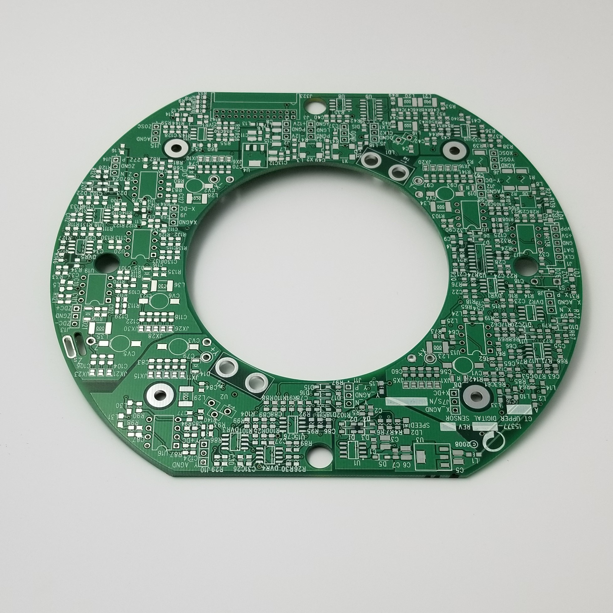
The PCB layout turns the electrical schematic into physical copper traces, pads, vias, planes, and board outlines.

During layout, place connectors and mechanical parts first, then position ICs, power components, decoupling capacitors, crystals, sensors, and critical signal paths. Keep related components close together, route power and ground carefully, and leave enough space for assembly, inspection, and rework.
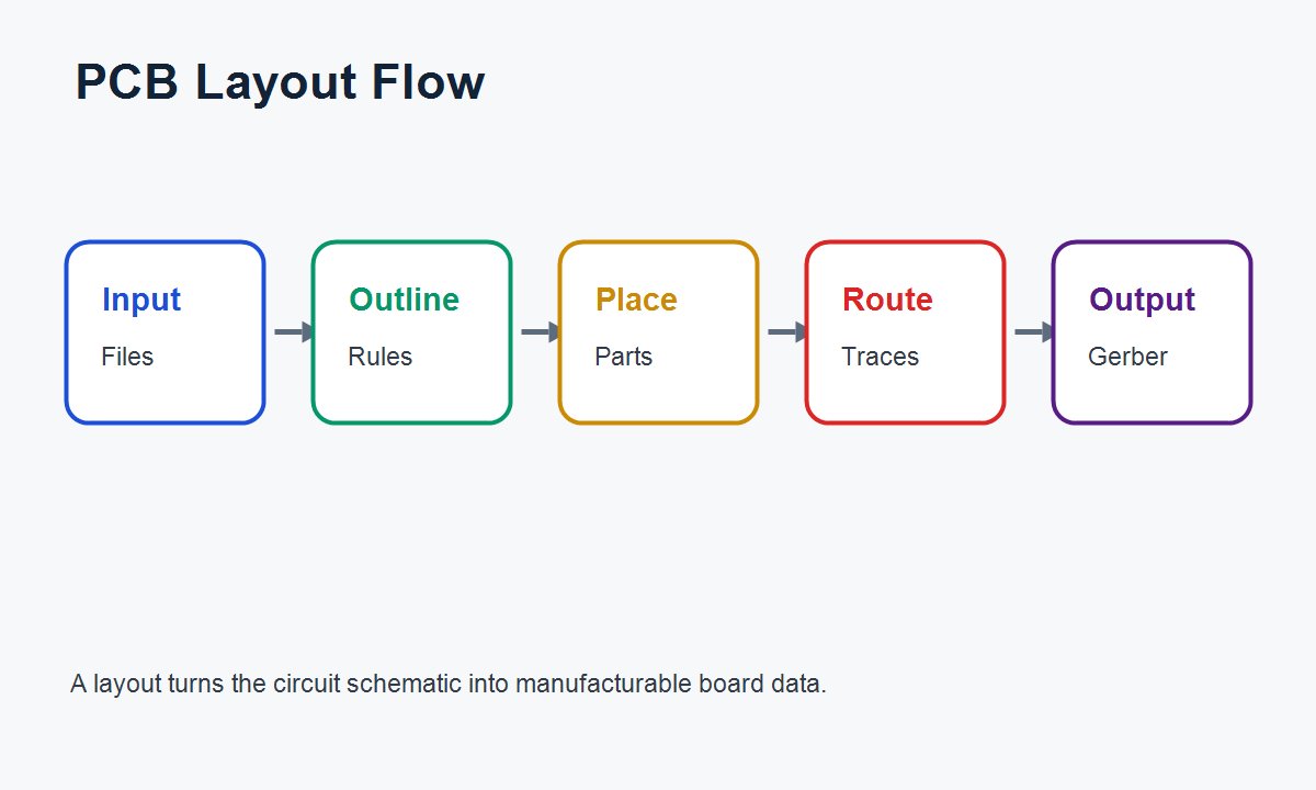
PCB design workflow from schematic to layout and Gerber file preparation
The layout stage converts the schematic into board geometry, copper routing, drill data, and manufacturing outputs.

Design rules should match the PCB manufacturer capability. Check minimum trace width, minimum spacing, drill size, annular ring, solder mask clearance, copper thickness, via type, and board thickness before finalizing the layout. Using rules that are too aggressive can increase cost or create manufacturing risk.

Prepare PCB Manufacturing Files

Manufacturing files tell the factory exactly how to build the bare PCB.

The most common file package includes Gerber files, drill files, board outline, stackup notes, copper thickness, solder mask color, silkscreen requirements, surface finish, impedance notes if needed, and fabrication drawings for controlled dimensions or tolerances. For assembly, add a BOM, pick-and-place file, assembly drawing, polarity notes, and special handling requirements.

File or Note What It Controls Why It Matters
Gerber files Copper, solder mask, silkscreen, paste, and board outline layers Defines the physical board pattern used for fabrication
Drill files Plated and non-plated holes Controls vias, mounting holes, and through-hole component holes
Stackup notes Layer order, dielectric thickness, copper weight, impedance needs Important for multilayer boards and signal performance
BOM Component part numbers, quantities, values, and packages Required for sourcing and PCBA assembly
Pick-and-place file Component coordinates and rotation Helps automated assembly place parts accurately

Run DFM Checks Before Fabrication

DFM checks help catch layout and file problems before the board enters production.

Useful checks include missing board outline, mismatched drill files, insufficient solder mask clearance, copper too close to the edge, unreadable silkscreen, tiny annular rings, incorrect footprints, polarity ambiguity, and spacing that does not match the factory capability. These issues are easier to fix before ordering boards than after fabrication.

For assembled boards, also check part availability, alternate parts, component orientation, fiducials, panelization, stencil openings, thermal pads, and test access. Small layout changes can improve assembly yield and reduce manual rework.

Fabricate the Bare PCB

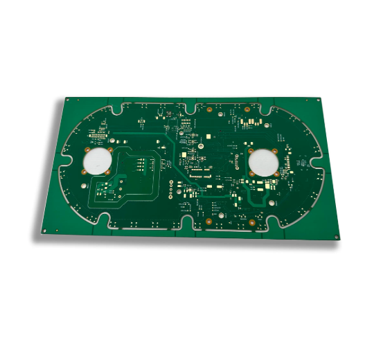
PCB fabrication builds the physical board by processing laminate, copper layers, drilled holes, plating, solder mask, silkscreen, and surface finish.

A simplified fabrication flow includes material preparation, inner layer imaging for multilayer boards, lamination, drilling, copper plating, outer layer imaging, etching, solder mask application, silkscreen printing, surface finish, profiling, electrical test, and final inspection. Exact steps depend on layer count, material, copper thickness, via structure, and surface finish.
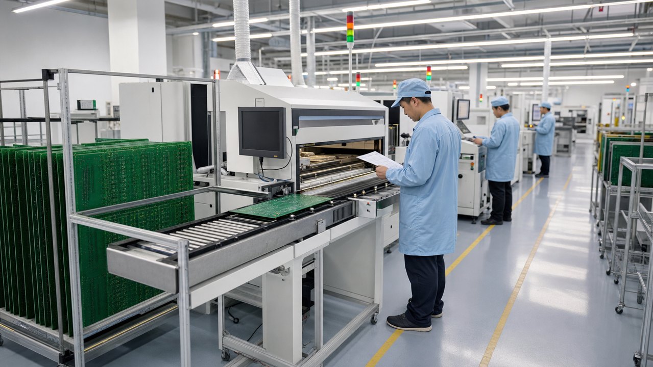
PCB fabrication production line for making printed circuit boards
PCB fabrication turns the digital manufacturing files into physical copper layers, plated holes, solder mask, and finished boards.

Common surface finishes include HASL, lead-free HASL, ENIG, immersion silver, immersion tin, OSP, and others. The right choice depends on component pitch, shelf life, solderability, cost, and application requirements. Fine-pitch parts, BGAs, or high-reliability assemblies often need more careful surface finish selection.

Assemble the Components

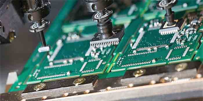
PCB assembly places and solders components onto the fabricated board.

For SMT assembly, solder paste is usually printed through a stencil, components are placed by machine, and the board passes through controlled reflow. Through-hole parts may be hand soldered, wave soldered, or selective soldered depending on volume, component type, and board design.

Assembly quality depends on footprint accuracy, stencil design, solder paste volume, component orientation, reflow profile, thermal balance, and inspection. Dense boards, BGAs, QFNs, fine-pitch ICs, and mixed technology boards need stronger process control than simple prototype boards.

Inspect and Test the PCB

Inspection and testing confirm that the board was built correctly before it is shipped or used in a product.

Bare boards may go through electrical testing, visual inspection, dimensional checks, and solder mask inspection. Assembled boards may use AOI, X-ray for hidden solder joints, in-circuit test, functional test, continuity checks, and first article inspection depending on the application.
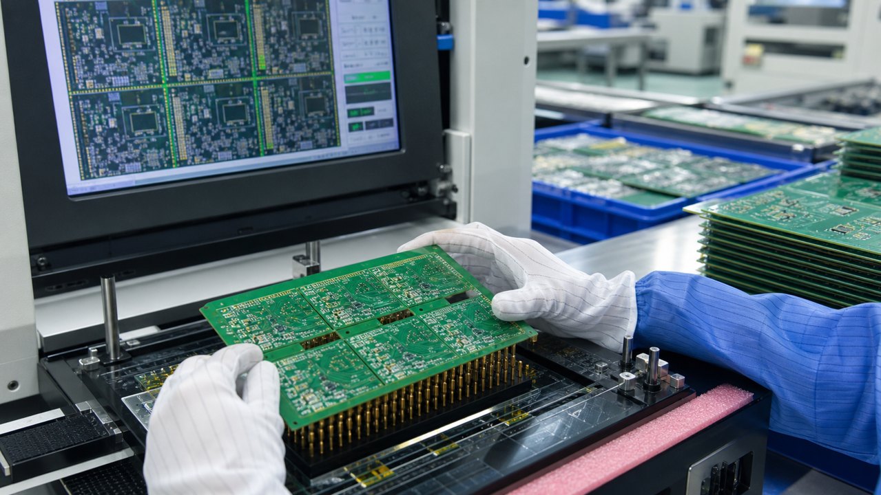
PCB quality inspection after fabrication and assembly
Inspection and testing catch fabrication defects, assembly problems, solder issues, and documentation mismatches.

Do not rely only on whether the board powers on. A board can appear functional but still have weak solder joints, marginal clearances, missing components, incorrect substitutions, or process risks that affect later reliability.

Prototype Before Mass Production

A prototype helps confirm the design, files, components, assembly process, and test plan before larger production.

Use the prototype stage to validate the schematic, layout, mechanical fit, connector position, thermal behavior, signal quality, firmware access, and production documentation. Record any manual rework because it may reveal footprint errors, missing test points, incorrect polarity markings, or assembly access problems.

If the prototype passes, update the design files and production notes before scaling. The most useful prototype is not only a working board, but a learning step that improves repeat production.

Common Mistakes When Making a PCB

Many PCB problems come from weak file preparation, unclear requirements, or layout choices that ignore manufacturing and assembly limits.

Mistake Possible Result Prevention
Using unverified footprints Parts do not fit or solder correctly Compare footprints with datasheets and actual packages
No clear board outline Factory must ask for clarification or may route incorrectly Include a defined mechanical layer and fabrication drawing
Ignoring manufacturer design rules Higher cost, delays, or fabrication risk Set trace, spacing, drill, annular ring, and mask rules early
Missing polarity markings Assembly errors or damaged components Make diode, LED, capacitor, IC, and connector orientation clear
No test points Difficult debugging and production testing Add accessible points for power, ground, programming, and critical signals

What Should You Send to a PCB Manufacturer?

A manufacturer needs clear files, specifications, and production requirements to quote and build the board correctly.

For bare PCB fabrication, send Gerber files, drill files, board dimensions, layer count, material preference, copper thickness, board thickness, solder mask color, silkscreen color, surface finish, quantity, and special requirements. For PCBA, also include the BOM, pick-and-place file, assembly drawing, component sourcing notes, firmware or programming needs, and test requirements.

If you are unsure whether the files are complete, ask for an engineering review before production. A file check can catch missing drill data, unclear stackup, unsuitable footprints, and assembly concerns before they become real cost or schedule problems.

FAQ About How Do You Make a PCB

How do you make a PCB step by step?

You make a PCB by defining the circuit, drawing a schematic, creating the PCB layout, exporting Gerber and drill files, running DFM checks, fabricating the bare board, assembling components, inspecting solder joints, and testing the finished board.

Can I make a PCB at home?

You can make simple single-sided boards at home using hobby methods, but home PCB making is limited in accuracy, plating, solder mask, vias, and repeatability. For reliable prototypes or production boards, professional fabrication is usually safer.

What files are needed to make a PCB?

For bare PCB fabrication, the usual files are Gerber files, drill files, board outline, and fabrication notes. For assembly, also provide a BOM, pick-and-place file, assembly drawing, polarity notes, and test requirements.

How long does it take to make a PCB?

Lead time depends on layer count, material, surface finish, quantity, complexity, assembly needs, and supplier capacity. Simple prototypes can be faster than multilayer, impedance-controlled, high-density, or assembled boards. Confirm timing with the manufacturer before ordering.

What is the difference between PCB fabrication and PCB assembly?

PCB fabrication makes the bare printed circuit board with copper, holes, solder mask, silkscreen, and surface finish. PCB assembly places and solders components onto that bare board, then inspects and tests the assembled product.

Do I need a schematic before making a PCB?

Yes, a schematic is strongly recommended because it defines the circuit and net relationships. You can sometimes copy a simple board layout directly, but a schematic makes checking, debugging, and future revisions much safer.

What software is used to make a PCB?

Common PCB design tools include KiCad, Altium Designer, Eagle, Fusion 360 electronics tools, OrCAD, and other EDA platforms. The right tool depends on design complexity, team workflow, file requirements, and budget.

Why is DFM important when making a PCB?

DFM checks confirm that the layout matches manufacturing and assembly limits. They help prevent delays, extra cost, soldering problems, missing files, weak clearances, and design choices that a factory cannot build reliably.

Can a PCB manufacturer help check my files?

Many PCB manufacturers can review Gerber files, drill data, stackup notes, BOMs, and assembly files before production. The review does not replace design responsibility, but it can catch practical fabrication and assembly issues.

What is the most common reason a first PCB fails?

Common reasons include wrong footprints, reversed polarized components, missing pull-up or pull-down resistors, poor power layout, unclear connectors, inadequate test points, and design rules that do not match the manufacturer capability.

Final Thoughts

Making a PCB is a connected process: circuit definition, schematic, layout, manufacturing files, fabrication, assembly, inspection, and testing all affect the final result. A clean layout is not enough if the files are incomplete, the footprints are wrong, or the assembly requirements are unclear.

If you are preparing a PCB or PCBA project, BestPCBs can support prototype development, PCB fabrication, PCB assembly, OEM/ODM manufacturing, and engineering file review. Send your Gerber files, BOM, drawings, quantity, and special requirements to sales@bestpcbs.com for technical support and a quote.

You may also like

10 Layer PCB Design & Manufacturer, Direct From Factory
Wednesday, November 12th, 2025

What is 10 layer PCB? Let’s discover its thickness, stackup, design spec and guide, production process, cost, difference between 8 layer PCB via this blog.

Are you troubled with these problems?

  • Is controlling the alignment accuracy between layers in high-layer PCBs difficult, leading to unstable signal transmission?
  • Are thermal management challenges in 10-layer boards affecting product performance and lifespan?
  • Long lead times for small-batch, high-variety orders impacting project schedules?

As a 10 layer PCB manufacturer, EBest Circuit (Best Technology) can provide you service and solution:

  • Innovative interlayer alignment technology ensuring zero signal loss in 10-layer board signal transmission;
  • Intelligent thermal management solutions improving product heat dissipation efficiency by over 30%;
  • A rapid-response production system enabling 7-day express delivery for small-batch orders.

Welcome to contact us if you have any inquiry for 10 layer PCB design and manufacturing: sales@bestpcbs.com.

What Is 10 Layer PCB?

A 10 layer PCB is a multilayer printed circuit board composed of ten layers of conductive copper foil and insulating material, stacked alternately. Its core advantage lies in achieving a more complex and high-density circuit layout within a limited space through this multilayer structure.

Compared to ordinary 2-layer or 4-layer boards, 10-layer PCBs offer superior performance in signal transmission speed, power distribution, and electromagnetic compatibility (EMC), effectively suppressing electromagnetic interference and improving system stability. They are commonly found in high-end communication equipment, servers, smartphones, and other applications with high performance and signal integrity requirements.

What Is 10 Layer PCB?

How Thick Is a 10 Layer PCB?

The thickness of a 10-layer PCB typically ranges from 0.8mm to 3.2mm, with 1.6mm being the most common standard thickness (accounting for approximately 60% of industry applications). Specific values ​​are dynamically adjusted based on substrate type (e.g., FR-4, high-frequency materials), copper foil thickness (primarily 0.5oz for the inner layer and 1oz for the outer layer), and impedance control requirements. The tolerance range is generally ±10% of the nominal thickness. For example, the actual thickness of a 1.6mm board needs to be controlled between 1.44-1.76mm, while ultra-thin designs (0.8mm) are mostly used in mobile devices, and thicker boards (2.0mm and above) are suitable for high-power applications.

How Thick Is a 10 Layer PCB?

10 Layer PCB Stackup Example

Layer NumberLayer TypeDescription
1Top Signal LayerLow-speed signals, component placement
2Ground Layer (GND)Provides return path for top layer and layer 3
3High-Speed Signal LayerCritical signals (e.g., clocks, differential pairs)
4High-Speed Signal LayerOrthogonal routing to layer 3 to reduce crosstalk
5Power Layer (PWR)Primary power distribution
6Ground Layer (GND)Forms tightly coupled power-ground plane with layer 5
7High-Speed Signal LayerSame as layers 3 and 4, embedded between planes
8High-Speed Signal LayerOrthogonal routing to layer 7
9Ground Layer (GND)Provides return path for layer 8 and bottom layer
10Bottom Signal LayerLow-speed signals, component placement

Difference Between 8 Layer vs 10 Layer PCB

1. Layer Count and Structure

  • 8 Layer PCB: 4 signal layers + 2 power/ground planes + 2 hybrid layers. Typical stackup alternates signal-power-ground-signal for balanced coupling.
  • 10 Layer PCB: 6 signal layers + 3 power/ground planes + 1 shielding layer. Additional layers enable finer signal isolation and reference plane segmentation, e.g., high-speed layers embedded between planes.

2. Routing Capability and Density

  • 8 Layer PCB: Medium complexity routing channels support BGA pitches ≥0.8mm, suitable for PCIe 3.0/4.0 interfaces.
  • 10 Layer PCB: High-density routing supports BGA pitches ≤0.5mm, accommodating PCIe 5.0/6.0, DDR5, and other high-bandwidth interfaces with 20-30% more routing channels.

3. Signal Integrity (SI) and Electromagnetic Compatibility (EMC)

  • 8 Layer PCB: Mid-frequency (≤5GHz) signals achieve low crosstalk via symmetric power-ground planes. EMI radiation meets standard limits.
  • 10 Layer PCB: High-frequency (>10GHz) signals benefit from multi-layer reference planes, reducing crosstalk by 15-20dB and improving mixed-signal isolation. EMC immunity enhances.

4. Power Integrity (PI) and Thermal Management

  • 8 Layer PCB: Dual power-ground planes support ≤10A current. Thermal management relies on inner copper foils, limiting temperature rise to ≤15°C.
  • 10 Layer PCB: Triple-plane design reduces power impedance (≤1mΩ) and supports >15A current. Copper thickness accumulation improves thermal efficiency by 20%, reducing temperature rise to ≤10°C.

5. Cost and Manufacturing Lead Time

  • 8 Layer PCB: Lower material costs by 20-30%, shorter lead time by 1-2 weeks, yield rate ≥95%. Ideal for mass production.
  • 10 Layer PCB: Higher alignment complexity reduces yield to 90-93%, increases cost by 30-50%, and extends lead time by 2-3 weeks. Suitable for high-requirement projects.

6. Reliability and Mechanical Strength

  • 8 Layer PCB: Sufficient durability for conventional industrial/consumer environments. Bending strength ≥200MPa.
  • 10 Layer PCB: Enhanced reliability under vibration/thermal cycling. Bending strength ≥250MPa, ideal for automotive/aerospace applications.

7. Typical Application Scenarios

  • 8 Layer PCB: Mid-to-high-end motherboards, network switches, automotive infotainment systems, industrial controls.
  • 10 Layer PCB: High-performance servers, 5G base stations, medical imaging devices, high-speed test instruments.

8. Selection Recommendations

  • 8 Layer PCB: Optimal for moderate complexity, cost-sensitive designs with signal speeds ≤5GHz.
  • 10 Layer PCB: Preferred for dense high-speed links, fine-pitch BGAs, strict EMI/EMC requirements, or multi-power domains where performance outweighs cost.
Difference Between 8 Layer vs 10 Layer PCB

10 Layer PCB Design Technical Requirements

Parameters           Typical Value/Range
Standard Thickness1.6mm (±10%)
High-Frequency Material Thickness0.8-2.4mm
Substrate Type   FR-4 / Rogers RO4350B Hybrid
Inner Layer Min Trace Width/Spacing4/4mil (0.1mm)
Outer Layer Recommended Trace Width/Spacing5/5mil
Copper Thickness Configuration    Inner: 1oz (35μm) / Outer: 1.5oz (50μm) / Power: 2oz (70μm)
50Ω Microstrip (Outer Layer)Trace Width: 8mil (Dielectric: 5mil)
50Ω Stripline(Inner Layer)Trace Width: 5mil (Dielectric: 4mil)
Impedance Tolerance  ±10%
Mechanical Drill Limit    0.2mm
Laser Drill Limit0.1mm
Via Aspect Ratio≤8:1 (0.2mm hole at 1.6mm thickness)
Preferred Routing LayersLayer 3 / Layer 8 (Signal Layers)
Symmetrical StackupTop-Gnd-Sig-Pwr-Gnd-Sig-Gnd-Pwr-Sig-Bottom
Surface FinishENIG / Immersion Gold (0.05-0.1μm)
Solder Mask Bridge Min Width3mil

10 Layer PCB Design Guideline

Below is a detailed guide for 10 layer PCB design:

1. Layer Stackup Planning

  • Standard Configuration: Recommend “Signal-GND-Power-Signal-Signal-Power-GND-Signal-GND-Signal” structure (Top to Bottom) to ensure symmetry and minimize warpage. Prioritize power and ground layers in the middle to form shielding cavities and suppress EMI.
  • Layer Thickness Allocation: Core signal layers require 50±5Ω impedance control. Power/ground layers thickness ≥0.2mm to reduce plane impedance. Use low-loss FR4 (Df≤0.008) or high-speed materials (e.g., Panasonic Megtron 6).
  • Reference Planes: High-speed signal layers must neighbor complete reference planes (ground or power). Differential pairs maintain ≥20mil spacing and avoid crossing split planes.

2. Power Integrity (PI) Design

  • Power Plane Partitioning: Segment independent power domains (digital/analog/RF) per functional modules. Use stitching capacitors (100nF+10μF combo) across splits with ≤10mm spacing.
  • Decoupling Capacitor Placement: Position high-frequency decoupling caps (0.1μF ceramic) within 5mm of IC power pins. Bulk capacitors (100μF) placed at board edges form low-frequency energy storage networks.
  • Plane Resonance Suppression: Grid-pattern power planes or embedded capacitor materials avoid >200MHz plane resonance. Validate critical planes via 3D simulation (e.g., Ansys SIwave).

3. Signal Integrity (SI) Optimization

  • Impedance Control: Single-ended signals at 50Ω, differential at 100Ω±10%. Calculate trace width/spacing via Polar SI9000. High-speed signals (e.g., DDR5, PCIe 4.0) require continuous impedance without discontinuities.
  • Crosstalk Mitigation: Maintain ≥3W spacing (W = trace width). Sensitive signals (e.g., clocks) use shielded differential pairs or guard traces. Length matching error ≤5mil.

4. Electromagnetic Compatibility(EMC) Design

  • Shielding & Grounding: RF modules use metal shields with ≥20 pads/cm² grounding density. Chassis ground connects to PCB ground via conductive adhesive/spring contacts (contact resistance <10mΩ).
  • Filtering: Add common-mode chokes (100μH) and X/Y capacitors (0.1μF) at input power ports to suppress conducted noise. High-speed interfaces (e.g., USB3.0) include common-mode filters.
  • Grounding Strategy: Mixed grounding (digital/analog grounds connected at a single point near noise sources). Board edges feature 20mil-wide ground rings for low-impedance return paths.

5. Thermal Management & Reliability

  • Heat Dissipation: High-power devices (e.g., FPGA) use ≥2oz copper under pads with thermal via arrays (12mil diameter, 20mil pitch). Thermally sensitive components stay clear of heat sources.
  • Thermal Stress Relief: BGA devices adopt checkerboard routing to avoid CTE mismatch. Board edges include stress-relief slots to prevent solder cracking.
  • Pad Design: QFN/BGA pads use non-solder mask defined (NSMD) with pads 10-15% smaller than package size. Through-hole pads add thermal relief to minimize solder voids.

6. Design for Manufacturing (DFM) & Testability (DFT)

  • DFM Rules: Minimum trace/space ≥4mil (100μm), via size ≥8mil/16mil (pad/hole). Blind/buried vias evaluate cost; prefer HDI (e.g., 2+8+2 structure).
  • DFT Design: Critical signals include test points (≥1mm diameter, ≥200mil spacing). Board edges reserve JTAG ports compatible with ATE equipment.
  • File Specifications: Gerber outputs include stackup tables, impedance reports, and drill files. Provide 3D STEP models for mechanical assembly validation.

7. High-Speed Digital Design

  • Differential Pair Routing: Equal length (error ≤5mil), GND guard traces, spacing ≥3× differential gap. Avoid split planes; prioritize inner layers.
  • Clock Distribution: Clock sources near loads with star topology. Clock lines use GND shielding; length matching error ≤1mm (corresponds to 100ps timing error).
  • Simulation Validation: Use HyperLynx/ADS for signal integrity analysis, focusing on eye diagram margin (≥50% UI) and S-parameter resonance.

8. Power Management Circuitry

  • DC/DC Layout: Switching regulators place input capacitors near modules to minimize loop area. Power inductors prohibit routing underneath to avoid EMI.
  • LDO Design: LDO outputs pair low-ESR tantalum (10μF) and ceramic (100nF) capacitors to suppress oscillation.
  • Power Monitoring: Critical rails include voltage monitor points for debugging. Reserve test points (TP) for production testing.

9. Analog & RF Design

  • Low-Noise Design: Sensitive analog circuits (e.g., ADC drivers) use dedicated ground planes to avoid digital noise coupling. Use temp-stable resistors (±1%) and precision capacitors (C0G).
  • RF Routing: 50Ω microstrip lines control thickness (H=dielectric height) with ≤5% impedance error. RF modules use metal shielding with dense ground pads.
  • Antenna Isolation: RF antenna areas stay clear of digital signals with GND shielding. Antenna feeds include π-matching networks for impedance tuning.

10. Documentation & Collaboration

  • Design Documentation: Include complete BOM (part number, package, supplier), stackup tables, impedance calculations, and simulation summaries.
  • Version Control: Use Git/SVN for design file version tracking to ensure traceability.
  • Cross-Team Collaboration: Regular sync with hardware/structural/test engineers to align design with system requirements.

10 Layer PCB Fabrication Process

1. Design Data Verification and Process Planning

  • Design Specification Check: Verify line width, spacing, and interlayer alignment accuracy against IPC-6012 standards. Validate minimum line width/spacing ≥75μm, interlayer/layer spacing tolerance ≤±20μm, and layer alignment error ≤50μm using AOI systems for automatic Gerber-to-actual deviation analysis.
  • Material Selection Confirmation: Determine core material models (e.g., FR4-Tg170/RO4350B), prepreg types (1080/2116/7628), and copper foil thickness (1/2OZ/3OZ) based on application requirements (high-frequency/high-speed/high-power/heat-resistant). Validate thermal expansion coefficient matching.
  • Process Flow Planning: Develop a 28-step detailed process route map highlighting critical control points (e.g., lamination temperature profiles, plating current densities) and special process requirements (blind/buried via fabrication, back-drilling depth control).
  • Impedance Calculation Verification: Utilize Polar SI9000 tools to calculate stackup impedance values (single-ended 50Ω/differential 100Ω). Optimize stackup structure considering dielectric thickness tolerance (±5%) and dielectric constant (εr=4.2±0.3) to ensure TDR measurement deviation ≤±10%.

2. Inner Layer Image Transfer

  • Substrate Preparation: Process double-sided copper-clad laminates through mechanical brushing (brush pressure 1.5kg/cm²) and chemical cleaning (acid wash → water rinse → microetching). Achieve surface roughness Ra≤0.5μm and copper surface cleanliness per IPC-TM-650 standards.
  • Dry Film Lamination: Apply photoresist dry film (15-25μm thickness) in a Class 1000 cleanroom using roller lamination at 2-4kg/cm² pressure, 35-45℃ temperature, ensuring no bubbles or wrinkles.
  • Exposure Imaging: Employ LDI laser direct imaging (355nm wavelength) with 70-90mJ/cm² exposure energy and ±10μm alignment accuracy for residue-free pattern transfer.
  • Developing Process: Use sodium carbonate solution (1.0±0.1% concentration) at 30±2℃ for 45-60 seconds. Ensure line width deviation ≤±5% and no residual film defects post-development.
  • Acid Etching: Utilize cupric chloride etchant (180g/L CuCl₂, 2.5N HCl) at 45±2℃ with 1.8-2.2m/min conveyor speed. Achieve etching factor ≥2.0 and undercut ≤10%.
  • Strip Process: Remove cured dry film using sodium hydroxide solution (3-5% concentration) at 50±3℃ for 1-2 minutes, ensuring no residual film affecting subsequent processes.

3. Inner Layer Automated Optical Inspection

  • Defect Detection: Utilize 20-megapixel CCD cameras for automatic detection of opens (≥50μm), shorts (≥30μm), and notches (depth ≥1/4 line width) with ±2μm accuracy.
  • Data Comparison: Perform pixel-level comparison between inspection images and original Gerber data, generating defect maps with coordinate annotations. Support CAD data import and automated repair recommendations.
  • Defect Marking: Mark non-conforming points using UV laser marking (2W power, 20kHz frequency) with 0.5×0.5mm dimensions for manual re-inspection or automated repair equipment targeting.

4. Lamination Molding

  • Stackup Structure: Assemble “copper foil-prepreg-inner core-prepreg-copper foil” sequence with 0.1mm PET release film between layers to prevent adhesion. Maintain stack thickness tolerance ±3%.
  • Pre-lamination Alignment: Secure interlayer alignment using rivet positioning (±0.03mm accuracy) or hot-melt adhesive curing (180℃/3 seconds). Ensure interlayer alignment error ≤50μm.
  • Hot Pressing: Implement segmented heating (120℃/30min→150℃/60min→180℃/90min) and progressive pressure application (50-100kg/cm²) in vacuum press. Achieve full prepreg curing with glass transition temperature Tg≥150℃.
  • Cooling Pressure Maintenance: Control cooling rate 1-2℃/min while maintaining pressure until temperature drops below 40℃ to prevent thermal stress-induced warpage (warpage ≤0.75%).

5. Mechanical Drilling

  • Drilling Parameter Setting: Optimize spindle speed (8000-30000rpm) and feed rate (0.5-3.0m/min) based on hole diameter (0.2-6.0mm), board thickness (0.8-6.0mm), and material properties. Implement segmented drilling to reduce tool wear.
  • Cover/Backing Plate Utilization: Combine aluminum cover plates (1.5mm thickness) with composite backing plates (phenolic resin + fiberglass) to ensure burr-free hole entries and smooth chip removal. Achieve hole wall roughness Ra≤3.2μm.
  • Hole Position Accuracy Control: Employ high-precision CNC drilling machines (±0.05mm positional accuracy) with laser alignment systems (±10μm accuracy) for precise hole positioning. Maintain hole position deviation ≤50μm.
  • Hole Wall Quality Inspection: Validate hole wall integrity through metallographic cross-section analysis—no delamination, no smear. Ensure hole copper uniformity ≥85% and metallization thickness ≥20μm.

6. Hole Metallization

  • Electroless Copper Plating: Perform desmearing (potassium permanganate), palladium activation (50ppm Pd²⁺), and electroless copper deposition (0.8g/L Cu²⁺) to form 0.3-0.5μm copper layers at 0.2μm/min deposition rate. Achieve ≥5B adhesion strength.
  • Full Board Plating: Use acidic sulfate copper electrolyte (60g/L CuSO₄, 180g/L H₂SO₄) at 2.0A/dm² current density for 45 minutes to thicken hole copper to 20-25μm. Maintain plating uniformity ±10%.
  • Hole Wall Quality Testing: Evaluate hole copper coverage (≥90%) via backlight testing (grades 1-10) and verify uniformity/pinhole-free integrity through cross-section analysis. Ensure electrical connection reliability.

7. Outer Layer Image Transfer

  • Secondary Dry Film: Apply photoresist film (20-30μm thickness) to electroplated copper surfaces using vacuum laminators for bubble-free adhesion. Maintain 3-5kg/cm² pressure at 40±2℃.
  • Outer Layer Exposure: Implement high-precision alignment systems (±5μm accuracy) for outer layer pattern transfer using 80-100mJ/cm² exposure energy. Ensure sharp edges without residual images.
  • Pattern Plating: Sequentially plate copper layers (25-30μm thickness at 3.0A/dm²) and tin protective layers (5-8μm thickness). Tin serves as etch resist for subsequent processes.
  • Strip and Etch: Remove resist using sodium hydroxide solution followed by alkaline etching (150g/L CuCl₂, 200g/L NH₄Cl) to remove non-circuit copper. Achieve etching factor ≥2.5 and line width deviation ≤±5%.

8. Solder Mask and Surface Finish

  • Solder Mask Application: Apply liquid photoimageable solder mask (20-30μm thickness) via screen printing (120 mesh) or coating processes. Ensure mask extends 0.1mm beyond pad areas without bubbles/pinholes.
  • Solder Mask Exposure: Use UV exposure (300-500mJ/cm² energy) to define pad openings. Cured mask must withstand 24h solvent resistance and thermal shock (288℃/10s) without cracking.
  • Legend Printing: Print component identifiers, board numbers, and version info using epoxy ink (15-20μm thickness) with ±0.1mm accuracy and clear, smear-free lettering.
  • Surface Finish Selection: Choose ENIG (3-5μm Au/5-7μm Ni), HASL (5-8μm SnPb), immersion silver (2-4μm Ag), or OSP (0.3-0.5μm organic solderability preservative) per requirements. Ensure solderability meets IPC-J-STD-001 standards.

9. Electrical Testing and Final Inspection

  • Continuity Testing: Verify circuit continuity (≤1Ω resistance) and insulation (≥100MΩ resistance) using flying probe (50μm probe pitch) or bed-of-nails testers. Achieve 100% test coverage.
  • Impedance Testing: Sample-test characteristic impedance values (single-ended 50±5Ω/differential 100±10Ω) at 1GHz frequency using TDR equipment. Ensure signal integrity compliance.
  • Dimensional Inspection: Validate form dimensions (±0.1mm), hole position accuracy (±0.05mm), and thickness uniformity (±3%) using coordinate measuring machines per IPC-A-600 standards.
  • Visual Inspection: Conduct visual and microscopic examinations per IPC-A-600 standards to verify absence of scratches, dents, foreign materials, oxidized pads, and legible markings. Target final yield ≥99.5%.
10 Layer PCB Fabrication Process

Why Choose EBest Circuit (Best Technology) as 10 Layer PCB Manufacturer?

Below are reasons why choose us as 10 layer PCB manufacturer:

  • 19 Years of Expertise: Decades of high-layer PCB manufacturing experience with a proprietary production error database, enabling proactive risk mitigation and cost reduction for clients.
  • Global Certification Compliance: Certifications including ISO 9001, IATF 16949 automotive standards, medical-grade compliance, and RoHS ensure adherence to international market requirements.
  • Cost-Sensitive Solutions: Competitive pricing with tailored cost optimization strategies for client designs, directly reducing project expenses and enhancing market competitiveness.
  • 24 Hour Rapid Prototyping: Urgent orders supported by accelerated prototyping services, ensuring market-first opportunities and shortened time-to-market cycles.
  • Free DFM Analysis: Complimentary Design for Manufacturability reviews to identify and resolve manufacturability issues early, reducing redesign costs and improving production efficiency.
  • 99.2% On-Time Delivery: High-precision delivery management with 99.2% order fulfillment rate, safeguarding production schedules and minimizing delay-related costs.
  • 100% Batch Inspection: Stringent quality control with full-batch inspection for mass production, backed by ISO 9001, IATF 16949, medical-grade, and RoHS certifications to ensure defect-free delivery.
  • Data-Driven Process Optimization: Leveraging a 19-year production error database for predictive process adjustments, delivering stable and cost-effective manufacturing solutions.
  • Scalable Production Capacity: Flexible capacity management from prototyping to volume production, ensuring seamless transitions and avoiding capacity-related delays.
  • End-to-End Service Support: Full lifecycle support from design consultation and prototyping to mass production and post-sales tracking, maximizing client ROI and project value.

How Much Does A 10-Layer PCB Cost?

The price of a 10-layer PCB varies significantly depending on the material specifications, manufacturing complexity, and order quantity. For example, using standard FR-4 material, 1 oz copper thickness, and ENIG surface treatment, a small batch (e.g., 10 boards) of 10-layer boards would cost approximately $220 per square meter. In mass production (e.g., over a thousand boards), the price can drop to $15–$25 per board due to economies of scale (assuming a board area of ​​approximately 0.1 square meters). Actual pricing will depend on specific design requirements such as trace width/spacing, via diameter, blind/buried vias, and impedance control. You can directly provide drawings to a professional PCB manufacturer like EBest Circuit (Best Technology) to get an accurate quote. Contact us now: sales@bestpcbs.com.

You may also like