PCB Full Form
PCB stands for Printed Circuit Board, a key component in almost all electronic devices. It connects and supports electronic components using conductive tracks, pads, and other features. The design and production of PCBs require precise engineering, as they are crucial for the functionality of the final product.
What is PCB Quote Packaging?
PCB quote packaging refers to the process of gathering and organizing all the details needed to estimate the cost of producing a PCB. This includes not only the design specifications but also the materials, manufacturing processes, and other engineering considerations. It’s not just a financial calculation but a complete engineering analysis that ensures the quote is accurate, feasible, and optimized for production.
The quote must consider every detail that affects production—like material types, size, complexity, and production volume. The aim is to package all these details into a clear, comprehensive quote, ensuring the client understands what they are paying for and why.
Why is Engineering Important in PCB Quote Packaging?
Engineering plays a vital role in the PCB quoting process because it’s not just about estimating costs. It’s about understanding the technical requirements and ensuring that every aspect of the design and production is accounted for. Engineers analyze the design, materials, and manufacturing methods to ensure the quote reflects the real cost of production.
Without engineering insight, a quote could be inaccurate, leading to cost overruns or production delays. Engineers make sure that all technical details, such as layer count, trace width, and component placement, are properly considered.
What Are the Key Factors in a PCB Quote?
Several factors come into play when preparing a PCB quote:
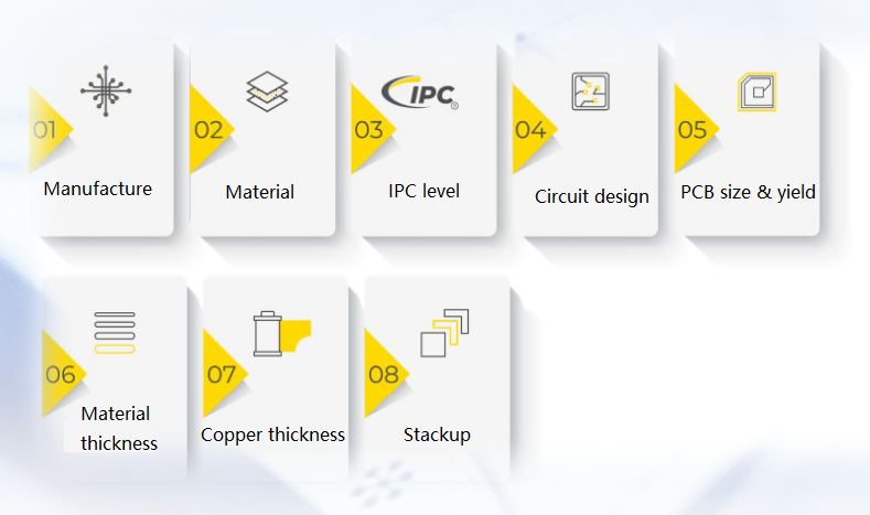
1. Type of manufacturing process
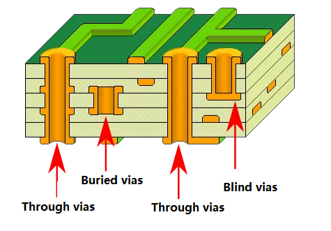
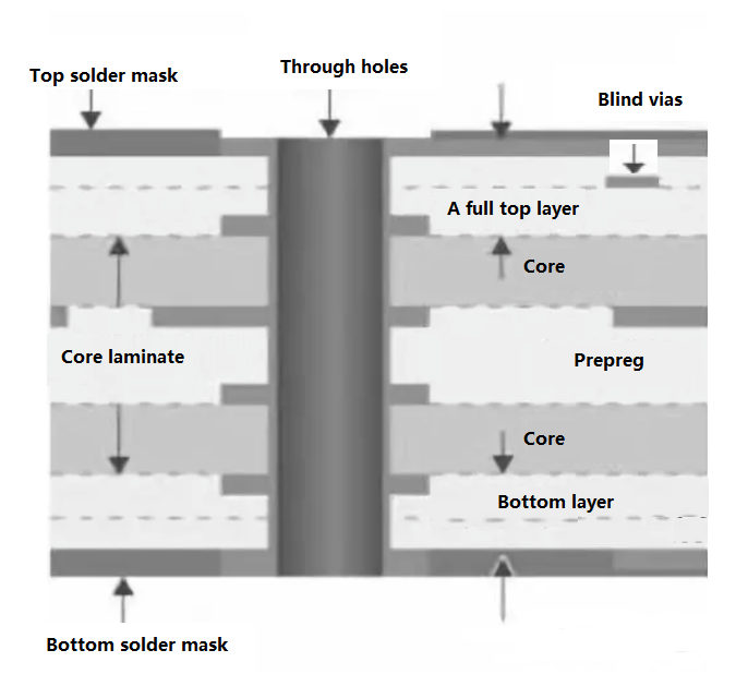
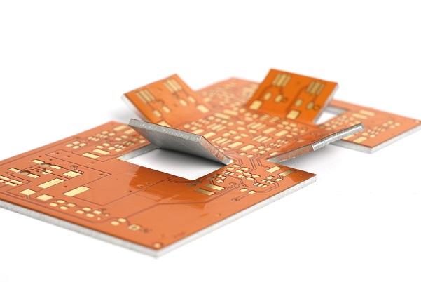
The technical type of PCB determines its complexity and cost. For example, simple single panels cost much less than multi-layer panels, while flexible circuits (FPC) or rigid and flexible panels require more complex manufacturing processes and naturally cost more. In addition, whether advanced technologies such as microvias, laser drilling, blind holes or buried holes are required can also have a significant impact on the quotation.
2. Material type
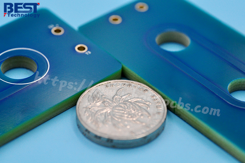
Materials are an important part of PCB costs. Common materials include FR4, ceramics, metal substrates, etc. FR4 is the most common base material and is suitable for most conventional applications, but for high-frequency, high-temperature environments, ceramic or metal-based materials may be more suitable, but their price is relatively high. Choosing the right material not only affects the performance, but also directly affects the cost.
3. IPC level
IPC grades reflect the quality standards of PCB manufacturing, commonly used are IPC-A-600 grades 1, 2 and 3. The higher the grade, the more stringent the manufacturing requirements, and the corresponding increase in cost. For example, grade 3 PCBS are usually used in high-demand fields such as aerospace and medical equipment, which require higher accuracy and quality control, so the price is higher.
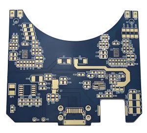
4. Circuit design
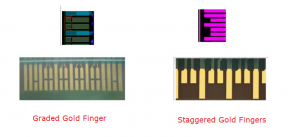
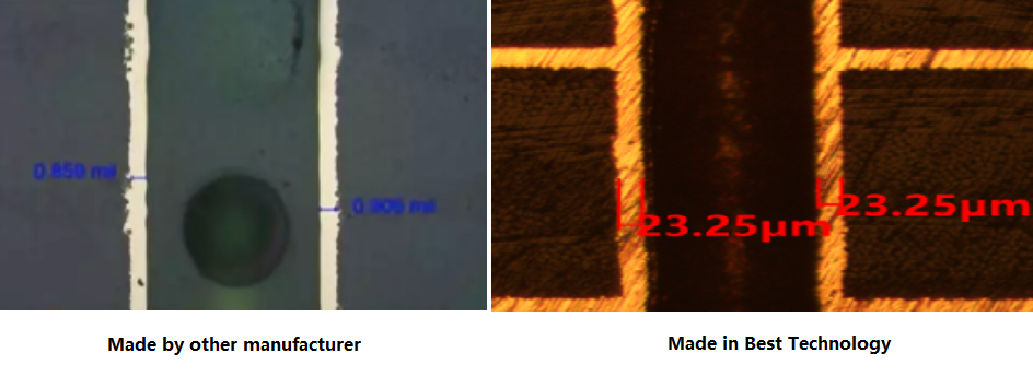
PCB circuit design complexity directly affects manufacturing costs. Including wire width, spacing, hole size and so on, the production process has put forward different requirements. High density interconnect (HDI) boards typically require more elaborate wiring techniques and may involve the use of microvias, which will increase the difficulty and cost of manufacturing.
5. PCB size and yield
The size of the PCB directly affects the amount of material used, and the larger the board, the more material is needed. In addition, the yield is also an important factor affecting the quotation. PCB manufacturing with complex design or high density lines is prone to defects, resulting in decreased yield. That means manufacturers may need to produce more boards to meet orders, increasing costs.
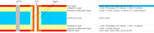
6. Material thickness
Different applications require different thicknesses of PCB materials. The standard FR4 thickness is usually 1.6mm, but thinner or thicker boards are sometimes used. Changes in material thickness can affect the overall cost, especially if thicker sheets require special processing or higher strength, and manufacturing expenses will increase accordingly.
7. Copper thickness
The copper thickness in the PCB usually has a standard choice, such as 1oz, 2oz or even thicker copper layers. The higher the copper thickness, the better the conductivity of the PCB, suitable for high-current applications, but the increase in copper thickness will significantly increase the manufacturing cost, especially in the plating and etching process requires additional materials and processes.
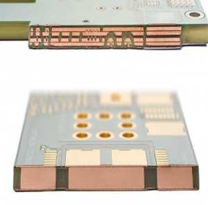
8. Stack-up method
The stacking mode determines the number of layers and the interlayer structure of the PCB. Complex multilayer boards or HDI boards require more complex lamination processes. For example, the lamination method may involve multiple pressing, the use of prepregs or special insulation materials. Each additional layer requires more manufacturing steps, resulting in increased costs.
9. Quantity
The quantity of the order has a direct impact on the PCB quotation. High-volume production can reduce unit prices by spreading tooling and setup costs, while small-batch orders are typically more expensive due to relatively high production preparation and start-up costs.
10. Delivery date
The shorter the delivery time, the higher the quotation. Rush orders require prioritizing production, which can disrupt the plant’s production schedule and require additional resource deployment. To meet urgent delivery deadlines, manufacturers may need to work overtime or speed up production, increasing overall production costs.
These are just a few examples, but they show how engineering considerations are woven into every part of the quoting process.
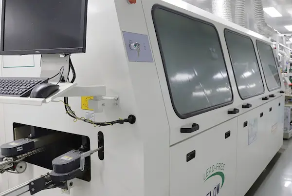
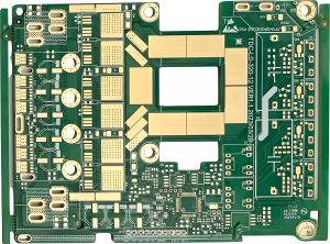
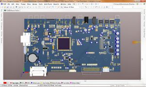
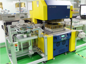
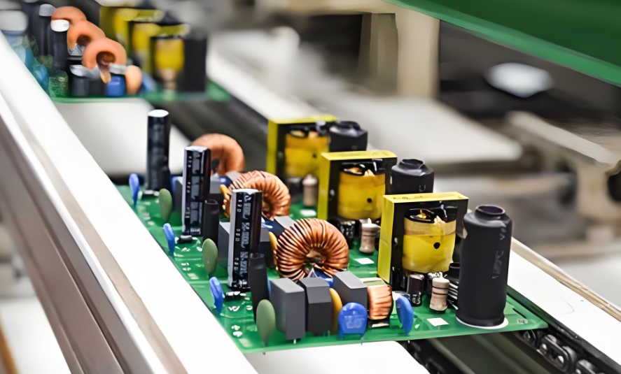
PCB Manufacturing Process
How Do Engineers Calculate PCB Manufacturing Costs?
Engineers calculate PCB manufacturing costs by considering the design specifications and the production methods needed to meet those requirements. They start by analyzing the PCB’s layout and design, which determines factors like layer count, trace width, and hole size. Each of these elements has a direct impact on the materials used and the manufacturing process.
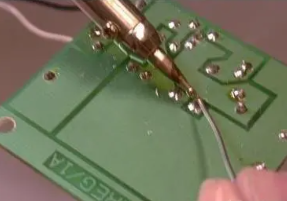
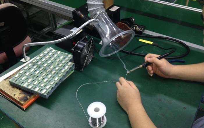
They also consider the assembly process—whether it’s surface-mount or through-hole—and what testing will be required. After evaluating these details, they calculate the costs associated with each step of the manufacturing process. This ensures the final quote is both accurate and comprehensive.
What Type of Engineer Designs PCBs?
Engineers who design PCBs typically have a bachelor’s degree or above in electrical engineering, automation, computer science, or a related field and understand the basics of electronic design, printed circuit board (PCB), and electronics manufacturing in the PCB industry. These engineers need to master PCB design software such as Altium Designer, Eagle PCB, PADS, or CAD, etc., as well as the use of related manufacturing and testing tools. At the same time, they need to have a knowledge of the PCB industry, a certain circuit design and electronic components knowledge, including digital and analog circuits, signal processing, power electronics, embedded systems, communication technology, etc. In addition, holding certificates such as IPC-2221/2222, IPC-A-600/610, and CID (Certified Interconnect Designer) can prove that they have relevant professional knowledge and skills, which can help improve their career competitiveness.
These engineers also need to have a strong sense of responsibility and team spirit, have good communication and coordination skills, and be able to work effectively with customers, manufacturers, and other team members. For junior engineers, it is recommended to study in a single point of depth, such as PCB design, SI simulation, thermal design, EMC design, product testing, etc., and then start from this advantage point to expand the scope of knowledge
What Materials Are Considered During PCB Quote Packaging?
The type of material used for a PCB is a major cost driver. Common materials include:
- FR4
This is the most common material used in PCBs due to its balance of cost and performance. It’s versatile and reliable for most standard applications.
- Metal Core
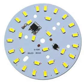
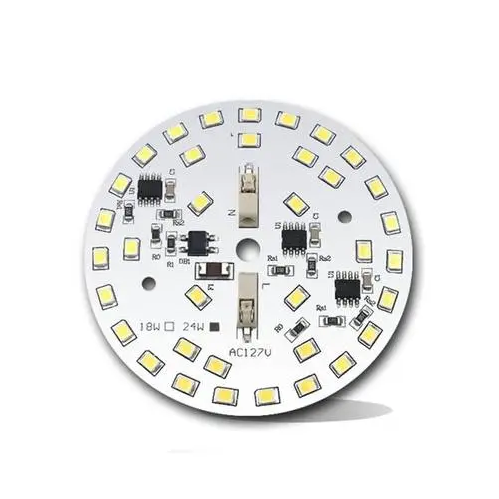
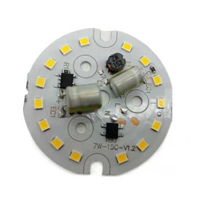
Metal core PCBs are used in applications where heat dissipation is a concern, such as LED lighting. These boards are more expensive due to the metal layer.
- Ceramic
Ceramic materials are used for high-frequency or high-temperature applications. They are more costly but offer better performance in extreme conditions.
Each material has its own manufacturing process, which also affects the cost. For instance, metal core boards may require different drilling techniques compared to standard FR4 boards. Engineers must consider these details when preparing a quote.
How Does the Choice of PCB Manufacturing Methods Impact the Quote?
The method used to manufacture the PCB can greatly impact the final cost. Common methods include:
- Surface-Mount Technology (SMT): This is the most common method for modern PCB assembly. It’s efficient and cost-effective for most applications.
- Through-Hole Technology (THT): This method is used for components that require a stronger mechanical bond. It’s more labor-intensive and, therefore, more expensive.
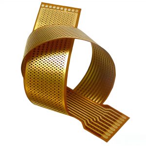
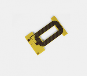
- Flexible and Rigid-Flex Manufacturing: These types of PCBs require specialized processes and materials, which can increase the cost.
Additionally, advanced techniques like laser drilling for microvias or selective soldering for complex assemblies may be necessary for high-precision designs. Each of these methods requires careful consideration, and engineers must choose the best process for both the design and the budget.
Who Designs PCB?
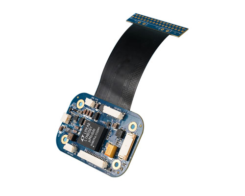
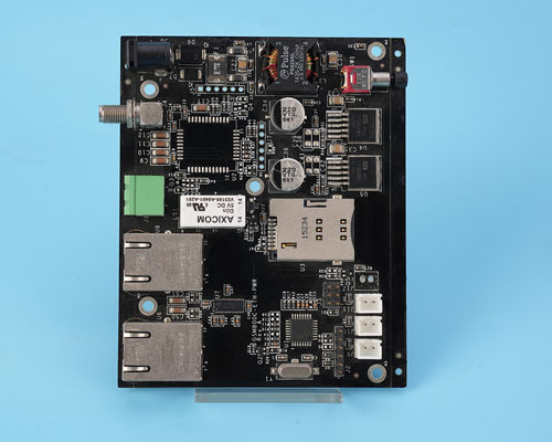
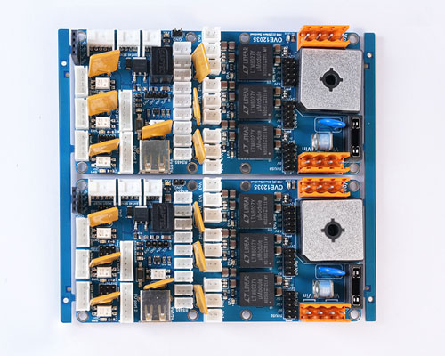
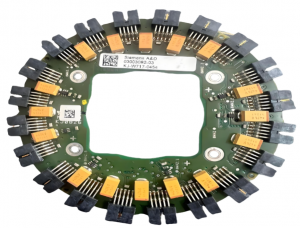
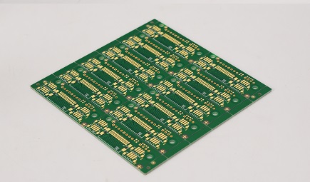
Since 2006, EBest Circuit (Best Technology) has been the leading PCB quick turn manufacturer specializing in both PCB prototype and production quantities, initially produced single-sided and double-sided printed circuit boards for the consumer electronics market. Now, we provide not only FR4 PCB, but also some special PCB like flex circuit, metal core PCB, ceramic PCB, extra thin PCB, HDI PCB, IC substrate, busbar PCB, heavy copper PCB and so on. We can make 50 layers PCB, and it is not our limit.
Nowadays, EBest Circuit (Best Technology) has grown to become a major PCB manufacturer in Asia to serve in diverse customers base such as electronics appliance, communication, educational electronics, power supplies, automations.
For more information about PCB, or to learn more about the online quote and ordering process, please visit www.bestpcbs.com