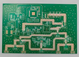
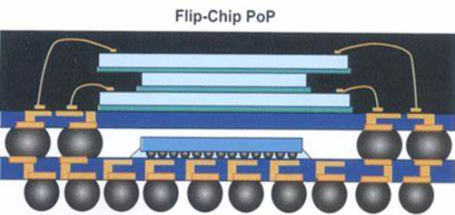
What is smt pop process?Package on Package (PoP) means that a logical package with high integration at the bottom is superimposed on another matching large-capacity memory package to form a new package as a whole. Laminated packaging can be the same shape of the logic and memory chip package can be reintegrated, without the use of stacked logic-memory chip packaging method in the manufacturing and commercial problems. This new form of high-density packaging is mainly used in a variety of consumer electronic products such as smart phones, digital cameras, and portable wearable devices.
What Does POP Do in Assembly?
In an era where consumer electronics are becoming smaller and more powerful, saving PCB space is crucial. PoP allows for the vertical stacking of components, such as processors and memory, on top of each other. This is especially important in devices like smartphones, tablets, and wearable technology, where space is at a premium.
One of the significant advantages of PoP is the ability to individually test and replace the stacked components before final assembly. This step-by-step verification ensures higher yields during manufacturing, as defective components can be identified and replaced early in the process. Additionally, since each component is tested separately, the overall cost of assembly can be reduced, as fewer defective products reach the final stages of production.
Moreover, PoP provides manufacturers with the flexibility to mix and match different types of components. For example, different memory types can be combined with various processors, depending on the requirements of the final product.
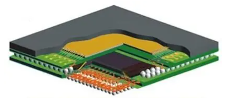
SMT POP Structure
POP stacking assembly typically involves placing components on top of each other, usually combining logic and memory devices. The structure can range from 2 to 4 layers, with memory PoP going up to 8 layers. Although the overall height increases slightly, each component can be tested individually before assembly, ensuring higher yield rates and minimizing total assembly costs.
PCB Assembly Layers of PoP:
Amkor PoP Typical Structure:
Bottom PSvfBGA (Package Stackable very thin fine pitch BGA)
Top Stacked CSP (fine pitch BGA)
Bottom PSvfBGA Structure:
Dimensions: 10-15mm
Pad pitch: 0.65mm, with bottom ball pitch at 0.5mm (0.4mm)
Substrate: FR-5
Ball material: 63Sn37Pb/Pb-free
Top SCSP Structure:
Dimensions: 4-21mm
Bottom ball pitch: 0.4-0.8mm
Substrate: Polyimide
Ball material: 63Sn37Pb/Pb-free
Ball diameter: 0.25-0.46mm
SMT POP Manufacturing Process
The manufacturing process for Package on Package technology is a multi-step procedure that demands precision and careful attention to detail to ensure the successful assembly of high-performance electronic devices. Here’s an extended explanation of each stage in the PoP manufacturing process:
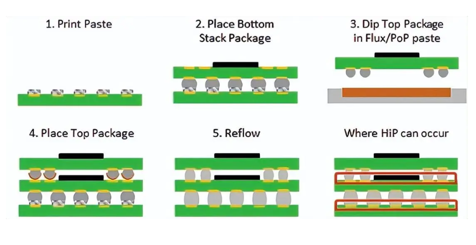
1. Non-PoP Side Component Assembly
The PoP process begins with the assembly of components on the non-PoP side of the PCB. This involves standard SMT assembly processes:
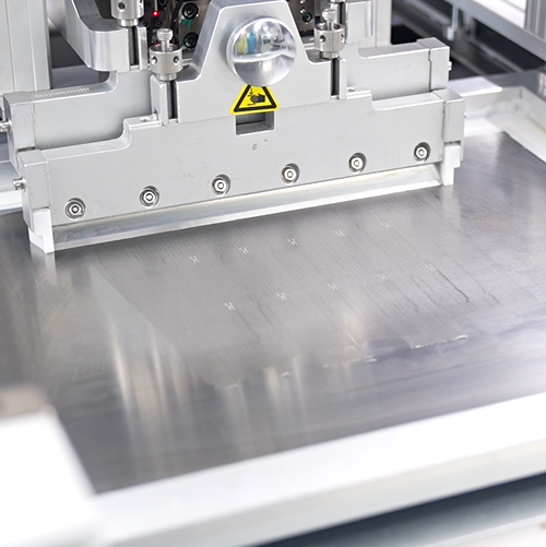
- Stencil Printing: Solder paste is applied to the designated pads on the PCB using a stencil.
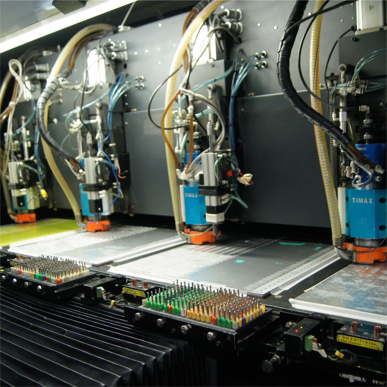
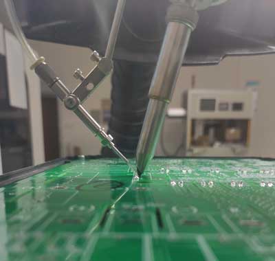
- Component Placement: Using automated pick-and-place machines, surface-mount components are accurately positioned onto the solder-pasted pads.
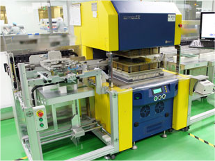
- Reflow Soldering: The PCB is then passed through a reflow oven, where the solder paste is heated to its melting point, securing the components to the board.
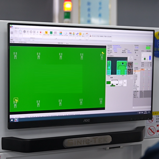
- Inspection: The solder joints are inspected using Automated Optical Inspection (AOI) to ensure that they are correctly formed and that the components are properly placed.
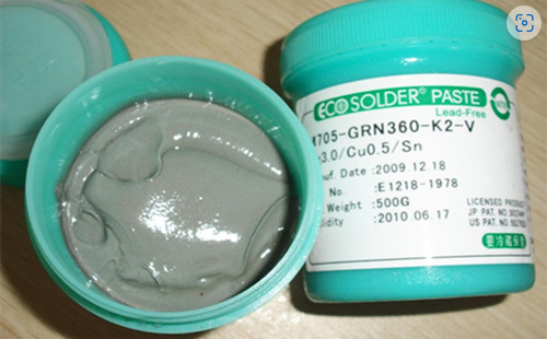
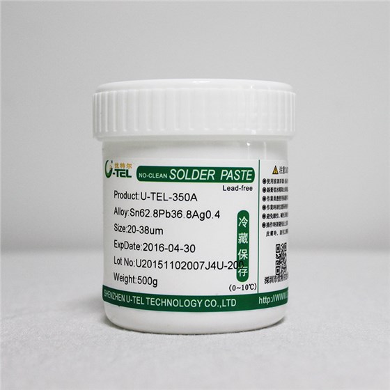
2. Solder Paste Printing on the PoP Side
After completing the assembly on the non-PoP side, the PCB is flipped, and solder paste is printed on the pads where the bottom PoP component will be placed. This step is crucial, as the quality of the solder paste application directly affects the integrity of the solder joints between the PoP components.
3. Placement of Bottom Components and Other Devices
The bottom components, which typically include the logic processor, are placed onto the solder-pasted pads using high-precision pick-and-place equipment. This placement must be extremely accurate to ensure proper alignment with the top component in the subsequent steps.
4. Flux or Solder Paste Dipping for the Top Components
Before the top component is placed, it is dipped in flux or a thin layer of solder paste. This dipping ensures that the solder joints between the top and bottom components are robust and reliable. The flux helps to clean the surfaces and promote better solder flow during reflow, while the solder paste provides additional material for the solder joints.
5. Placement of Top Components
The top component, typically a memory chip, is then placed onto the bottom component. This step requires precise alignment to ensure that the solder balls on the top component correctly match the pads on the bottom component. Any misalignment can lead to defective connections and, consequently, a malfunctioning device.
6. Reflow Soldering and Inspection
Once the top component is placed, the entire assembly is subjected to reflow soldering. During this process, the PCB passes through a reflow oven where the solder paste re-melts, forming solid connections between the components. The temperature profile during reflow must be carefully controlled to prevent warping or damaging the delicate PoP structure.
After reflow, the assembly is inspected using AOI or X-ray inspection to verify the quality of the solder joints, particularly the hidden joints between the top and bottom components. X-ray inspection is often employed because it can penetrate the layers and provide a clear view of the solder joints, ensuring there are no voids, misalignments, or insufficient solder.
7. Final Testing and Quality Control
The assembled PoP structure undergoes a series of electrical tests to ensure functionality. This includes testing for continuity, shorts, and the performance of the integrated components. High-quality PoP assemblies should pass all functional tests without issue, confirming that the solder joints and component placements are reliable.
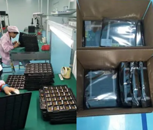
8. Packaging and Shipping
After passing the final tests, the PoP assemblies are cleaned to remove any residual flux or contaminants. They are then packaged according to the customer’s requirements and prepared for shipping. Proper packaging is essential to protect the sensitive PoP structures from damage during transit.
POP Design Considerations
Factors affecting the spatial relationship include substrate and component design, substrate manufacturing processes, component packaging processes, and SMT assembly processes. Key aspects to consider are:
- Pad design
- Solder mask opening
- Ball size and height variation
- Amount of flux or solder paste applied
- Placement accuracy
- Reflow environment and temperature
- Warpage of components and substrate
- Bottom component molding thickness
What are the advantages of POP smt process?
POP is mainly a system integration 3D package developed for mobile devices, and its structure mainly has the following characteristics.
- Storage devices and logic devices can be freely combined, and can be tested or replaced separately to ensure the yield.
- POP is stacked in the vertical direction, saving the board area and improving the system packaging density.
- The vertical interconnection of stacked devices replaces the traditional two-dimensional package interconnection, which can realize faster data transmission between logic devices and storage devices.
With the development of technology, the following main types of POP structures have emerged.
- Solder Ball Connected PoP
Logic chips have more I/0 ports, so they are often packaged with Flip Chip (FC) technology and used as the bottom component. The bottom chip adopts Capillary Under Fill (CUF) technology.
- MLP Connected PoP
In order to develop a thinner PoP Package structure, MoldimgLaser Package (MLP) technology came into being, also known as Through Mold Via (TMV) technology on the market. The method is to first weld the tin ball around the bottom chip and directly plastic seal, and then use laser perforation to expose the tin ball for subsequent connection with the upper components.
- Folded and BVA Connected PoP
In order to meet the requirements of thin size, strong function and large I/0 number of PoP products, flexible circuit boards are used to connect various package components and fold to form PoP structure, and BVA (Bond Via Array) is used to improve product performance and reduce pin spacing.
POP Applications
1. Smartphones: PoP is widely used in smartphones, like the Meizu 16S, for integrating application processors and memory.
2. Wearable Devices: PoP is commonly used in next-generation wearable devices.
3. Electronic Watches: PoP packaging is key for improving performance and reducing costs in electronic watches.
4. Earphones: The Meizu POP Pro noise-cancelling earphones utilize PoP technology.
5. Health Watches: Huami’s Amazfit Pop, one of the most affordable blood oxygen monitoring watches, uses PoP technology.
For more information about our POP Assembly capabilities, please contact us any time! We can be reached via email at sales@bestpcbs.com, or toll free at +86-755-2909-1601.