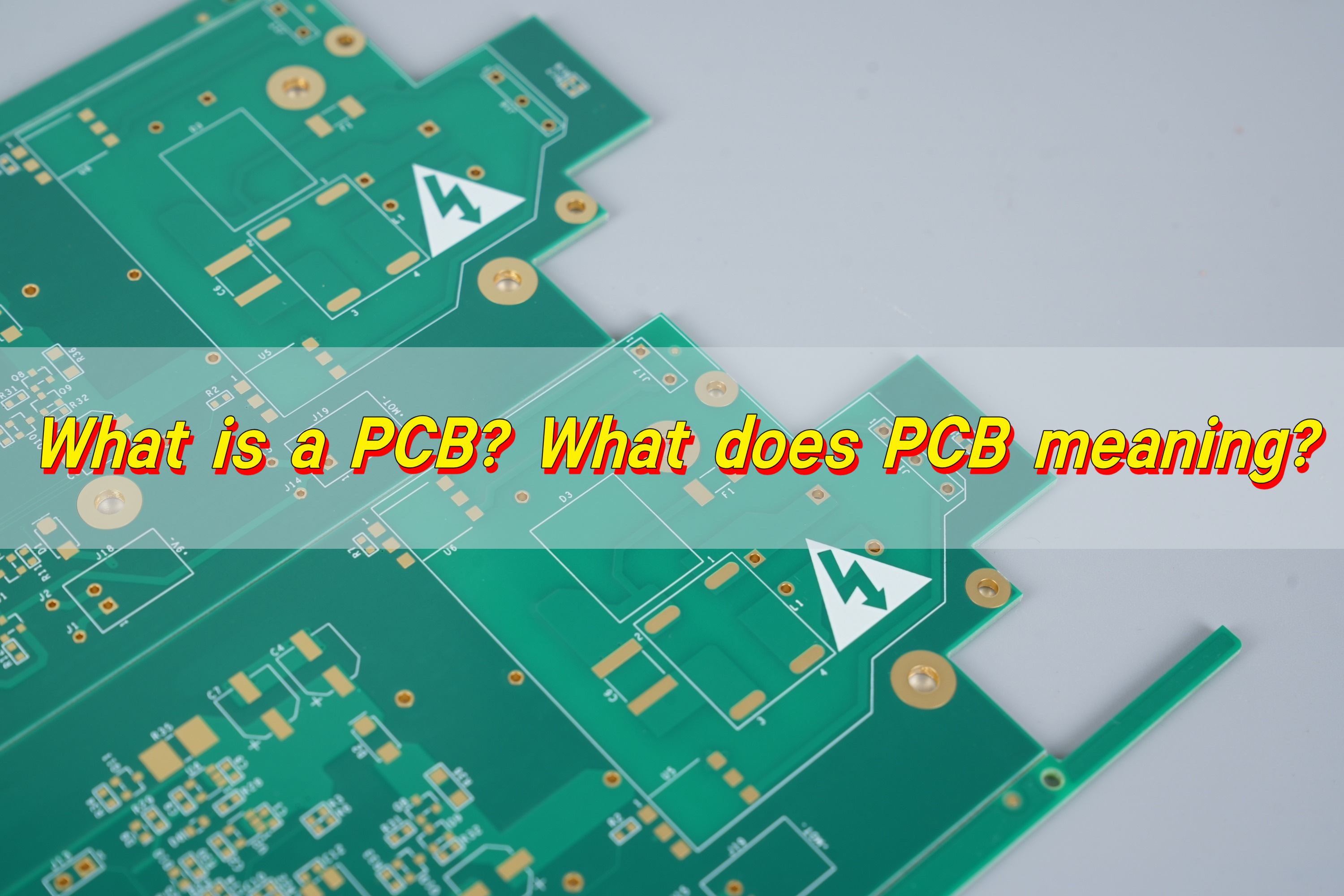
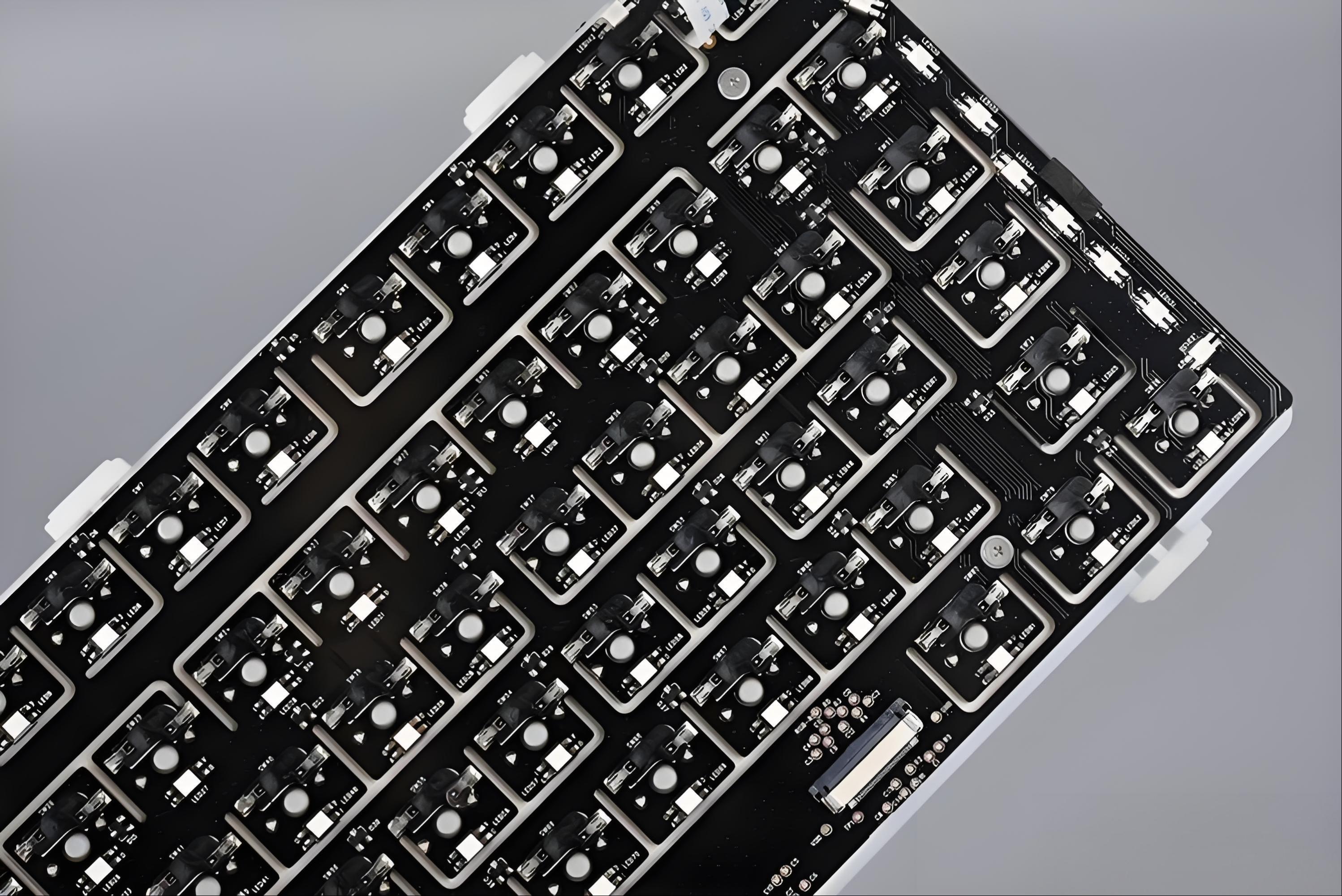
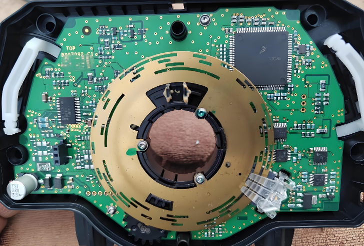
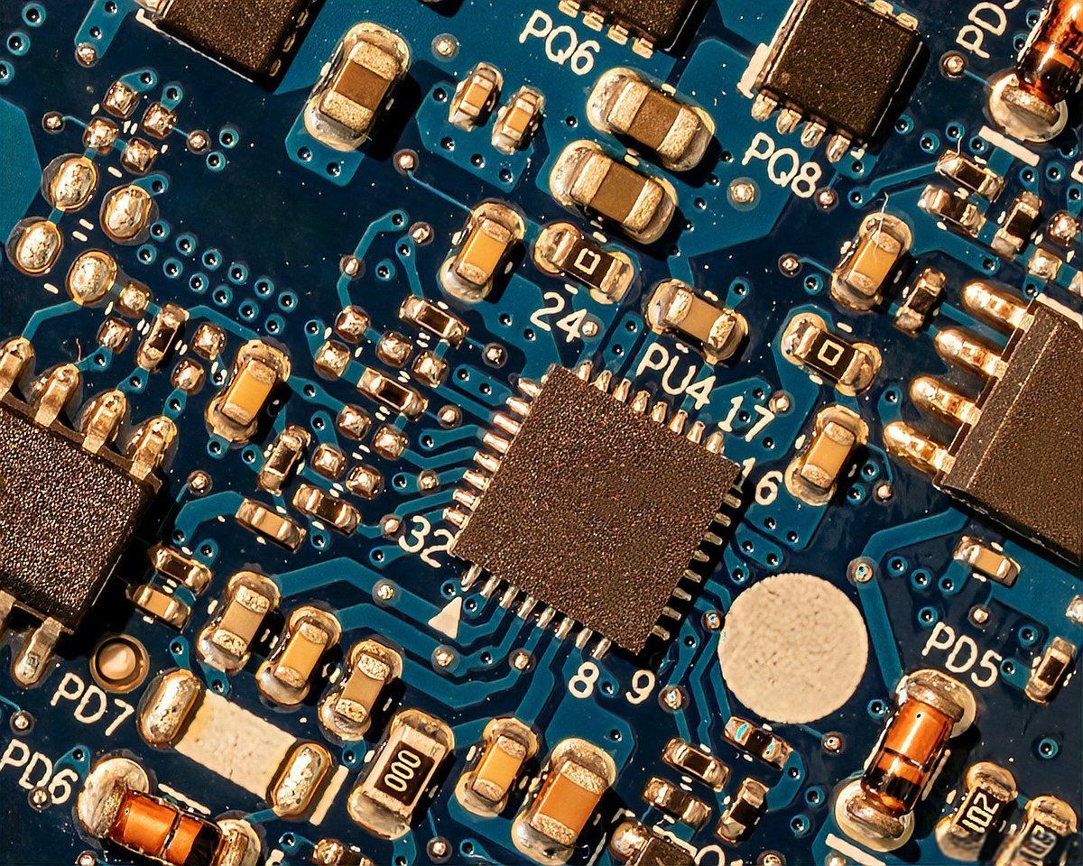
Identifying parts on a circuit board becomes much easier once you understand the visual patterns, silkscreen labels, and common symbols printed on every PCB. Most boards follow the same naming rules: R for resistors, C for capacitors, L for inductors, Q for transistors, U for ICs, and D for diodes.
What Are All the Parts of a Circuit Board?
Circuit board hosts a wide range of components, and each part plays an essential role. These tiny pieces work together to drive the entire device. Even simple electronics carry dozens of unique pieces, while advanced boards hold hundreds.
At a glance, the most common parts on a circuit board include resistors, capacitors, inductors, diodes, LEDs, connectors, sockets, ICs, transistors, voltage regulators, oscillators, crystals, relays, switches, and heat sinks. Some PCBs include sensors, antennas, or RF sections, depending on their purpose.
Below is a more detailed explanation to help you spot them easily.
- Resistors
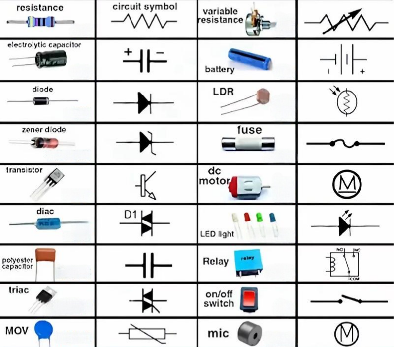
Resistors help manage current. They keep signals stable, reduce excess flow, and shape how electricity moves. They appear as small rectangular chips during surface-mount construction. Through-hole versions use color bands to indicate resistance values. Their board marking starts with “R”.
- Capacitors
Capacitors store and release energy. They calm noise, filter signals, and smooth voltage. Ceramic capacitors look like small beige or brown blocks. Electrolytic versions appear as cylinders. They carry “C” as their identifier.
- Inductors
Inductors generate magnetic fields and regulate energy flow in power circuits. They might look like coiled wires, small blocks, or shielded cubes. Their symbol is “L”.
- Integrated Circuits (ICs)
ICs handle logic, memory, control, processing, and communication. They often act as the “brain” of the board. These appear as black chips with multiple pins. Their symbol is “U”.
- Transistors
Transistors amplify or switch signals. They control high and low outputs. You’ll see them labeled as “Q”.
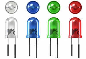
- Diodes and LEDs
Diodes allow current to move in one direction. LEDs emit light for indication. Their identifier is “D”.
- Connectors
Connectors give access to power, data, sensors, modules, or external inputs. They can be simple pin headers, USB ports, sockets, or spring connectors. They appear as “J”.
- Crystals and Oscillators
These create timing signals. They help ICs stay synchronized. They are often oval, metal-covered parts marked “Y” or “X”.
- Voltage Regulators
These control the level of voltage sent to other parts. They protect sensitive components. They appear as “U” or “VR”.
- Fuses
Fuses shield the board from overload. They break the circuit when current rises too high. You will see “F”.
- Switches and Buttons
These send user-controlled commands. They give feedback through physical press.
Each component supports stability, safety, and communication between circuits.
Types of Parts on a Circuit Board
To identify parts more easily, it helps to sort them into categories.
- 1. Passive Components
These operate without needing external power. Passive parts manage noise, shape signals, and ensure smooth operation.
- Resistors
- Capacitors
- Inductors
- Ferrite beads
- Transformers (many versions)
- 2. Active Components
These require a power source. Active parts create calculation, logic, switching, and amplification functions.
- Transistors
- Microcontrollers
- Integrated circuits
- Voltage regulators
- Operational amplifiers
- 3. Electromechanical Components
These involve physical force. They help the product interact with users and external systems.
- Switches
- Relays
- Connectors
- Buttons
- Sockets
- 4. Protection Components
These guard the board from overload and stress. They protect sensitive electronics from damage.
- Fuses
- TVS diodes
- Resettable fuses
- Varistors
- Thermistors
- ESD protectors
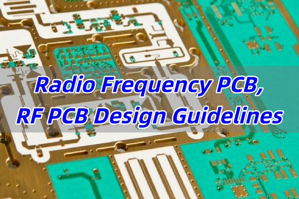
- 5. RF and Communication Components
These support wireless communication. Many modern devices rely heavily on these.
- Antennas
- Filters
- RF shields
- Baluns
- Matching networks
With this classification, identifying parts on a circuit board becomes much easier. Each group serves unique roles, and many boards share similar arrangements.
How to Identify Components on a Circuit Board?
Here is a detailed breakdown that helps anyone—from beginners to technicians—identify components accurately.
- 1. read the Silkscreen Labels
Every PCB has printed markings that guide you. Below are the most common symbols:
- R → resistor
- C → capacitor
- L → inductor
- D → diode
- Q → transistor
- U → integrated circuit
- J → connector
- TP → test point
- F → fuse
- FB → ferrite bead
- SW → switch
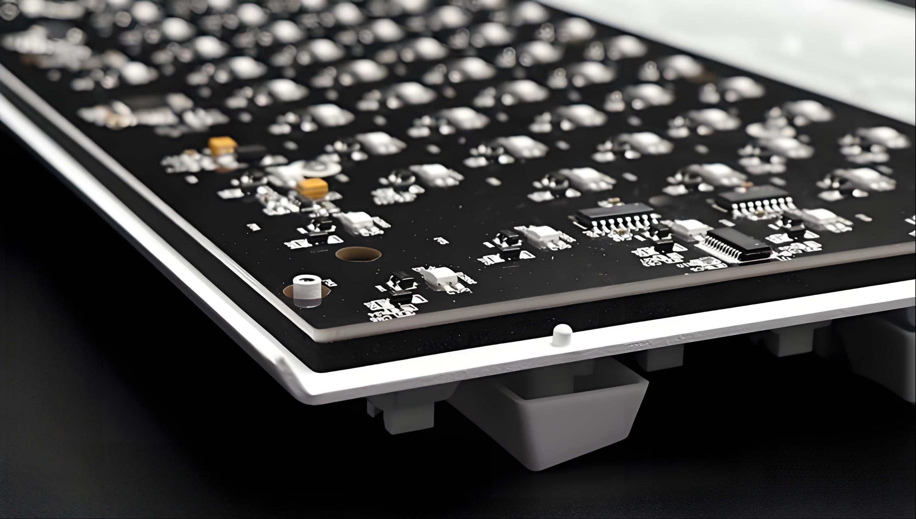
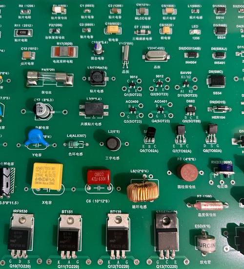
- 2. Identifying by Shape
Components have signature shapes that make them recognizable:
- Resistors → tiny rectangles
- Ceramic capacitors → small blocks
- Electrolytic capacitors → tall cylinders
- Inductors → dark cubes or coils
- Diodes → narrow cylinders or SMD blocks with stripe
- Transistors → three-pin packages
- ICs → black rectangular chips
- Crystals → silver oval housings
- Connectors → white or black plastic structures
- 3. Count the Pins
The number of pins can help you identify the part even without reading the label.
- 2-pin parts → resistors, capacitors, diodes
- 3-pin parts → transistors, regulators
- 8 to 64 pins → ICs, amplifiers, controllers
- Large multi-pin → connectors, sockets
- 4. Check Polarity
Some parts have direction or polarity.
- Diodes show a line marking
- Electrolytic capacitors display a minus stripe
- LEDs have a flat edge
- ICs show a dot or notch for pin 1
- 5. Use a Circuit Board Diagram
A circuit board parts diagram shows every component and its location. It simplifies repair and troubleshooting.
- 6. Refer to PCB Components Symbols
Schematics can guide you when identifying components. These symbols follow global standards and remain consistent across every device.
What Three Major Components Are Needed in a Circuit?
Every circuit needs three key building blocks. Even the most complex electronics trace back to these three essentials.
- 1. Power Source
The circuit needs a source of energy. This might be a battery, power supply, or charger.
- 2. Load
The load uses energy to perform work. This includes LEDs, motors, heaters, sensors, and speakers.
- 3. Connections
Wires or copper traces link the parts together. These create a full path for current.
These three parts appear in every circuit, from simple toys to advanced medical devices. PCB layouts simply organize them in more advanced ways.
What Parts of a Circuit Board Are Valuable?
This is common among repair technicians, recyclers, and hobbyists.
Here are parts considered more valuable:
- Integrated Circuits (ICs): Chips like microcontrollers, CPUs, GPUs, memory, RF transceivers, or power ICs carry more value because of advanced features.
- Gold-plated Connectors: Many connectors contain gold plating for conductivity and reliability. Gold layers are thin but collectible.
- High-Frequency Components: Filters, oscillators, RF amplifiers, and antennas come with higher cost.
- Power Components: MOSFETs, IGBTs, drivers, transformers, and regulators often cost more.
- Sensors: Temperature, pressure, motion, optical, and other sensors have high commercial value.
While the entire board contributes to performance, these parts stand out as more expensive during repair or recycling.
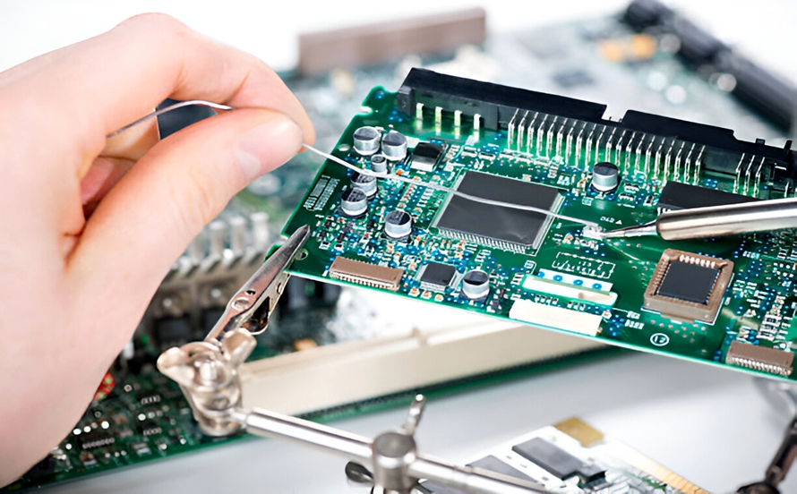
How to Replace a Part on a Circuit Board?
Replacing a component on a PCB sounds challenging, but the process becomes easy once you follow clear steps.
Here is a practical guide:
- 1. Diagnose the Fault
Use visual inspection. Burn marks, swelling, leakage, or broken joints often indicate failure.
- 2. Identify the Component
Check the silkscreen label. Make sure you note the exact model, value, package size, and polarity.
- 3. Remove the Old Part
Soldering iron or hot air can remove parts. For small parts, tweezers help lift them gently.
- 4. Prepare the Pads
Clean leftover solder. Wipe the pads gently with solder wick to achieve a smooth surface.
- 5. Place the New Part
Align accurately with polarity and orientation. Poor alignment can cause failure.
- 6. Solder the New Part
Heat the pads and add a small amount of solder. The connection should look shiny, smooth, and firm.
- 7. Test the Board
Turn on the power. Measure the circuit to confirm stable operation.
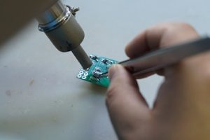
How to Solder Parts on a Circuit Board?
Soldering is one of the most important skills for working with PCBs. Good soldering makes the board stable and durable.
- 1. Prepare Tools
- Soldering iron
- Solder wire
- Flux
- Tweezers
- Solder wick
- Isopropyl alcohol
- 2. Apply Heat
Warm the pad and the pin evenly. This helps solder flow smoothly.
- 3. Add Solder
Touch the solder wire to the joint. Use only the amount needed.
- 4. Inspect the Joint
A strong joint looks smooth and clean. Avoid dull or cracked joints.
- 5. Clean the Area
Remove flux residue with alcohol for a neat finish.
Good soldering gives the board longer life and better performance.
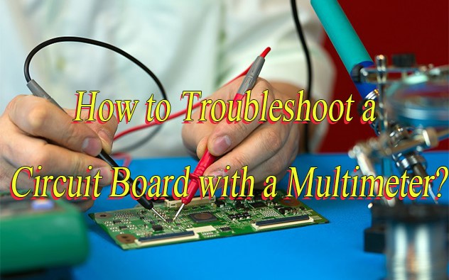
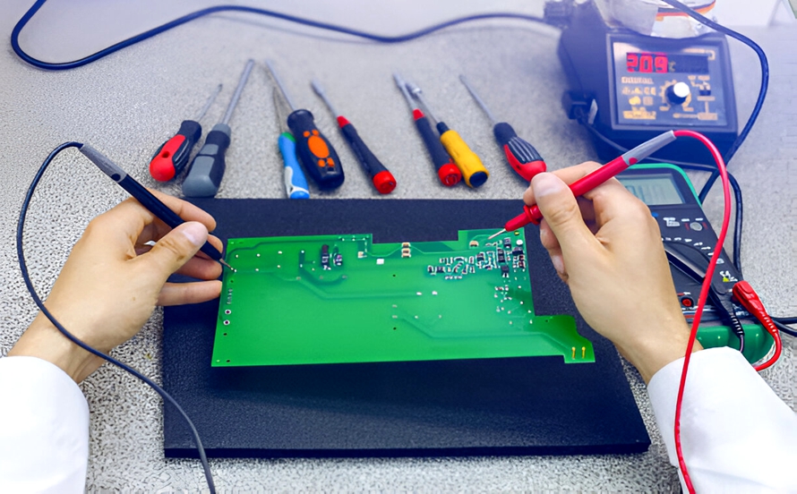
How to Test Parts on a Circuit Board?
Testing helps you confirm whether components are healthy. A digital multimeter works well for this job.
- 1. Testing Resistors
Set meter to resistance. Touch both ends. Compare reading with labeled value.
- 2. Testing Capacitors
Use capacitance mode. Some small capacitors may show minor variation.
- 3. Testing Diodes
Set diode mode. Forward direction should show a value. Reverse should show none.
- 4. Testing Transistors
Check each pin for forward and reverse bias. Many meters include transistor sockets.
- 5. Testing ICs
ICs often require powered testing. Use voltage readings, probe signals, or test points.
- 6. Testing Inductors
Check for continuity. Stable reading indicates a good coil.
- 7. Testing Connectors
Inspect each pin for continuity and firm contact.
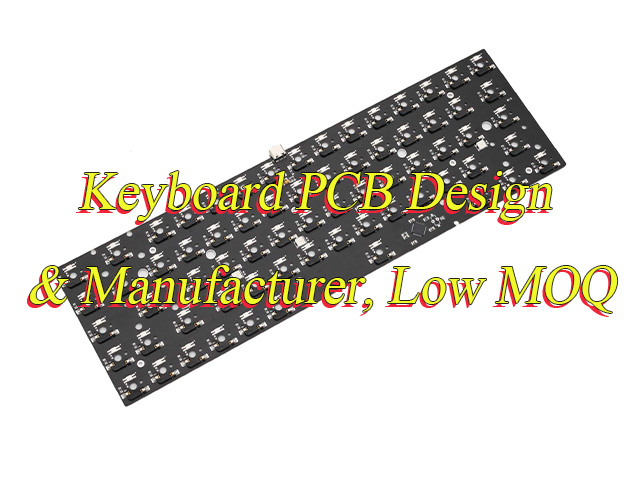
If you need PCB, PCBA, or engineering support, EBest Circuit (Best Technology) provides reliable fabrication and assembly solutions. Our team supports sample builds, mass production, component sourcing, and technical analysis with strict quality control and powerful manufacturing capability.
For inquiries or custom projects, contact: sales@bestpcbs.com