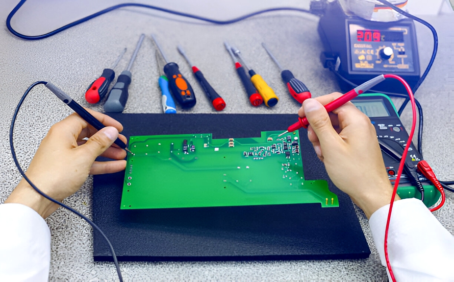
A PCB continuity test uses a multimeter to check whether two selected points are electrically connected on an unpowered board. The displayed resistance and the expected circuit path determine whether the result is normal; a beep alone cannot prove that a trace is good or that two nets are shorted.

What Is a PCB Continuity Test and What Can It Tell You?
A continuity test measures whether the resistance between two probe points is below the meter’s reporting threshold. The meter does not know whether the path is the intended copper trace, a component, a parallel branch, contamination, or an unintended solder bridge. The circuit design must supply that meaning.
- Intended connection: Two points on the same net should normally show a low and stable resistance when no series component is expected between them. Compare the result with the measured lead baseline and repeat from a second accessible point before accepting the route.
- Open path: A trace crack, lifted pad, unseated connector, broken via, damaged cable, or unsoldered joint may produce OL, an unexpectedly high resistance, or a reading that changes with permitted movement. Divide the route into sections to separate a real break from poor probe contact.
- Unintended connection: Nets that should be isolated may show low resistance because of a solder bridge, conductive debris, moisture, contamination, or internal damage. Confirm the schematic relationship and isolate approved branches before deciding that the low reading is a physical short.
- Component path: Windings, fuses, shunts, inductors, transformers, switches, and low-value resistors can legitimately trigger the tone. Identify every component between the probes and measure the numerical resistance or polarity behavior instead of judging the path by sound alone.
The most useful result is therefore not “beep” or “no beep.” It is a documented comparison between the measured endpoints, the expected circuit relationship, the measured resistance, and the conditions under which the reading was taken.
What Should You Check Before Testing PCB Continuity?
Prepare the board, meter, and test plan before touching the probes to the PCB. These checks prevent meter damage, false readings, accidental shorts, and unnecessary rework:
- Remove and verify power: Disconnect every external supply, powered cable, and battery. Use voltage mode to confirm that the selected points are not energized before switching to continuity or resistance mode. The Fluke continuity testing guide likewise requires a de-energized circuit.
- Control stored energy: Discharge capacitors only by the product’s approved service method, then recheck the relevant rails. Do not assume that unplugging the unit removes stored voltage.
- Define the expected relationship: Use the schematic, netlist, layout, connector pinout, and board revision to identify both test points and decide whether they should be connected, isolated, or linked through a component.
- Establish the meter baseline: Confirm the correct lead terminals and continuity function. Touch the probe tips together and record the lead resistance and audible response, then separate them and verify the open indication.
- Choose safe access points: Use fine, insulated probes on test pads, component pads, vias, or connector pins without bridging adjacent conductors. Support the PCB so probe force does not flex it.
- Record the board state: Note connected cables, switch positions, installed modules, and any isolated branches. Change one condition at a time and record it so an apparent fault can be reproduced and the board can be restored correctly.
How Do You Perform a PCB Continuity Test with a Multimeter?
Test one defined electrical relationship at a time. The sequence below preserves the original board condition, establishes a meter baseline, and records the resistance needed to distinguish an intended connection from a false short or an open path.
Step 1: Identify the two test points. Mark both endpoints and state whether they should be connected or isolated. Note any resistor, coil, connector, switch, jumper, or protection device between them.
Step 2: Remove power and stored energy. Disconnect supplies and batteries, follow the approved discharge method, and verify the absence of voltage at the relevant rails.
Step 3: Select continuity mode. Place the leads in the correct terminals and select the continuity function. If the meter combines several functions, confirm that the continuity symbol is active.
Step 4: Verify the probes. Touch the tips together and note the lead resistance and tone, then separate them and confirm the open indication.
Step 5: Place the probes on the intended points. Contact exposed test points, pads, terminals, or connector pins without touching neighboring conductors. Do not scrape solder mask merely to create access.
Step 6: Read the resistance and audible indication. Hold both tips steady and note the displayed value, tone, stability over time, board state, and any isolated branches.
Step 7: Compare the result with the design. If it disagrees with the expected net relationship, retest from a second accessible point before rework. One poor probe contact can imitate an open.
Continuity mode is suitable for a connection or isolation question on an unpowered circuit. It does not verify a powered signal, controlled impedance, insulation resistance at a specified voltage, or operation under load.
How Should You Interpret PCB Continuity Test Results?
The displayed resistance has more diagnostic value than the tone alone. Compare the reading with the meter’s lead resistance, the circuit’s expected series elements, and the behavior of a known-good board when one is available.
| Observed Meter Behavior | Decision It Supports | Next Verification |
| Stable reading close to the measured lead resistance on two points of the same net | The accessible path is probably continuous, provided no series component should add resistance | Subtract or account for the lead baseline, then repeat from a second accessible point across the same section |
| Stable low resistance between nets that the schematic shows as isolated | A real circuit path, parallel component, contamination path, or unintended short may connect the nets | Read the numerical resistance, compare with a known-good board, and isolate approved branches one at a time before rework |
| OL or a stable high reading between endpoints that should share one net | The route may be open, but poor probe contact, an open switch, or an unexpected series element can give the same result | Recheck the probe baseline and endpoint contact, then divide the route into smaller test sections |
| Brief tone or resistance that rises and then settles | The meter may be charging capacitance rather than detecting a persistent short | Keep the probes stationary, observe the settled value and repeat after discharge under the approved procedure |
| Reading changes when probe pressure, connector position, or permitted board support changes | An intermittent contact, cracked trace, via barrel, solder joint, connector, or unstable probe contact is possible | Immobilize the probes, repeat the test, and inspect the smallest affected section under magnification |
A short tone that stops can be normal when a capacitor initially charges through the meter. A persistent low reading between supply and ground may still be normal for a low-voltage, high-current circuit. Use the schematic and expected resistance rather than a universal pass threshold.
How Do You Find an Open Circuit or Broken PCB Trace?
Localize an open by testing progressively smaller sections of the intended net:
- Confirm the expected route. Use the schematic and PCB layout to identify the two endpoints, intermediate pads, vias, connectors, jumpers, and any legitimate series components.
- Verify the meter and contacts. Recheck the probe baseline, then confirm solid contact on known-good exposed points before treating an OL indication as a board fault.
- Test the complete path. Measure between the two endpoints and record the numerical resistance, audible indication, board state, and probe locations.
- Divide the route into sections. Keep one probe on a known-good endpoint and test a midpoint. Continue in the failed half until the open is bounded between the last passing point and the first failing point.
- Use existing access points. Probe test pads, component pads, connector pins, or exposed vias shown on the layout. Do not scrape solder mask merely to create access.
- Confirm before rework. Repeat from a second pair of points and inspect the isolated section under magnification. Use X-ray when the suspected joint or transition is hidden.
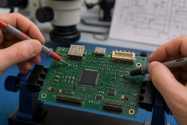
If the reading changes while the board is gently supported, suspect an intermittent trace, via barrel, solder joint, or connector contact. Apply movement only when the diagnostic procedure permits it, and never cut a trace, remove a component, or expose copper until the fault is reproduced and confirmed.
How Do You Check a PCB for an Unintended Short Circuit?
Start with two nets that the schematic says must be isolated. Disconnect external cables, compare the measured resistance with a known-good board of the same revision when available, and then isolate branches in a controlled sequence. The suspect area is the portion that remains connected after unrelated branches are removed.
- Inspect first: Look under magnification for solder bridges, conductive debris, damaged insulation, misaligned parts, and residue between adjacent pins. Map each visible suspect to the two measured nets so cosmetic residue is not mistaken for the electrical cause.
- Measure in resistance mode: Record the numerical value, probe polarity, and whether the reading rises, falls, or remains stable. A brief tone followed by increasing resistance suggests different behavior from a persistent value near the lead baseline.
- Separate branches: Disconnect external loads, connectors, or approved jumpers one at a time and retest after each controlled change. Record the original state and every removal so the branch that changes the reading can be identified and restored correctly.
- Compare locations: Probe multiple accessible points along both suspected nets to determine whether the low reading is local or present across the full network. A board-wide value may reflect a legitimate shared load; a change across one short section narrows the physical search.
Continuity locates an electrical relationship, not the physical defect by itself. Thermal methods, current-limited power injection, or component removal require a controlled repair procedure and are not substitutes for first confirming the unpowered resistance path.
Why Can a PCB Show Continuity When There Is No Short Circuit?
A continuity tone means the meter sees resistance below its audible threshold. It does not mean the path is zero ohms or that the board contains a short. The threshold, response speed, and test current vary by meter, so two instruments can behave differently on the same PCB.
Power and ground may beep because the circuit includes low-value loads, shunts, transformer windings, protection devices, or several parallel branches. Capacitors can also produce a brief tone while they charge from the meter. If the displayed resistance rises, the response is not the same as a stable metallic short.
Switch to resistance mode, observe the value over time, reverse the probes when semiconductor junctions may be involved, and compare the result with the schematic. A persistent low reading deserves investigation, but it must be judged against the design’s expected unpowered resistance. There is no universal resistance value that proves every PCB power rail is shorted.
An assembled circuit often contains several paths between the probe points. Treating it like a single copper trace creates false short and false open diagnoses.
- Capacitors: A discharged capacitor can produce a brief tone or low initial resistance that rises as it charges from the meter. Hold the probes steady and judge the settled value and repeatability instead of classifying the first beep as a short.
- Diodes and semiconductor junctions: A junction may conduct in one probe direction and block in the other, so continuity results can change when the leads are reversed. Compare both polarities and use diode mode when the schematic shows a semiconductor in the measured path.
- Inductors, fuses, shunts, and windings: These parts can be legitimate low-resistance series paths that trigger the tone. Confirm the component identity and expected resistance, then measure across the part and the surrounding copper separately to distinguish an open element from an open trace.
- Pull resistors and parallel networks: Parallel components can connect the endpoints through another branch even when the specific trace under test is open. Isolate an approved branch or move the probes to points that place only the target segment between them.
- Switches and connectors: The measured network changes with switch position, connector engagement, oxidation, and contact movement. Record the exact mechanical state and repeat the test without moving the probes before calling a changing value intermittent.
- Conformal coating and residue: Coating can prevent reliable metal contact, while conductive contamination can create a leakage path that looks like partial continuity. Use designated exposed test points, inspect the contact area, and clean only under an approved process before retesting.
When the reading is ambiguous, record it in resistance mode, reverse the probes, disconnect one approved branch at a time, and compare the time behavior. Those observations distinguish a fixed copper connection from a component-dependent path.
How Do You Test PCB Vias, Solder Joints, Connectors and Ground Connections?
Choose endpoints that place the feature itself in the measured path. A normal result means the connection matches the schematic and is close to the lead-resistance baseline when no intentional series element is present; an open, unstable, or unexpectedly low reading requires a nearer comparison point.
- PCB trace: Probe exposed nodes at both ends of the trace. A stable reading near the lead baseline is expected for a direct copper path; OL or instability points to a break, damaged pad, or poor contact.
- Via: Measure from an exposed pad before the layer transition to the nearest accessible point after it. An open result can indicate a cracked barrel or internal connection, although surface probing cannot show the exact internal failure location.
- Solder joint: Probe the component lead and the next copper node, not two points on the same solder fillet. A changing or high reading can indicate incomplete wetting, a crack, or a lifted pad.
- Connector: Test from the board-side net to the mating contact. The result should remain stable through the permitted engagement check; changes can indicate oxidation, weak contact force, or a damaged termination.
- Fuse: Probe one terminal on each side of the isolated fuse. A good low-resistance fuse should read near the lead baseline; OL indicates an open element or poor terminal contact.
- Ground connection: Confirm that both points belong to the same ground net before expecting continuity. Chassis, analog, digital, isolated, and filtered grounds may connect through controlled elements or remain separate.
Repeat an unexpected result from a second accessible point and inspect the feature before rework. Probe pressure can temporarily close a cracked joint or move a connector contact, producing a misleading pass.
How Is Continuity Testing Different on a Bare PCB and an Assembled PCBA?
An unpopulated PCB can be compared directly with its netlist because components do not create alternate paths. An assembled PCBA contains resistors, capacitors, inductors, semiconductors, connectors, and powered subsystems, so the same two test points may produce a legitimate reading that would look like a short on a bare board.
- Bare PCB objective: Verify that every required network is continuous and that separate networks remain isolated according to the released design data. A failure points toward copper, via, pad, or fabrication-data issues because installed components are not yet creating alternate paths.
- Assembled PCBA objective: Investigate one defined circuit relationship while accounting for components, jumpers, switches, connectors, and attached equipment. Before judging the reading, identify which installed paths can legitimately connect the selected points.
- Test coverage: A production bare-board program can check a controlled set of nets and isolation relationships systematically. A handheld PCBA check samples only the points chosen by the technician, so an untested branch cannot be called good from one passing pair.
- Acceptance basis: Bare-board acceptance can be tied to the released netlist and agreed electrical-test requirements. PCBA troubleshooting also needs the schematic, board state, component behavior, expected resistance or polarity, and a repeatable record of what was disconnected.
A bare-board pass does not prove assembly workmanship, component value, firmware operation, signal quality, or performance under load. Conversely, an unexpected assembled-board continuity reading does not prove that the bare PCB contains a fabrication defect.
When Is a Multimeter Continuity Test Not Enough?
A handheld meter is suitable for a small number of known points, but it does not provide complete network coverage or prove performance outside its low-energy resistance check. Escalate the test method when the decision depends on one of the following:
- High net count: Manually probing a few pairs cannot demonstrate systematic coverage on a dense board. Use a controlled test program derived from the released design data and retain the tested-net and exception record.
- Hidden structures: Surface probes cannot identify the physical condition of internal traces, buried vias, or bottom-terminated solder joints. Combine electrical localization with X-ray, cross-sectioning, or another inspection method selected for the suspected structure.
- Insulation requirements: A continuity function uses low test energy and cannot establish leakage or dielectric withstand at a specified voltage. Use the applicable insulation-resistance or high-potential method with defined limits and safety controls.
- Current-carrying risk: A thin or partially cracked conductor may pass the meter’s low-current check but develop excessive voltage drop or heating in service. Escalate to an approved resistance, voltage-drop, or loaded test when current capacity is the decision.
- Signal or functional risk: Continuity does not measure impedance, crosstalk, insertion loss, timing, firmware operation, component value, or performance under load. Use the powered functional or signal-integrity test that corresponds to the actual failure symptom.
- Intermittent reliability: A connection that passes at rest may fail only during thermal change, vibration, permitted flexure, or connector use. Reproduce the defined condition while monitoring the circuit with suitable logging instead of relying on a single static reading.
Choose the next method from the failure risk: resistance or diode mode for component-dependent readings, X-ray for hidden joints, insulation testing for leakage risk, powered measurements for operating behavior, and functional test for system outputs. Record the board revision, test points, circuit state, instrument, displayed value, and disposition so another technician can repeat the decision.
How Are PCB Opens and Shorts Tested During Manufacturing?
Production electrical testing compares the unpopulated board’s conductive networks with released design data. It checks required connections for opens and separate networks for unintended shorts under the agreed test conditions. The method is selected according to quantity, board access, program data, fixture economics, and reporting requirements.
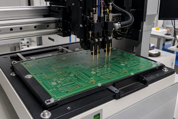
- Flying-probe test: Movable probes contact programmed pads without a dedicated bed-of-nails fixture, making program changes easier for prototypes and changing revisions. The quotation and test plan should state accessible-point limitations, expected coverage, program revision, and whether opens and shorts are both included.
- Fixture-based test: A dedicated fixture can contact many points simultaneously and shorten repeated test cycles after the design stabilizes. Before committing to it, confirm test-pad access, fixture ownership, maintenance, revision-change cost, and how engineering changes invalidate the fixture or program.
- Netlist control: The test program must represent the released board revision and the intended net relationships after any approved data transformation. Verify the source files, revision identifier, exclusions, and engineering-change linkage; a perfectly executed obsolete program can approve the wrong board.
- Result traceability: The retained record should identify the board or lot, program and design-data revisions, method, tested scope, pass/fail result, exceptions, retest disposition, and report-retention requirement. These fields let quality teams distinguish a real repeat failure from a changed design or test program.
Flying-probe testing often suits prototypes and changing revisions because it avoids a dedicated fixture. Stable mass-production volumes may justify a bed-of-nails fixture for shorter repeated test cycles. The choice does not change the acceptance basis: both methods need controlled netlist data, defined continuity and isolation criteria, and traceable results.
The scope of IPC-9252B electrical testing requirements addresses conductive networks on unpopulated printed boards. Electrical test does not replace dimensional and solder-mask inspection, assembly inspection, or functional testing.
A repeatable PCB continuity test record should identify the drawing, schematic, or netlist revision used for interpretation. Purchase documents should also state the governing requirement, supplied test data, reporting format, and project-specific limits.
FAQs About PCB Continuity Testing
Q1: Can I test PCB continuity with the power on?
A1: No. Continuity and resistance modes apply their own test stimulus, so external voltage can corrupt the reading and may damage the meter or board. Remove all power and verify the absence of voltage first.
Q2: What resistance should a good PCB trace have?
A2: A short direct copper path normally reads close to the meter’s lead resistance, but there is no universal value for every trace. Length, width, copper thickness, connectors, and intentional series elements affect the result.
Q3: Does a beep always mean continuity?
A3: It means the measured resistance is below that meter’s audible threshold. The path may be an intended trace, a component, a parallel branch, or an unintended connection, so the schematic determines its significance.
Q4: Why does my PCB beep between power and ground?
A4: Low-resistance loads, shunts, transformer windings, protection devices, parallel paths, or charging capacitors can connect the rails in an unpowered circuit. Read the resistance over time and compare it with the design before diagnosing a short.
Q5: Can a capacitor cause a continuity beep?
A5: Yes. The meter may briefly charge the capacitor, creating a tone or low initial resistance that rises. A stable low reading has a different diagnostic meaning.
Q6: Can a multimeter detect a broken via?
A6: It can show that the path across a via transition is open or unstable when accessible points exist on both sides. It cannot identify the precise internal crack location without layout data and additional inspection.
Q7: Does probe polarity affect continuity testing?
A7: It can on an assembled PCBA. Diodes, transistor junctions, and IC protection structures may conduct differently when the probes are reversed; diode mode can clarify the path.
Q8: Can continuity testing damage components?
A8: An energized circuit or an unsuitable meter test condition can create risk. Remove power, follow the component or product service guidance, and avoid probing modes that exceed the permitted terminal conditions.
Q9: Why does the continuity reading keep changing?
A9: Capacitor charging, unstable probe contact, connector movement, contamination, or an intermittent crack can change the effective path. Hold the probes steady, observe the time pattern, and isolate branches before assigning the fault.
Q10: Can a PCB pass continuity testing but still fail?
A10: Yes. A low-current path can pass while the board still has impedance, insulation, component, firmware, signal-integrity, current-capacity, or functional defects that continuity mode cannot evaluate.
A PCB continuity test is reliable when the circuit is unpowered, the expected net relationship is known, the meter and leads are checked, and the result is interpreted from resistance rather than a beep alone. Parallel paths, capacitors, semiconductors, contact quality, and mechanical movement must be considered before an open or short is assigned to the board.
If production continuity, isolation, or PCBA test coverage must be quoted, send the released Gerber or ODB++ data, netlist, BOM, quantity, test limits, and report requirements to sales@bestpcbs.com. EBest Circuit can review whether the requested scope belongs to bare-board electrical testing, assembly inspection, or project-specific functional testing.