In electronics, PWB stands for Printed Wiring Board. It refers to a bare board with conductive copper paths used to connect electronic components. Customers may also search for PWB board, although the wording is technically redundant because “board” is already included in PWB.
The term PWB is still used in engineering drawings, military documentation, aerospace specifications, and some older purchasing systems. In today’s commercial electronics industry, many buyers use PCB instead. However, when a project involves bare boards, component assembly, testing, or compliance documentation, the difference between PWB, PCB, PWA, PCBA, and CCA becomes important.
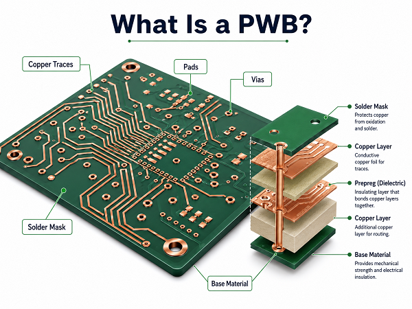
What Is PWB in Electronics?
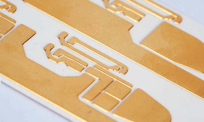
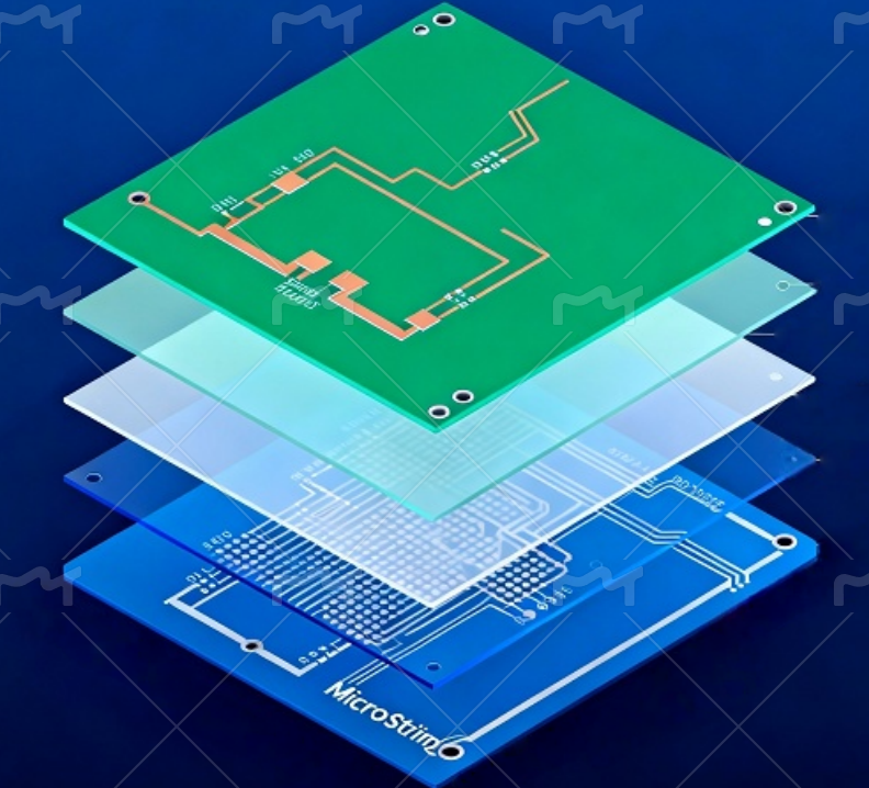
A PWB in electronics is a bare insulating board with copper traces, pads, vias, and sometimes surface finishes. Its job is to provide electrical wiring between components after those components are mounted.
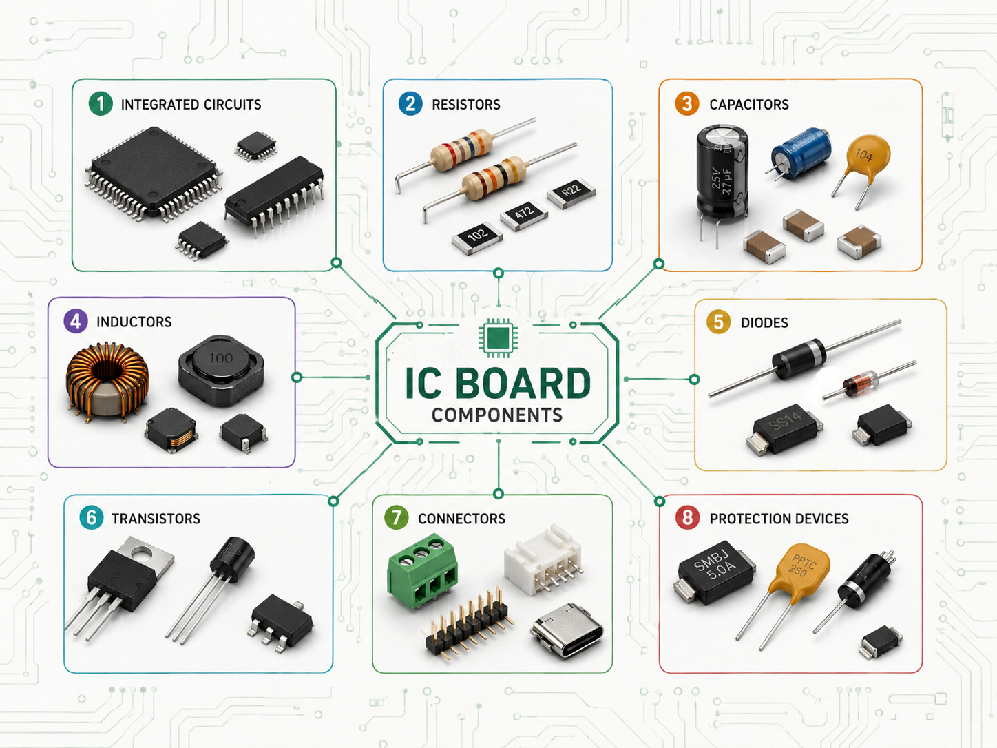
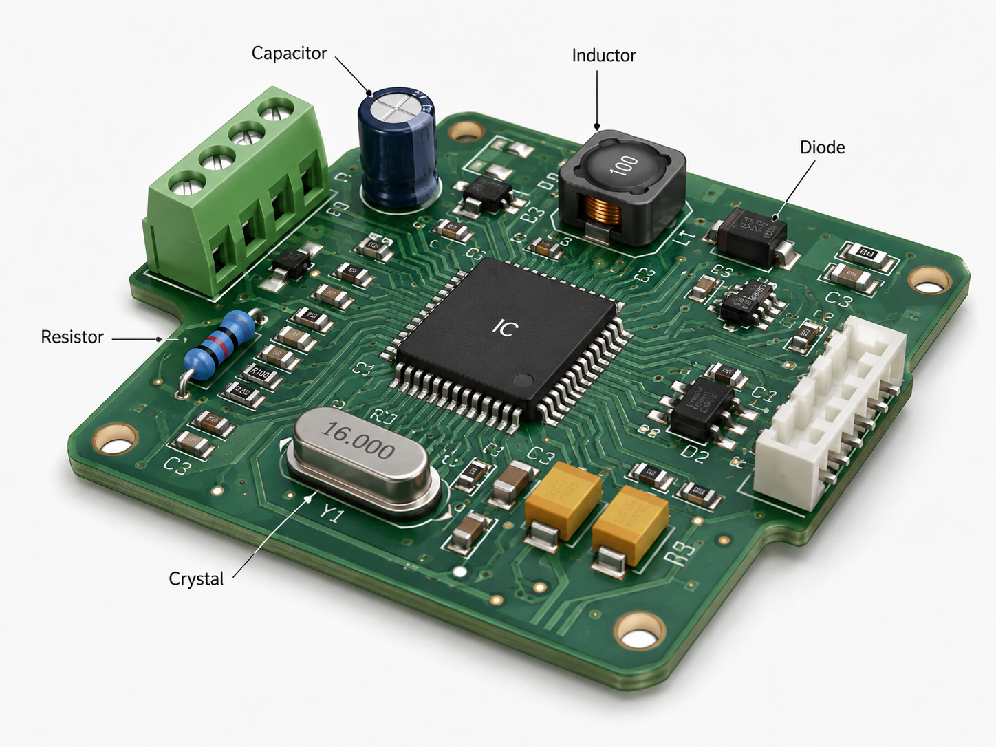
A typical PWB includes:
- Base material, such as FR4, polyimide, aluminum, ceramic, or high-frequency laminate
- Copper circuitry formed by etching or plating
- Pads for soldering components
- Vias for layer-to-layer connection
- Solder mask for insulation and protection
- Surface finish, such as HASL, ENIG, immersion silver, OSP, or hard gold
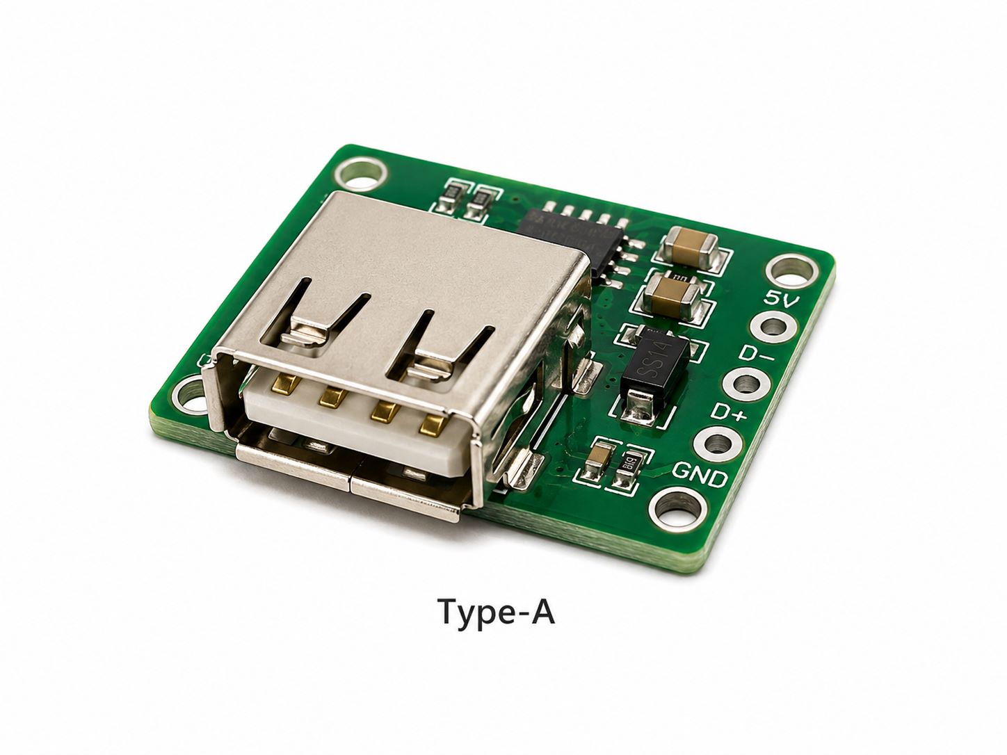
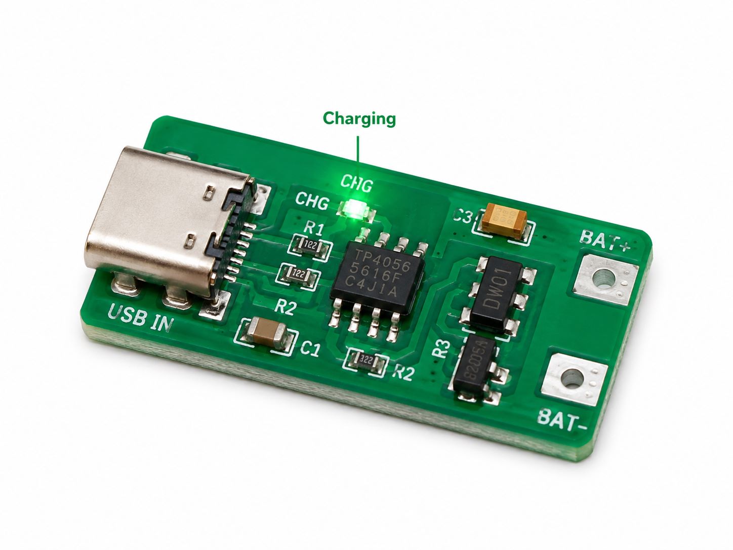
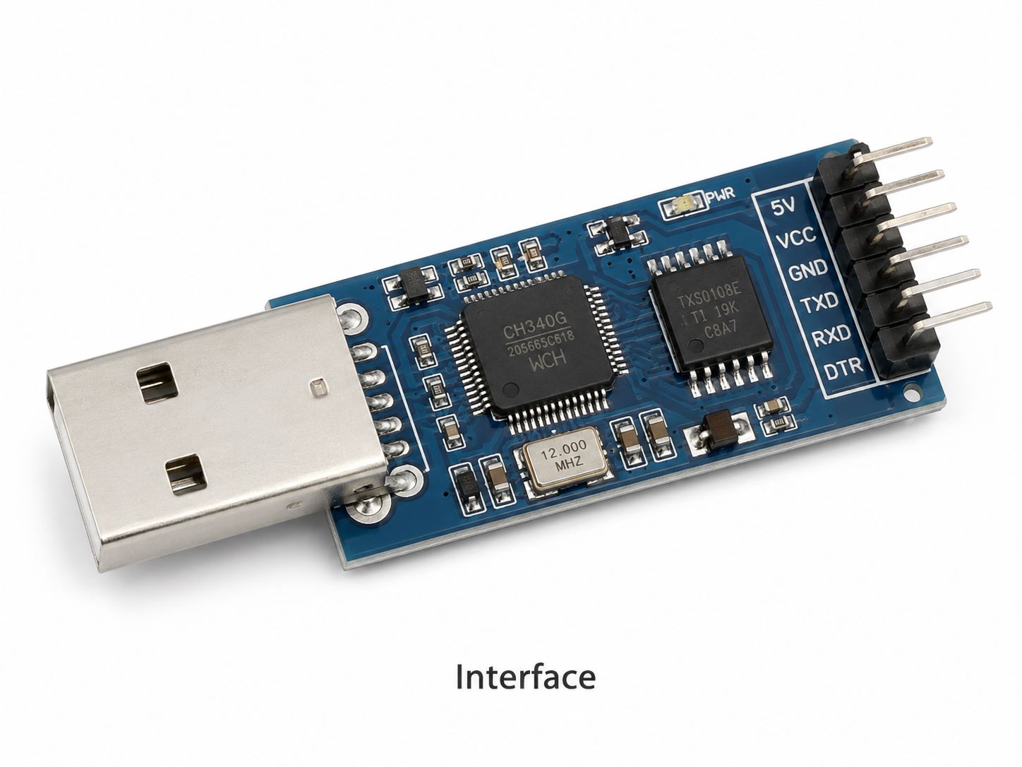
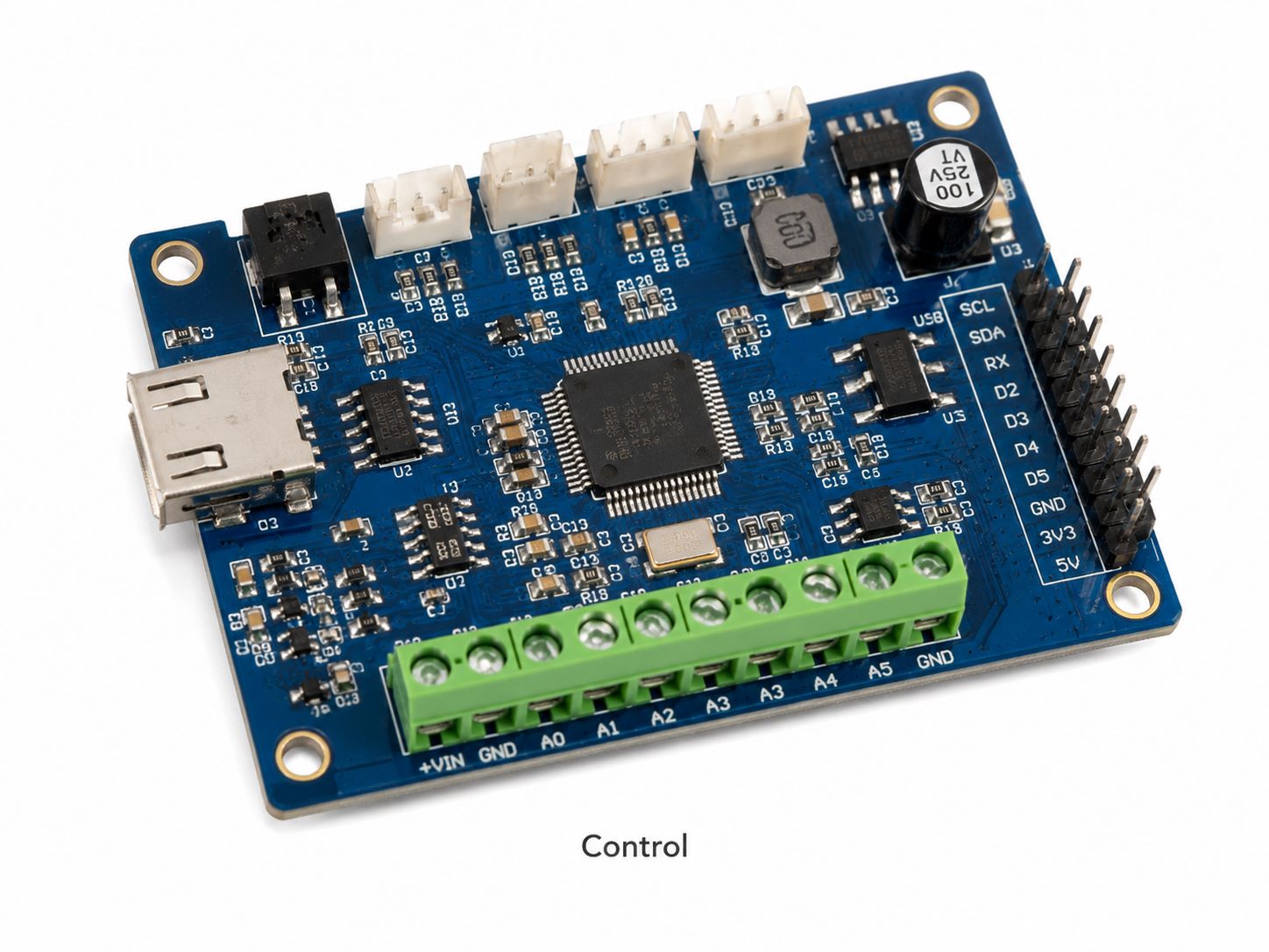
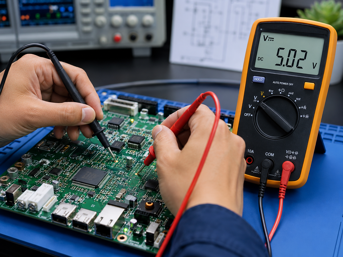
A PWB does not usually include installed components. Once resistors, ICs, connectors, capacitors, or mechanical hardware are assembled onto it, the product is normally called a PWA, PCBA, or CCA, depending on the industry and documentation standard.
What Are the Different Types of PWBs?
PWBs can be classified by structure, material, layer count, and application requirements. The right type depends on circuit density, current load, signal speed, temperature, mechanical space, and cost target.
| Type of PWB | Typical Structure | Common Use | Key Purchasing Consideration |
|---|---|---|---|
| Single-sided PWB | Copper on one side | Simple controls, LED products, low-cost electronics | Low cost, limited routing space |
| Double-sided PWB | Copper on both sides with vias | Power supplies, industrial controls, consumer devices | Good balance of cost and routing flexibility |
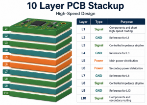
| Multilayer PWB | 4 or more copper layers | Communication, computing, automotive, medical devices | Requires stack-up control, impedance planning, lamination quality |
| Flexible PWB | Polyimide-based flexible circuit | Wearables, cameras, compact electronics | Bend radius, copper type, stiffener design |
| Rigid-flex PWB | Rigid and flexible sections combined | Aerospace, medical, compact modules | Higher cost, but reduces connectors and improves space efficiency |
| HDI PWB | Microvias and fine lines | Smartphones, high-density modules, IC-related designs | Laser drilling, via filling, fine-line control |
| Metal core PWB | Aluminum or copper base | LED lighting, power electronics | Thermal path, dielectric thermal conductivity, electrical isolation |
| High-frequency PWB | RF laminate or low-loss material | RF, radar, antenna, 5G modules | Dk/Df stability, impedance tolerance, material availability |
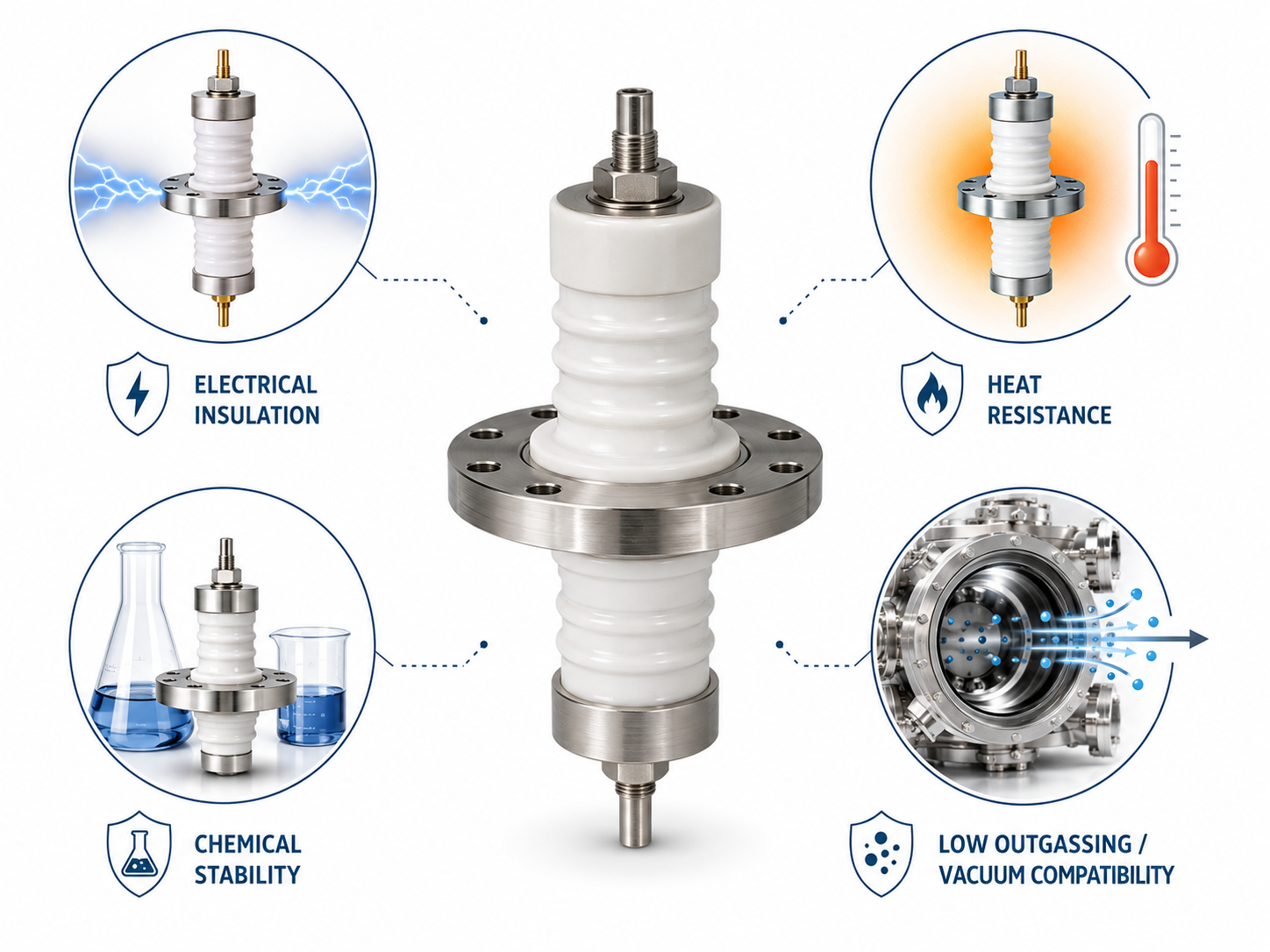
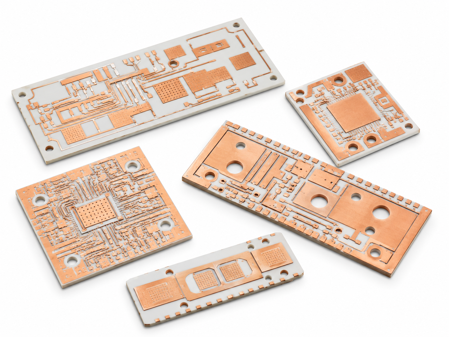
| Ceramic PWB | Alumina, AlN, or other ceramic substrate | High-power, high-temperature, laser, sensor applications | Thermal conductivity, metallization method, brittleness control |
For early prototypes, FR4 double-sided or multilayer boards are often enough. For high heat, RF performance, bending space, or high-density routing, the board type should be selected before layout is finalized, not after Gerber files are exported.
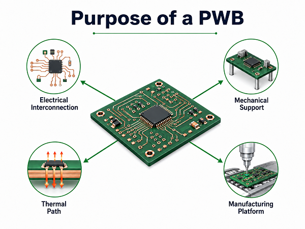
What Is the Purpose of a PWB?
The purpose of a PWB is to create a stable electrical and mechanical platform for an electronic circuit. It replaces loose wiring with fixed copper pathways, which improves repeatability, assembly efficiency, and product consistency. A PWB mainly serves 4 functions.
1. Electrical interconnection
Copper traces route power, ground, and signals between components according to the circuit design. For high-speed designs, trace width, spacing, dielectric thickness, and reference planes affect impedance and signal integrity.
2. Mechanical support
Components need a flat, stable base for soldering, handling, testing, and installation. Board thickness, panelization, copper balance, and material selection affect warpage and assembly yield.
3. Thermal management
Standard FR4 can handle many control circuits, but high-power LEDs, MOSFETs, power modules, and ceramic packages may require metal core PCB, heavy copper, thermal vias, or ceramic substrate.
4. Manufacturing repeatability
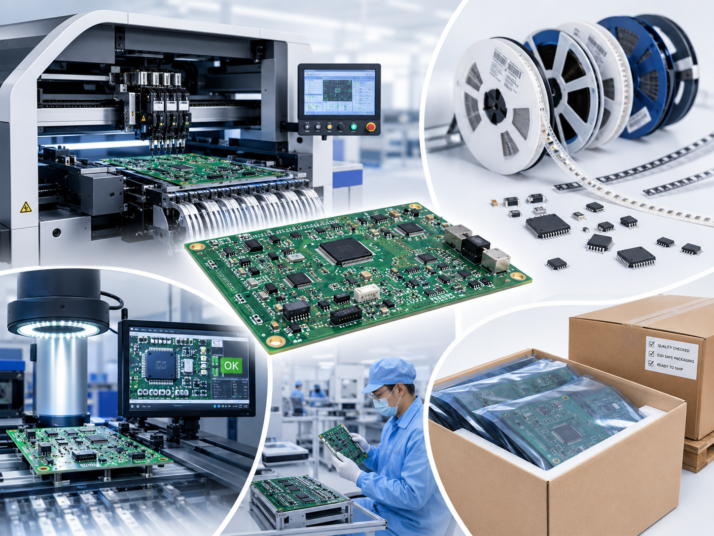
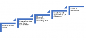
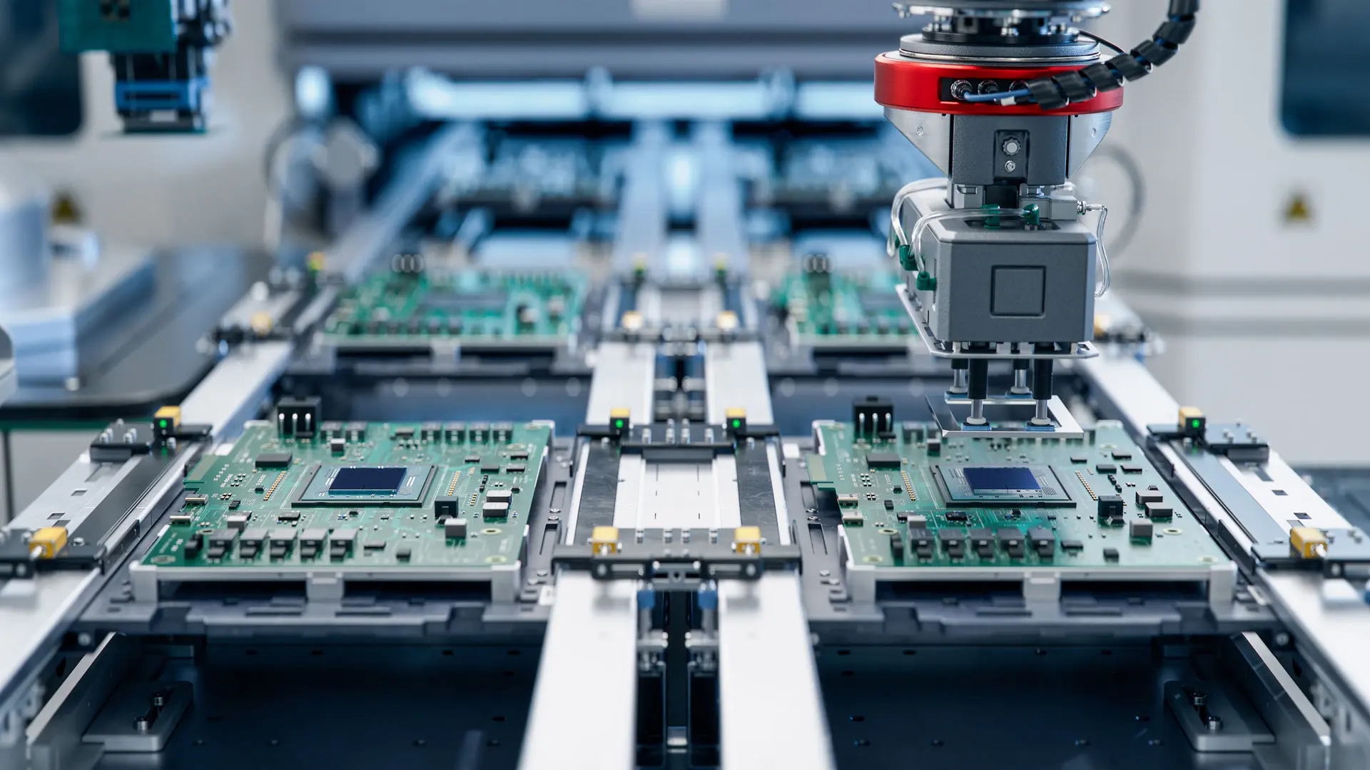
A well-designed PWB allows automated SMT assembly, AOI inspection, reflow soldering, functional testing, and batch production. This is why design files must match the intended production process.
What Are the Advantages of Using PWBs?
PWBs are used because they make electronic products more compact, repeatable, and manufacturable than hand-wired circuits.
Key advantages include:
- Stable electrical routing: Copper traces keep connections consistent across prototypes and production batches.
- Compact layout: Components can be placed closer together, which reduces product size.
- Better assembly efficiency: SMT and through-hole assembly can be automated.
- Improved reliability: Fixed copper paths reduce wiring errors, loose connections, and manual soldering variation.
- Design flexibility: Engineers can select different materials, copper weights, layer counts, surface finishes, and stack-ups.
- Scalable production: The same design can move from prototype to small batch and mass production with controlled documentation.
- Testability: Test points, fiducials, serial numbers, and inspection features can be added during layout.
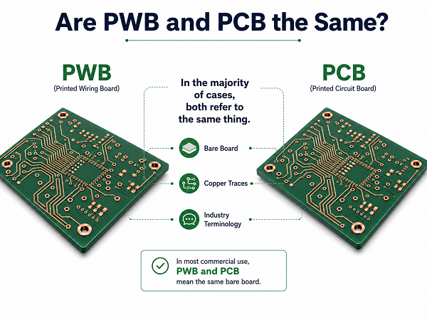
Are PWB and PCB the Same?
In many commercial conversations, PWB and PCB are used almost interchangeably. Both can refer to a bare board with printed copper circuitry. However, the wording can vary by industry, country, company, and documentation system.
The difference is mainly historical and contextual.
PWB emphasizes the board as a printed wiring structure. It was more common when the board was viewed as a replacement for point-to-point wiring.
PCB means Printed Circuit Board. It is now the more widely used term in commercial electronics. In most purchasing requests, PCB means the bare board before component assembly.
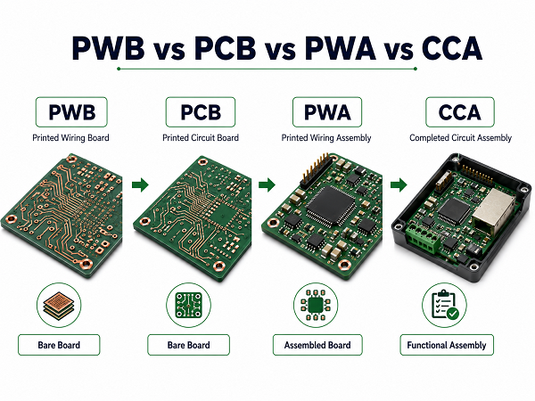
PWB vs PCB vs CCA: What Is the Difference?
The easiest way to understand PWB vs PCB vs CCA is to look at the production stage. PWB and PCB usually refer to the bare board. CCA refers to an assembled and functional circuit card.
| Term | Full Name | Production Stage | Includes Components? | Common Usage |
|---|---|---|---|---|
| PWB | Printed Wiring Board | Bare board | No | Aerospace, defense, older engineering documents |
| PCB | Printed Circuit Board | Usually bare board | Usually no | General electronics manufacturing |
| CCA | Circuit Card Assembly | Assembled board | Yes | Aerospace, defense, industrial systems, mission-critical electronics |
A CCA normally includes the board, soldered components, inspection, and sometimes conformal coating, programming, functional testing, or system-level validation. In regulated industries, CCA documentation may also include traceability, inspection records, material certificates, and special process control.
For customer purchasing, this distinction matters. If you send only Gerber files, the supplier can quote the bare PWB or PCB. If you want a CCA, you should also send BOM, pick-and-place data, assembly drawings, test requirements, coating requirements, and acceptance standards.
PWB vs PWA: What Is the Difference?
PWB vs PWA is a bare-board-versus-assembly comparison. A PWB is the printed wiring board before components are installed. A PWA, or Printed Wiring Assembly, is the PWB after electronic components have been mounted and soldered.
| Term | Meaning | What It Contains | Customer Files Usually Needed |
|---|---|---|---|
| PWB | Printed Wiring Board | Bare board only | Gerber, drill file, stack-up, material, finish, copper thickness |
| PWA | Printed Wiring Assembly | Bare board plus components | Gerber, BOM, pick-and-place file, assembly drawing, test instructions |
PWA is often used in technical drawings and quality documents. PCBA is more common in commercial manufacturing, but both terms refer to an assembled board.
When placing an order, avoid sending only “PWB board needed” if the project actually requires assembly. This can delay quotation because the supplier will still need BOM details, component sourcing preferences, and assembly standards.
PCB vs CCA: How Are They Different?
A PCB is usually the bare printed circuit board. A CCA is a populated and tested circuit card assembly. The difference affects cost, lead time, documentation, inspection, and supplier responsibility.
For a PCB order, the manufacturer is responsible for the board itself. This includes laminate selection, copper plating, solder mask, surface finish, dimensional tolerance, electrical test, and final inspection.
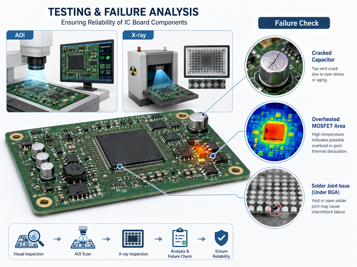
For a CCA order, the supplier must manage more variables. These include component sourcing, solder paste selection, SMT programming, through-hole assembly, X-ray inspection for BGA or QFN packages, cleaning, conformal coating, firmware loading, and functional testing when required.
| Comparison Point | PCB | CCA |
|---|---|---|
| Scope | Bare board fabrication | Board fabrication plus component assembly |
| Main files | Gerber, drill, stack-up | Gerber, BOM, pick-and-place, assembly drawing, test plan |
| Cost drivers | Material, layers, copper, finish, tolerance | PCB cost, components, assembly complexity, testing, yield control |
| Lead time drivers | Board complexity and quantity | PCB fabrication, component availability, SMT schedule, inspection |
| Supplier risk | Board quality | Board quality, component quality, assembly yield, functional result |
| Best for | Customers who assemble elsewhere | Customers needing a ready-to-test or ready-to-install module |
If your purchasing goal is a working electronic module, request CCA or PCBA quotation from the beginning. It gives the supplier enough information to evaluate component lifecycle, DFM risks, soldering process, and testing coverage.
Where Is PWB Commonly Used?
PWBs are used in almost every electronic product, but the board type varies by application. A low-cost consumer device and a high-reliability industrial controller may both use PWBs, but their materials, tolerances, testing, and acceptance standards can be very different.
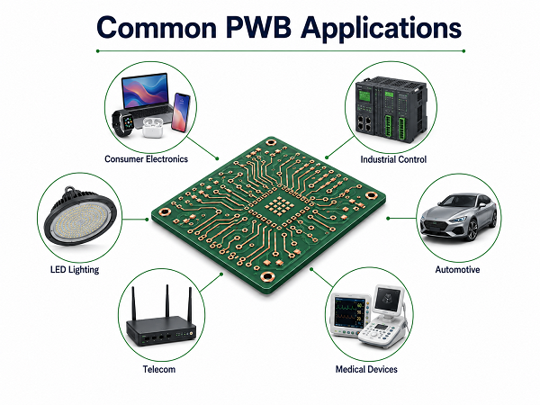
Common PWB applications include:
- Consumer electronics: Remote controls, chargers, smart home devices, audio products
- Industrial control: PLC modules, sensors, motor controllers, power monitoring boards
- Automotive electronics: Lighting, battery management, control units, charging modules
- Medical devices: Handheld instruments, diagnostic modules, monitoring equipment
- Telecommunications: RF modules, routers, base-station electronics, antenna systems
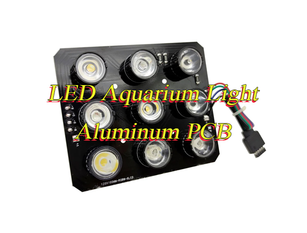
- LED lighting: Aluminum-based boards for heat dissipation
- Power electronics: Heavy copper boards, metal core boards, and high-current layouts
- Aerospace and defense: High-reliability PWBs, PWAs, and CCAs with strict documentation
- IoT and wearable devices: Flexible circuits, rigid-flex boards, compact multilayer designs
EBest Circuit (Best Technology) supports bare PCB/PWB fabrication as well as PCB assembly for customers who need prototype review, DFM feedback, material suggestions, and practical quotation guidance. This is useful when a customer is unsure whether the project should be quoted as a bare board, PCBA, PWA, or CCA.
FAQs
1. Is PWB board the same as PCB board?
In most commercial use, yes. PWB board and PCB board usually refer to the bare circuit board before assembly. Technically, “PWB board” and “PCB board” repeat the word “board,” but both phrases are widely understood by buyers and suppliers.
2. Is PWB still used as a term?
Yes. PWB is still seen in aerospace, defense, older technical documents, and some engineering drawings. PCB is more common in general electronics manufacturing.
3. When should I use PWB instead of PCB in a quotation?
Use the term shown in your drawing, customer specification, or industry standard. For most commercial suppliers, PCB is easier to understand. If your document says PWB, you can write “PWB/PCB bare board” to avoid confusion.
4. What files are needed for a PWB quote?
A basic PWB quote usually needs Gerber files, drill files, layer count, board thickness, copper thickness, material type, surface finish, solder mask color, quantity, and delivery requirement. For controlled impedance, provide impedance values and stack-up requirements.
5. What files are needed for a CCA quote?
A CCA quote needs more than bare board files. You should provide Gerber files, BOM, pick-and-place file, assembly drawing, test requirements, coating requirements, programming instructions if needed, and any approved vendor list for components.
6. Is a PCBA the same as a CCA?
They are closely related. PCBA means Printed Circuit Board Assembly and is common in commercial electronics. CCA means Circuit Card Assembly and is common in aerospace, defense, and high-reliability systems. CCA often implies stricter documentation, testing, and traceability.
7. Can one supplier handle PWB fabrication and assembly?
Yes. A one-stop supplier can fabricate the bare board and complete SMT or through-hole assembly. This can reduce communication gaps between board fabrication and assembly, especially when the design has tight spacing, BGAs, impedance control, heavy copper, or special materials.
8. How do I know whether I should order PWB, PCB, PWA, PCBA, or CCA?
Order PWB or PCB if you only need the bare board. Order PWA or PCBA if you need components assembled. Order CCA if you need an assembled board with higher documentation, inspection, testing, or system-level reliability requirements.
9. What should I check before sending a PWB project to production?
Check the material, copper thickness, minimum trace and spacing, via size, solder mask clearance, surface finish, impedance requirements, panelization, board outline, and assembly constraints. For high-power designs, also review current capacity and thermal path before production.
10. Can EBest Circuit help review whether my project needs PCB, PCBA, or CCA service?
Yes. If you provide the Gerber files, BOM, assembly files, application background, quantity, and testing expectations, EBest Circuit can help clarify whether your project should be quoted as a bare PCB/PWB, PCBA, PWA, or CCA.
Conclusion
PWB, PCB, PWA, PCBA, and CCA describe different stages of an electronic board project. PWB and PCB usually refer to the bare board. PWA and PCBA refer to assembled boards. CCA is often used when the assembled board requires stronger documentation, testing, or reliability control.
For customers, the practical decision is simple: define whether you need only the board, the board with components, or a fully tested assembly. Clear files and clear terminology help suppliers quote faster and reduce engineering back-and-forth. For PCB/PWB fabrication, PCBA, or CCA project support, you can contact EBest Circuit (Best Technology) at sales@bestpcbs.com.