Are you choosing a solder paste stencil and wondering which specifications matter most for SMT assembly? A solder paste stencil controls solder paste deposition on PCB pads, helping improve printing accuracy, solder joint consistency, and overall assembly quality.
This guide explains stencil materials, thickness options, design guidelines, printing methods, cleaning procedures, and service life. Whether for prototypes or volume production, understanding these fundamentals can help achieve more reliable SMT results.
What is Solder Paste Stencil?
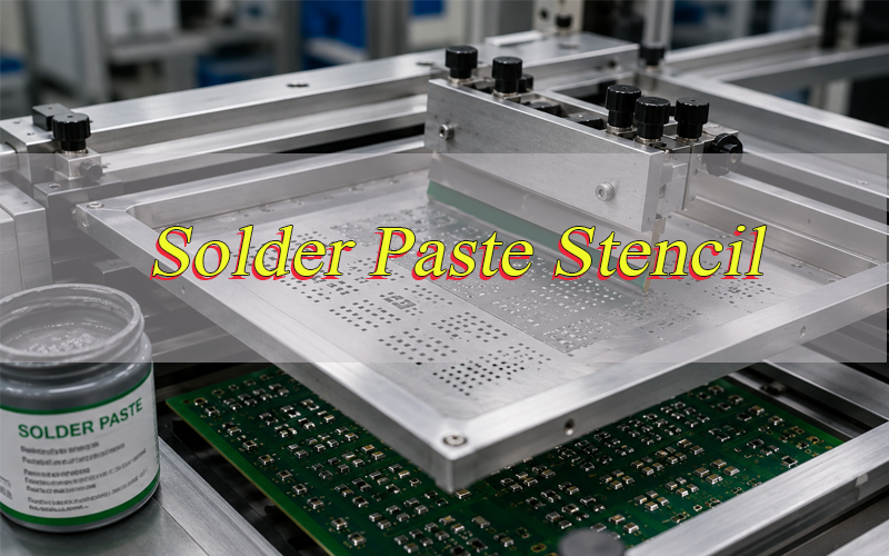
A solder paste stencil is a thin metal sheet with precisely cut openings that match the pad layout on a PCB. During SMT assembly, solder paste is printed through these openings onto specific locations before component placement.
Most stencils are manufactured from stainless steel using laser-cut technology. The openings determine how much solder paste is deposited on each pad, making stencil accuracy critical to assembly quality.
The stencil acts as a template between the PCB and the printing process. Without controlled solder deposition, issues such as solder bridging, insufficient solder, or poor solder joints may occur during reflow.
Because of its ability to deliver consistent solder volume and repeatable printing results, the stencil has become a standard tool in modern SMT manufacturing.
What is a Stencil Used for Solder Pasting?
The main purpose of a stencil is to transfer a controlled amount of solder paste onto PCB pads before component placement. Each aperture is designed according to the size and shape of the corresponding pad.
A stencil helps ensure that every solder joint receives a similar volume of paste. This consistency is important for achieving stable reflow results and reducing assembly defects.
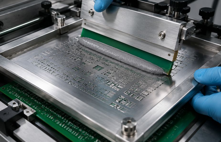
During printing, a squeegee pushes solder paste across the stencil surface. The paste fills the apertures and is transferred onto the PCB when the stencil separates from the board.
Compared with manual dispensing, stencil printing offers higher efficiency, better repeatability, and more uniform solder paste deposition, making it suitable for both prototypes and volume production.
What Materials Are Used for Solder Paste Stencils?
The most common materials used for solder paste stencils are stainless steel, electroformed nickel, and nano-coated stainless steel. Among them, stainless steel is the most widely used because it offers a good balance of durability, printing performance, and cost.
Stainless steel stencils are suitable for most SMT assembly applications and can withstand thousands of printing cycles. They are commonly used in both prototype and mass production.
For fine-pitch components and high-density PCB designs, electroformed nickel stencils provide smoother aperture walls and better solder paste release performance.
Some manufacturers also use nano-coated stencils, which reduce solder paste adhesion and improve cleaning efficiency during continuous production.
| Material | Main Advantage | Typical Use |
|---|---|---|
| Stainless Steel | Durable and economical | General SMT assembly |
| Electroformed Nickel | Better paste release | Fine-pitch devices |
| Nano-Coated Stencil | Cleaner printing | High-volume production |
What is the Thickness of Solder Paste Stencil?
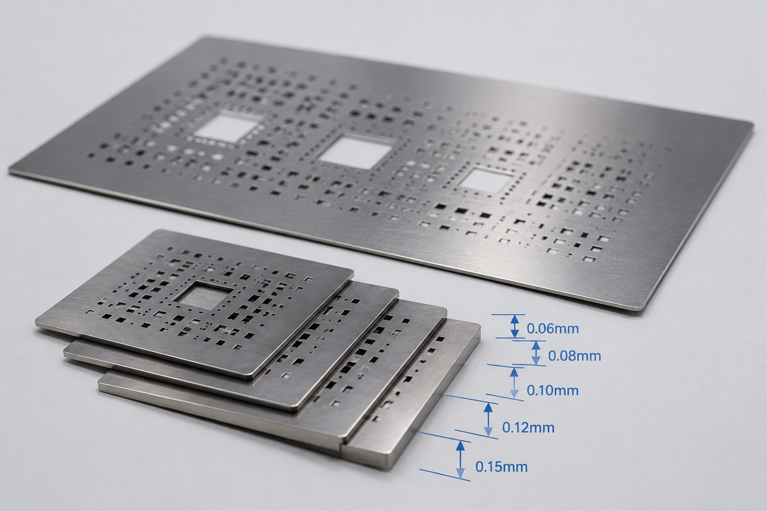
The standard solder paste stencil thickness is typically 0.08 mm, 0.10 mm, 0.12 mm, 0.15 mm, and 0.20 mm. For most SMT assemblies, 0.10 mm and 0.12 mm are the most commonly used options.
Thinner stencils are generally selected for fine-pitch components and high-density PCB layouts because they provide better control of solder paste volume and help reduce bridging.
Thicker stencils are often used for connectors, power devices, and components that require a larger amount of solder during assembly.
| Stencil Thickness | Typical Applications |
|---|---|
| 0.08 mm | 0201, 0402, fine-pitch ICs |
| 0.10 mm | Mixed SMT assemblies |
| 0.12 mm | Standard SMT production |
| 0.15 mm | Large components and connectors |
| 0.20 mm | High solder volume requirements |
Solder Paste Stencil Design Guidelines
Proper stencil design directly affects solder paste transfer, solder joint quality, and SMT production yield. A well-designed stencil helps achieve consistent printing results while reducing common assembly defects.
- Match stencil thickness to component size. Fine-pitch ICs and miniature components usually require thinner stencils, while connectors and power devices often need thicker stencils to provide sufficient solder volume.
- Optimize aperture size instead of copying pad dimensions exactly. In many cases, reducing the aperture slightly improves solder paste release and lowers the risk of solder bridging.
- Maintain a proper area ratio. The stencil area ratio affects how easily solder paste releases from the aperture. An area ratio greater than 0.66 is generally recommended for stable printing performance.
- Use window-pane openings for large thermal pads. Dividing a large aperture into multiple smaller openings helps distribute solder more evenly and reduces voiding during reflow.
- Modify apertures for fine-pitch components. BGAs, QFNs, and fine-pitch ICs may require reduced or specially shaped apertures to improve printing accuracy and minimize solder defects.
- Consider spacing between adjacent pads. Components with tight pad spacing are more prone to solder bridging, so aperture design should be adjusted accordingly.
- Ensure smooth aperture walls. Laser-cut and polished apertures improve solder paste release and help maintain consistent print quality over long production runs.
- Review manufacturing tolerances before fabrication. Verify aperture dimensions, pad alignment, and solder volume requirements to ensure the stencil can be manufactured accurately.
What Equipment Is Used for Solder Paste Stencil Printing?
Accurate solder paste printing requires several pieces of equipment working together. Each tool contributes to alignment accuracy, solder paste control, and process consistency.
- Stencil Printer – Aligns the PCB and stencil before printing. Automatic printers provide higher throughput and better consistency than manual systems.
- Squeegee Blade – Pushes solder paste across the stencil surface and fills the apertures. Blade pressure, speed, and angle directly affect print quality.
- PCB Support System – Uses support fixtures or vacuum platforms to keep the PCB flat during printing and prevent movement.
- Vision Alignment System – Uses cameras to align stencil apertures with PCB pads before printing begins.
- Solder Paste Inspection (SPI) System – Measures solder paste volume, height, and coverage to identify printing defects before component placement.
- Stencil Cleaning System – Removes residual solder paste from stencil surfaces and apertures, helping maintain stable printing performance.
How to Make a Solder Paste Stencil?
A solder paste stencil is usually manufactured from PCB Gerber files and serves as the foundation of the SMT printing process. A well-made stencil helps ensure accurate solder paste deposition, while a poorly designed stencil can lead to solder bridging, insufficient solder, or inconsistent printing results.
- Prepare the solder paste layer data. The stencil manufacturer uses the PCB solder paste layer to generate aperture openings. Before production, verify pad sizes, component spacing, and special package requirements.
- Optimize aperture openings. Apertures are often adjusted rather than copied directly from PCB pads. Small reductions can improve solder paste release and help prevent excess solder deposition.
- Choose the correct stencil thickness. Thickness should match component density and solder volume requirements. Fine-pitch assemblies generally require thinner stencils, while connectors and power devices may require thicker stencils.
- Laser cut the stencil. Laser cutting is the most widely used manufacturing method because it offers excellent dimensional accuracy and consistent aperture quality.
- Electropolish the apertures. Polishing smooths the aperture walls and improves solder paste release, especially for fine-pitch components.
- Perform final inspection. Aperture dimensions, stencil flatness, and overall quality should be verified before the stencil enters production.
How to Frame a Solder Paste Stencil?
Framing ensures that the stencil remains flat and properly tensioned during printing. Proper installation is important because even a small alignment error can affect solder paste deposition accuracy.
- Select the appropriate frame type. Framed stencils are commonly used for continuous production, while frameless stencils are often preferred for prototypes and small-volume orders.
- Inspect the stencil before installation. Check for scratches, bending, contamination, or other damage that may affect print quality.
- Mount the stencil evenly. Uniform tension across the stencil surface helps prevent distortion during printing.
- Verify alignment references. Fiducials and positioning marks should remain visible and accurately positioned after framing.
- Run a trial print. Testing before production helps identify alignment issues and confirms that solder paste deposits are forming correctly.
How to Apply Solder Paste with Stencil?
Stencil printing is the most common method used in SMT manufacturing because it provides fast, accurate, and repeatable solder paste deposition. Consistent printing is essential for achieving reliable solder joints during reflow.
- Secure the PCB firmly. The board should be supported properly to prevent movement during printing.
- Align the stencil accurately. Apertures must match PCB pads precisely to ensure solder paste is deposited in the correct locations.
- Apply the correct amount of solder paste. Too little paste can cause weak joints, while excessive paste increases the risk of bridging.
- Use proper squeegee settings. Squeegee pressure, speed, and angle should remain consistent throughout production.
- Separate the stencil smoothly. Careful separation helps maintain clean solder paste deposits and prevents smearing.
- Inspect the printed result. Check solder paste height, shape, and coverage before component placement.
How to Clean Solder Paste Stencil?
Cleaning is an important part of stencil maintenance. Residual solder paste left inside apertures can affect paste release and eventually lead to printing defects.
- Clean the stencil regularly during production. Frequent cleaning helps prevent aperture blockage and maintains stable print quality.
- Use compatible cleaning solutions. Cleaning chemicals should remove solder paste effectively without damaging the stencil surface.
- Pay special attention to fine-pitch apertures. Small openings are more likely to trap solder paste and require thorough cleaning.
- Inspect the stencil during maintenance. Cleaning provides an opportunity to identify scratches, wear, or damaged apertures.
- Store the stencil correctly after cleaning. Proper storage helps prevent contamination and mechanical damage.
What is Solder Paste Stencil Life?
A high-quality solder paste stencil can typically be used for thousands to tens of thousands of printing cycles under normal production conditions. The actual lifespan depends on stencil material, printing frequency, and maintenance practices.
Regular cleaning helps maintain solder paste release performance and extends stencil life. Residual solder paste inside apertures can affect printing accuracy and lead to inconsistent solder deposition.
Proper storage is also important. Stencils should be protected from bending, scratches, and contamination to maintain printing precision.
A stencil should be replaced when aperture wear, deformation, or poor paste release begins affecting print quality. A well-maintained stencil helps ensure consistent solder paste deposition and reliable SMT production results.
How to Apply Solder Paste without Stencil?
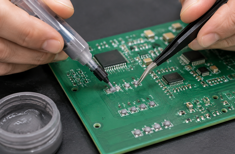
Although stencil printing is preferred for most SMT assemblies, manual solder paste application can be useful for prototypes, repairs, and very small production runs.
- Use a dispensing syringe. This is the most common alternative method and allows solder paste to be placed directly onto individual pads.
- Choose a suitable dispensing tip. Smaller tips provide better control when working with miniature components.
- Apply solder paste carefully. Excessive paste may cause solder bridging, while insufficient paste can affect solder joint strength.
- Inspect the paste deposits before assembly. Checking placement accuracy helps reduce defects during reflow.
- Reserve this method for low-volume work. Manual application is flexible but generally cannot match the consistency and efficiency of stencil printing.
For prototype projects, manual application can be effective, but for production quantities a stencil remains the most reliable solution.
FAQs About Solder Paste Stencils
Q1: What is the HS Code for Solder Paste Stencils?
A1: The HS code varies by country and customs regulations. Solder paste stencils are commonly classified as industrial metal templates or SMT manufacturing tools. Always confirm the exact code with your customs broker before shipment.
Q2: What is the Difference Between Framed and Frameless Stencils?
A2: Framed stencils include a fixed aluminum frame, while frameless stencils require a reusable mounting system. Framed stencils are preferred for production runs, while frameless stencils are more economical for prototypes and small batches.
Q3: Do I Need a Stencil for Solder Paste?
A3: No, but a stencil is the most accurate and efficient way to apply solder paste. Manual application is suitable for prototypes and repairs, while stencil printing provides better consistency and higher production efficiency.
Q4: Which Stencil Thickness Is Best for Fine-Pitch Components?
A4: A thickness of 0.08 mm to 0.10 mm is commonly used for fine-pitch components. Thinner stencils provide better control of solder volume and help reduce solder bridging.
Q5: When Should a Solder Paste Stencil Be Replaced?
A6: A stencil should be replaced when wear, damage, or poor paste release affects print quality. Replacing worn stencils helps maintain consistent solder deposition and SMT yield
Conclusion
A well-designed solder paste stencil helps ensure accurate solder paste deposition, reliable solder joints, and stable SMT assembly results. Choosing the right stencil specifications and maintaining proper printing practices can significantly improve production quality and efficiency.
If you are looking for a reliable SMT assembly partner, EBest PCB provides one-stop SMT services, including SMT stencil fabrication, component sourcing, SMT assembly, THT assembly, testing, and final product assembly. Whether you need prototypes or volume production, our team is ready to support your project with fast turnaround and dependable quality. Contact sales@bestpcbs.com today for a quotation.