The semi additive process is an advanced PCB fabrication method used to create fine copper traces for HDI boards, ultra-HDI boards, IC substrates, RF modules, and compact electronic devices.
Unlike subtractive etching, which removes unwanted copper from copper foil, this method builds copper only where the circuit pattern is needed. This supports finer line width, tighter spacing, cleaner trace profiles, and better dimensional control.
This guide explains what is semi additive process, how SAP works, where it is used, and how the semi-additive process vs subtractive etching comparison helps select the right circuit formation method for fine-line PCB projects.
What Is Semi Additive Process?
The semi additive process, often called SAP, is a PCB circuit formation method that combines copper plating with limited copper removal. It does not rely mainly on heavy copper etching.
SAP uses a thin seed copper layer as the base. Copper is then selectively plated onto the areas that will become traces, pads, and circuit features.
It is called “semi additive” because copper is added to the required circuit pattern, while only a thin seed layer is removed later. Compared with subtractive etching, this method can produce straighter trace walls, finer spacing, and better dimensional accuracy.
In PCB production, SAP is commonly used for HDI boards, ultra-HDI boards, advanced IC substrates, flexible circuits, and miniaturized electronics. It helps overcome the routing limits of conventional copper foil etching.
What Are the Main Steps of Semi Additive Process?
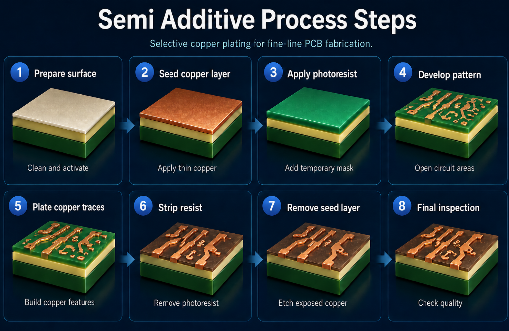
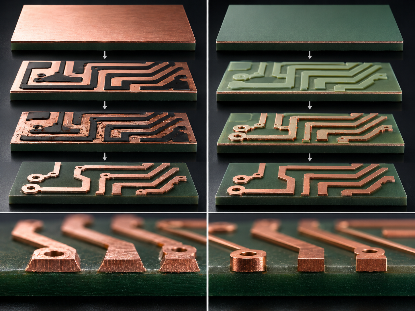
SAP forms PCB circuits by first creating a thin conductive seed layer. Copper is then selectively plated only where the circuit pattern is required. Compared with subtractive etching, this process removes much less copper. As a result, it can produce finer traces, cleaner line edges, and more stable spacing for advanced fine-line PCB manufacturing.
Step 1: Prepare the dielectric surface
The PCB substrate surface is cleaned and treated to improve copper bonding. This step removes contamination and prepares the surface for seed layer formation.
Step 2: Form a thin seed copper layer
A very thin conductive copper layer is applied to the surface. This seed layer provides the base for later electroplating.
Step 3: Apply photoresist
Photoresist is laminated or coated onto the panel. It works as a temporary mask during circuit pattern formation.
Step 4: Expose and develop the circuit pattern
The required circuit image is exposed onto the photoresist. After development, only the areas that need copper plating remain open.
Step 5: Electroplate copper traces
Copper is plated into the open pattern areas. These plated areas become the final traces, pads, and circuit features.
Step 6: Strip the photoresist
After copper plating, the remaining photoresist is removed from the panel. The plated copper circuit pattern is now exposed.
Step 7: Remove the exposed seed layer
The thin seed copper between traces is removed by flash etching. Because the seed layer is very thin, undercutting is much lower than in subtractive etching.
Step 8: Inspect the finished circuit layer
AOI, copper thickness measurement, adhesion testing, and microsection inspection are used to confirm line width, spacing, copper quality, and process stability.
What Is Modified Semi Additive Process?
The modified semi additive process, or mSAP, is a variation of SAP used in advanced PCB production. It is suitable when a circuit needs finer line width and spacing than standard subtractive etching can support.
In mSAP, production usually begins with thin copper foil or an ultra-thin copper layer. Copper is selectively plated to form the circuit pattern, and the exposed base copper is then removed.
This method reduces the amount of copper that needs to be etched. It helps create finer traces and more vertical trace profiles than traditional subtractive fabrication.
mSAP is widely used in smartphones, wearable devices, advanced modules, communication equipment, and compact PCB designs. It offers a balance between fine-line capability, production scalability, cost, and manufacturability.
What Is the Difference Between SAP and mSAP?
SAP and mSAP both use selective copper plating to form fine circuit patterns. The main difference is the starting copper layer, fine-line capability, cost, and production suitability.
| Item | SAP | mSAP |
|---|---|---|
| Full name | Semi Additive Process | Modified Semi Additive Process |
| Starting copper layer | Extremely thin seed copper layer | Thin copper foil or modified base copper |
| Main process logic | Build copper traces mainly by plating | Plate copper first, then remove thin base copper |
| Copper removal amount | Very low | Lower than subtractive etching, but higher than SAP |
| Fine-line capability | Better for ultra-fine lines | Suitable for many HDI fine-line designs |
| Typical line/space use | Ultra-HDI, IC substrate, advanced packaging | HDI PCB, compact modules, smartphones, RF boards |
| Trace profile | More rectangular and vertical | Near-vertical, depending on process control |
| Etching impact | Very small because seed copper is thin | Controlled, but still affected by base copper removal |
| Impedance stability | Stronger for very fine high-speed traces | Good for most HDI and high-density designs |
| Manufacturing difficulty | Higher | Medium to high |
| Cost level | Higher | More cost-effective for volume PCB projects |
| Production scalability | More demanding | Easier to scale in PCB production |
| Best application | IC substrates, ultra-HDI PCB, advanced miniaturized circuits | HDI PCB, RF modules, wearable devices, compact electronics |
| Selection point | Use when extreme line accuracy is required | Use when fine lines and cost control must be balanced |
For extremely fine traces and advanced packaging, SAP is usually stronger. For many HDI projects, mSAP provides a practical balance between performance, cost, and production efficiency.
How Is Semi Additive Process Different from Subtractive Etching?
SAP builds copper only where the circuit is needed. Subtractive etching removes unwanted copper from full copper foil. This difference directly affects trace accuracy, cost, and fine-line capability.
| Factor | Subtractive Etching | Semi Additive Process |
|---|---|---|
| Circuit formation method | Removes unwanted copper | Adds copper where traces are needed |
| Starting material | Standard copper-clad laminate | Dielectric surface with thin seed copper |
| Copper removal amount | High | Very low |
| Etching method | Main circuit formation step | Only used for seed layer removal |
| Trace edge control | Easier to form undercut | Cleaner and more controlled |
| Trace shape | More trapezoidal at fine pitch | More vertical and rectangular |
| Fine-line capability | Limited by etching accuracy | Better for fine-line and high-density circuits |
| Line width stability | More affected by etch factor | More stable after plating |
| Spacing control | Harder at very small gaps | Better for narrow spacing |
| Impedance consistency | Can vary due to trace profile | More stable for high-speed designs |
| Copper waste | Higher | Lower |
| Process cost | Lower for standard PCB | Higher for fine-line PCB |
| Design flexibility | Suitable for common PCB layouts | Better for dense routing and miniaturized designs |
| Typical PCB type | Standard PCB, conventional multilayer PCB | HDI PCB, ultra-HDI PCB, IC substrate, RF module |
| Best use case | Standard line width, cost-sensitive projects | Fine lines, tight spacing, dense BGA routing |
Why Does Semi-Additive Process Matter in Fine-Line PCB Manufacturing?
Fine-line PCB manufacturing needs stable trace width, tight spacing, controlled copper thickness, and reliable insulation between conductors. These factors directly affect yield, signal quality, and product reliability.
As electronic products become smaller and more powerful, more signals must be routed in limited board space. Standard subtractive etching may reach its process limit when trace geometry becomes too narrow.
SAP solves this issue by plating copper only in the required areas. This reduces lateral etching and keeps conductor dimensions more accurate.
This is important for HDI PCB, IC substrates, RF circuits, high-speed modules, medical electronics, and compact electronic systems.
Where Is Semi-Additive Process Used?
SAP is mainly used in fine-line, high-density, and miniaturized PCB applications where standard subtractive etching cannot provide enough routing space or trace accuracy.
Common applications include:
- HDI PCB
Used for dense routing, microvias, fine-pitch BGA breakout, and compact multilayer structures. - Ultra-HDI PCB
Suitable for extremely narrow line width and spacing, especially in advanced miniaturized electronics. - IC substrates
Used for high-density interconnection between chips, packages, and PCB systems. - RF and high-speed modules
Helps maintain stable trace geometry, impedance control, and signal performance. - Flexible and rigid-flex circuits
Supports compact interconnects in wearable devices, sensors, camera modules, and medical electronics. - Automotive electronics
Used in compact control modules, radar-related boards, sensor systems, and high-reliability electronic units. - Medical electronics
Suitable for small, precise, and reliable circuit boards used in monitoring, diagnostic, and portable medical devices. - Communication equipment
Applied in antenna modules, high-speed data modules, optical communication devices, and compact RF systems. - Consumer electronics
Common in smartphones, tablets, wearables, cameras, and other products requiring thin, dense, and lightweight PCB structures.
What Are the Advantages of Semi Additive Process?
The main value of SAP is better control over fine copper traces. It is especially useful when PCB layouts require narrow lines, tight spacing, and stable electrical performance.
Key advantages include:
- Finer line width and spacing
SAP can support fine-line circuits that are difficult to achieve with standard subtractive etching. - Cleaner trace profile
Since copper is plated where needed, the final trace shape is more vertical and consistent. - Lower undercut risk
Only the thin seed copper is removed during flash etching, so side etching is much lower. - Higher routing density
More traces can pass through limited PCB space, which helps reduce layout congestion. - Better impedance consistency
More stable trace width and profile help improve impedance control for high-speed and RF circuits. - Improved BGA breakout capability
This method helps route signals from fine-pitch BGA packages where standard etching may not provide enough space. - Lower copper waste
Less copper is removed compared with traditional subtractive etching. - Better support for HDI and ultra-HDI PCB
SAP is suitable for compact, dense, and high-performance circuit structures.
What Are the Limitations of Semi Additive Process?
SAP is powerful, but it is not necessary for every PCB project. It should be selected when fine-line capability, trace accuracy, and high-density routing justify the added process cost.
Main limitations include:
- Higher manufacturing cost
This process usually requires advanced equipment, tighter process control, and more inspection steps. - Stricter material requirements
The dielectric surface must support stable copper adhesion, dimensional stability, and reliable lamination. - Higher process sensitivity
Surface preparation, seed layer quality, imaging, plating, and flash etching must be tightly controlled. - More difficult plating control
Uneven copper plating can affect trace height, impedance, and fine-line yield. - Greater contamination risk
Small residues, particles, or resist scum can cause shorts, opens, or adhesion problems. - Not ideal for simple PCB layouts
Standard subtractive etching is usually more economical for normal line width and spacing. - Not always suitable for heavy copper designs
Wide power traces and thick copper layers may not benefit from SAP. - Requires early DFM review
Line width, spacing, copper thickness, stackup, solder mask, and inspection standards should be confirmed before production.
How Is Semi Additive Process Used in PCB Fabrication?
In PCB production, SAP is usually applied to layers that need very fine routing. A project does not always need this process on every layer.
Many advanced designs use a mixed manufacturing strategy. SAP or mSAP can be used for dense signal layers, while subtractive etching can remain on power layers, ground layers, or less dense routing areas.
This hybrid approach balances cost and performance. Dense layers benefit from fine-line capability, while standard layers remain more economical.
Before production, the stackup, dielectric thickness, copper thickness, target line width and spacing, via structure, impedance tolerance, and surface finish must be confirmed.
The manufacturer also needs to evaluate lamination, drilling, plating, solder mask registration, and final reliability testing.
SAP should be considered early in the project. If the layout is finished using ordinary subtractive assumptions, later conversion to SAP may require redesign.
What DFM Principles Change in Semi-Additive PCB Fabrication?
Semi-additive PCB fabrication needs tighter DFM control than standard subtractive etching. The key is to design according to real process capability, not only layout software limits.
- Minimum line width and spacing
Confirm the manufacturer’s stable production range before layout. Do not use the theoretical minimum as the mass production rule. - Copper thickness
Match copper thickness with trace width, impedance, and current requirement. Very narrow traces with excessive plated copper can reduce yield. - Trace profile
SAP traces are usually more vertical than etched traces. Use the manufacturer’s actual trace profile for impedance calculation. - Dielectric material
Confirm copper adhesion, dimensional stability, dielectric constant, and thermal performance. This is important for HDI, RF, and high-speed PCB projects. - Microvia structure
Check microvia diameter, depth, capture pad size, and registration tolerance. Poor microvia design can cause interconnection failure. - Solder mask clearance
Fine spacing requires tighter solder mask control. Review mask opening, bridge width, and registration tolerance before production. - Copper distribution
Uneven copper density can affect plating thickness. Balance copper distribution to improve plating uniformity across the panel. - Test coupons
Add impedance coupons, microsection coupons, and adhesion coupons. They help verify actual production quality. - Inspection standard
Define AOI, electrical test, copper thickness measurement, impedance test, and microsection requirements before fabrication. - Prototype validation
Validate fine lines, microvias, impedance, adhesion, and reliability before mass production.
What Quality Controls Are Needed for Semi Additive Process PCB?
Quality control for SAP boards should focus on trace accuracy, copper adhesion, plating quality, seed layer removal, and reliability.
AOI checks line width, spacing, trace edge quality, shorts, opens, nicks, and residual copper. Microsection analysis checks copper profile, via plating, and bonding quality.
For high-speed boards, impedance testing should be performed with controlled coupons. This confirms whether the actual process matches the design requirement.
Plating quality must be monitored closely. Uneven plating can cause trace height variation, rough edges, or local weak points.
Recommended quality controls include:
- AOI inspection for trace width, spacing, opens, and shorts.
- Microsection analysis for copper profile and via quality.
- Copper thickness measurement for plated trace consistency.
- Adhesion testing to verify copper-to-dielectric bonding.
- Impedance testing for high-speed and RF designs.
- Ionic contamination testing for reliability-sensitive products.
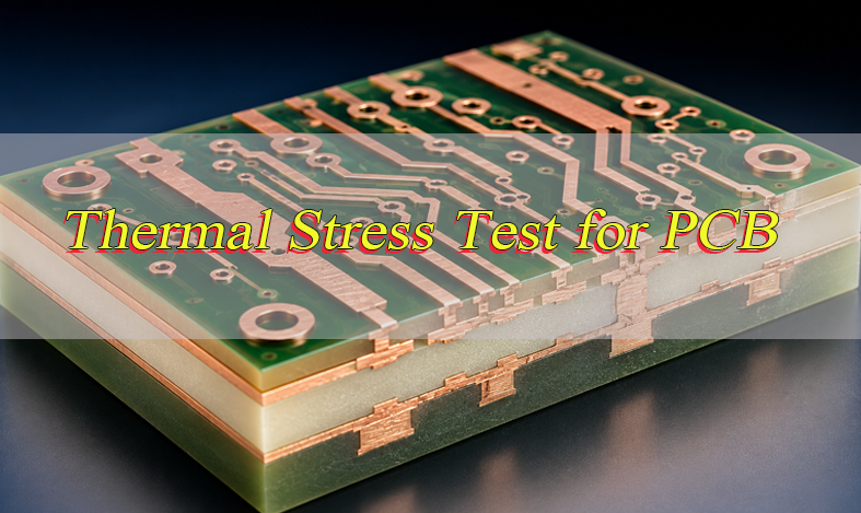
- Thermal stress testing for multilayer and HDI reliability.
- Solder mask alignment inspection for fine-pitch pads.
- Electrical testing for continuity and isolation.
- Process capability tracking for batch-to-batch stability.
Inspection standards, acceptance criteria, test coupons, and reliability requirements should be confirmed before mass production.
What Common Defects Should Be Avoided in Semi Additive Process PCB?
SAP defects usually come from poor surface treatment, unstable imaging, uneven plating, incomplete seed layer removal, or contamination.
- Open circuits
Caused by plating voids, resist defects, or over-etching. Control imaging, plating thickness, and AOI inspection. - Short circuits
Caused by residual seed copper, resist scum, or poor cleaning between fine traces. Control development and flash etching. - Poor copper adhesion
Caused by weak surface treatment or contamination. Improve cleaning, activation, material baking, and adhesion testing. - Trace width variation
Caused by uneven plating, exposure deviation, or poor process compensation. Monitor copper thickness and line width stability. - Residual seed copper
Caused by incomplete flash etching. It may lead to leakage or shorts between narrow traces. - Over-etching
Excessive flash etching can narrow traces and change impedance. Set a strict etching window. - Copper nodules
Usually caused by plating bath contamination or unstable chemistry. Use bath filtration and regular chemistry control. - Plating voids
Caused by poor activation, contamination, or unstable plating parameters. Use microsection inspection to verify plating quality. - Impedance drift
Caused by trace width variation, copper thickness change, or dielectric inconsistency. Use impedance coupons for verification. - Blistering or delamination
Caused by moisture, contamination, or poor bonding. Control material storage, baking, cleaning, and lamination. - Solder mask bridge failure
Caused by tight spacing and poor registration. Review solder mask clearance during DFM. - Microvia failure
Caused by weak via plating, poor capture pad design, or unreliable HDI stackup. Check microvia structure with microsection testing.
What Should You Confirm Before Starting a Semi Additive Process PCB Project?
Before starting a SAP project, confirm whether this process is truly required. If the design can be manufactured reliably with standard subtractive etching, SAP may add cost without enough value.
If the project requires ultra-fine routing, dense BGA breakout, or tight impedance control, SAP may be the better choice. The decision should be made before layout rules are finalized.
The first item to confirm is the target line width and spacing. The manufacturer should provide proven production capability, not only sample capability.
The second item is stackup feasibility. This includes dielectric thickness, copper thickness, via structure, lamination sequence, and impedance requirement.
Before releasing the project, confirm:
- Target line width and spacing.
- Copper thickness and trace height.
- Stackup and dielectric material.
- HDI structure and microvia design.
- Impedance requirements and tolerance.
- Surface finish, solder mask, and assembly needs.
- Prototype and mass production volume.
- Inspection standards and reliability tests.
- Cost target and acceptable process risk.
- File review and DFM feedback.
- Delivery schedule and quality documentation.
A successful SAP project depends on early technical alignment. Gerber files alone are not enough for advanced fine-line PCB manufacturing.
How to Choose a Reliable Semi Additive Process PCB Manufacturer?
Choosing a reliable SAP PCB manufacturer is not only about price. SAP and mSAP projects require fine-line capability, stable plating control, accurate inspection, and strong technical support.
- Check proven SAP or mSAP capability
Ask for the manufacturer’s stable line width and spacing range, not only the theoretical minimum. A reliable factory should know its real mass production limits for HDI PCB, ultra-HDI PCB, RF boards, and fine-line circuit layers. - Review fine-line production experience
The manufacturer should have experience with narrow traces, dense BGA breakout, microvias, impedance control, and advanced stackups. SAP defects often come from small process changes. - Confirm material and stackup support
A qualified supplier should help review dielectric material, copper thickness, resin system, build-up layers, via structure, and surface finish. Material compatibility affects copper adhesion, signal performance, and reliability. - Evaluate DFM support
The factory should provide DFM feedback before production. It should check line width, spacing, annular ring, solder mask clearance, microvia design, impedance structure, and manufacturing risk. - Check plating and flash etching control
SAP quality depends on copper plating uniformity and seed layer removal. Confirm control of plating thickness, bath chemistry, copper distribution, and flash etching window. - Confirm inspection and testing methods
Reliable SAP PCB production should include AOI, electrical testing, copper thickness measurement, microsection inspection, adhesion testing, and impedance testing when required. - Review prototype and mass production transition
The same process window, inspection standard, and material system should be controlled when moving from samples to batch orders. - Check quality documentation
Useful documents include inspection reports, impedance test results, microsection photos, copper thickness records, material certificates, and process traceability records. - Confirm technical communication efficiency
SAP projects often need discussion before production. Choose a supplier that can answer questions about stackup, tolerance, cost, lead time, risk points, and production feasibility. - Choose real manufacturing capability
A China-based source factory can be a practical option when it offers DFM review, OEM/ODM production, prototype support, mass production, strict quality control, and global delivery without false local claims.
FAQs About Semi-Additive Process
Q1: When should a PCB project consider SAP?
A1: SAP should be considered when standard etching cannot support the required line width, spacing, BGA breakout, or impedance stability. It is often used for HDI PCB, ultra-HDI PCB, IC substrates, RF modules, and compact electronic products with dense routing needs.
Q2: Can this process help reduce PCB layer count?
A2: In some designs, yes. Finer traces can provide more routing channels in limited space, which may reduce extra signal layers. This depends on component density, via structure, impedance rules, and stable production capability.
Q3: Is SAP suitable for prototype PCB orders?
A3: Yes, but prototype projects need detailed DFM review before production. Line width, spacing, copper thickness, material, microvias, impedance targets, and inspection requirements should be checked before cost and feasibility are confirmed.
Q4: What information is needed before requesting a quote?
A4: Gerber files, drill files, stackup, line width and spacing, copper thickness, material preference, impedance requirements, surface finish, quantity, delivery target, and inspection requirements are usually needed. For complex HDI projects, assembly files and reliability requirements are also useful.
Q5: Does SAP always mean higher PCB performance?
A5: Not always. SAP improves fine-line capability and trace geometry, but final PCB performance also depends on laminate material, stackup, copper thickness, impedance control, via reliability, surface finish, and assembly quality.
Q6: How does SAP affect high-speed signal design?
A6: SAP can improve conductor geometry and reduce trace width variation, which helps impedance consistency. For high-speed PCB designs, dielectric material, Dk/Df values, copper roughness, stackup thickness, and impedance coupon results should still be verified.
Q7: What makes SAP manufacturing harder than standard PCB fabrication?
A7: SAP requires tighter control of surface preparation, seed layer uniformity, imaging, copper plating, flash etching, and contamination. Small process changes can affect trace width, adhesion, impedance, and insulation between fine conductors.
Q8: How can real SAP capability be checked?
A8: Check proven line and spacing capability, sample records, process flow, inspection methods, microsection support, impedance testing, and mass production experience. A capable factory should provide DFM feedback before production.
Q9: Can SAP be used together with standard PCB processes?
A9: Yes. Some PCB designs use SAP or mSAP only on dense signal layers, while standard subtractive etching is used on power, ground, or less dense layers. This helps balance fine-line performance and manufacturing cost.
Q10: What risks appear when SAP design rules are too aggressive?
A10: Aggressive rules may cause low yield, trace width variation, short circuits, open circuits, impedance drift, poor adhesion, or higher scrap rate. Designs should use the factory’s stable production window, not only the minimum value shown in capability charts.
Summary
Choosing the right PCB fabrication process matters when a project requires fine lines, dense routing, stable impedance, and reliable long-term performance. If the design has reached the limits of traditional subtractive etching, SAP can provide better trace control, cleaner circuit geometry, and stronger support for HDI PCB, ultra-HDI PCB, RF modules, IC substrates, and compact electronic products.
If you are planning a fine-line PCB project, our team can help review stackup, line width and spacing, material selection, impedance requirements, prototype plan, and mass production feasibility. For OEM manufacturing, ODM production, sample development, mass production, or custom PCB solutions, contact us at sales@bestpcbs.com to get technical support and a quotation.