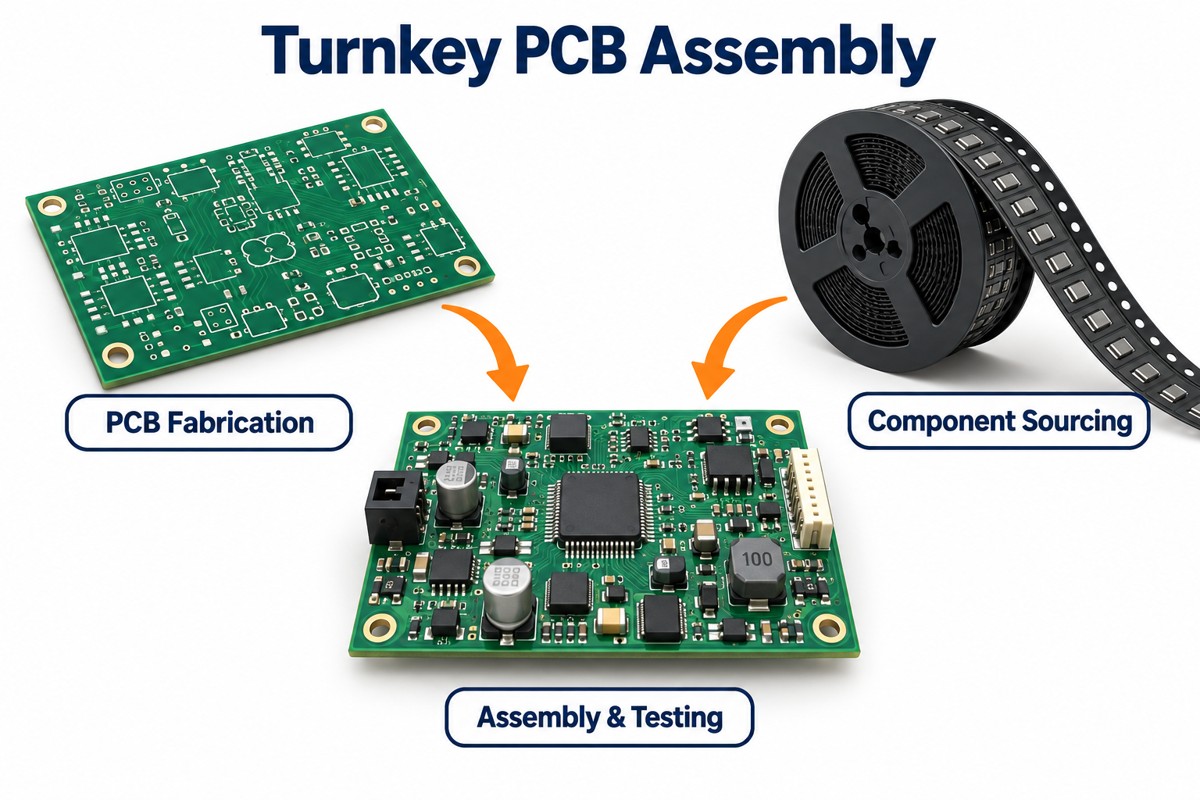
Turnkey PCB assembly combines bare-board fabrication, component procurement, assembly, and agreed inspection and testing in one managed order. At EBest Circuit, we coordinate these stages from your released design files, so your team does not have to separately manage a PCB fabricator, parts supplier, and assembly shop. We support SMT, through-hole, and mixed assemblies, from prototypes to production. Our engineering review checks whether the PCB data, BOM, component footprints, and assembly instructions agree before purchasing and production proceed. Send us your files, quantities, and test requirements for a project-specific quotation.
Key Takeaways
- Our turnkey PCB assembly services bring PCB fabrication, component sourcing, assembly, and agreed testing into one project.
- We support SMT, through-hole, and mixed assemblies. Standard FR-4 fabrication includes 1–10 layers, with high-Tg material required for 8 layers and above.
- Alternative components require your approval before they are introduced into the build.
- Our no-MOQ assembly service, DFM/DFA review, and online WIP updates support prototype builds and production planning.
- Our inspection equipment includes 3D SPI, 3D AOI, and X-ray. Functional testing needs a defined test procedure and acceptance limits.
- Price and delivery depend on the BOM, PCB construction, assembly complexity, quantity, and test scope.
- Send your Gerber files and BOM for a quotation, or share the files you have for an initial discussion if the design is still in progress.
What Does Our Turnkey PCB Assembly Service Include?
We can manage the bare PCB, purchased components, board assembly, and the inspection and testing agreed in your order. Our PCB assembly service can also include programming and additional integration work when specified in the quotation.
| Service stage | Our scope |
| PCB fabrication | FR-4 PCB, Multilayer PCB, HDI PCB, Heavy Copper PCB, Metal-Core PCB, Ceramic PCB, Flexible PCB, Rigid-Flex PCB, High-Frequency PCB, High-Tg PCB |
| Component sourcing | BOM Review, Authorized-Channel Procurement, Component Availability Checks, Alternative Part Proposals, Incoming Component Inspection, Customer-Supplied Parts Coordination |
| PCB assembly | SMT Assembly, Through-Hole Assembly, Mixed-Technology Assembly, BGA Assembly, Flex PCB Assembly, Ceramic PCB Assembly |
| Inspection and testing | First-Article Inspection, 3D SPI, AOI, X-Ray Inspection, Visual Inspection, Functional Testing |
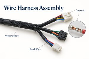
| Additional integration | Programming, Custom Wire Harnesses, Enclosure Assembly, Box Build Assembly, System Integration |
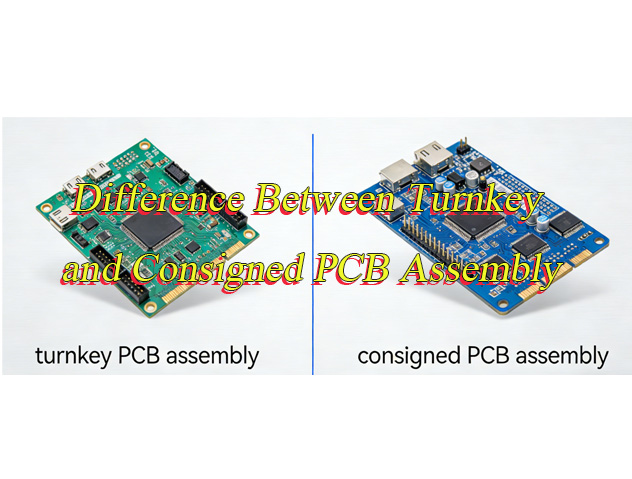
Full turnkey means we source the boards and components. In partial turnkey, you supply selected parts while we procure the remainder. Consigned assembly uses customer-supplied materials. We confirm responsibility for each item before the order is released, including extra components needed for setup and handling.
Why Choose EBest Circuit for Turnkey PCB Assembly?
Choose EBest Circuit when you need one team to coordinate PCB fabrication, component purchasing, and assembly decisions before production starts. We have provided PCB and PCBA services since 2006, supporting customers from engineering samples through repeat production.
- Resolve manufacturing questions before committing materials: we review the bare PCB and assembly requirements together. Footprint, panelization, and soldering questions can be addressed before boards are fabricated and components are purchased, helping avoid a board revision after materials have already been ordered.
- Keep control of component substitutions: our purchasing team checks authorized-channel availability and proposes alternatives when needed. Your engineers approve changes before use, so a purchasing decision does not silently change the circuit, footprint, or firmware requirements.
- Start with the quantity your design needs: our no-MOQ assembly service supports engineering samples without requiring a production-sized order. Setup, tooling, component pack sizes, and material minimum purchases remain visible in the quotation.
- Define how the build will be checked: we coordinate first-article inspection, SPI, AOI, X-ray, and the agreed functional tests. Your team can specify which measurements and records are needed for acceptance, rather than relying on an undefined claim that the boards are “tested.”
- Follow progress through one contact: online work-in-progress (WIP) updates and one-to-one sales support help you track production and resolve outstanding material or engineering questions without chasing separate suppliers.
- Extend the order beyond the PCBA: custom wire harnesses, enclosure assembly, and box build can be quoted with the board. This lets you define the wiring, programming, and final integration requirements in the same project.
For supplier qualification, our certification portfolio includes ISO 9001:2015, ISO 13485:2016, IATF 16949, and AS9100D. Request the current certificate and applicable manufacturing-site scope for your project.
Have a BOM shortage or an assembly question? Email the available files and your main concern to sales@bestpcbs.com. We can review component availability, manufacturing requirements, and the testing scope with you before you finalize the order.
As your turnkey PCB assembly manufacturer, we connect these services to a defined build: approved materials, released files, agreed inspection coverage, and a clear delivery scope. Our full turnkey PCB assembly overview explains the sourcing responsibilities when comparing full and partial turnkey orders.
Which PCB Types and Component Packages Can We Assemble?
We support SMT, through-hole, and mixed-technology assemblies, including boards with BGA devices. We review package geometry, board construction, and component temperature limits before confirming the process.
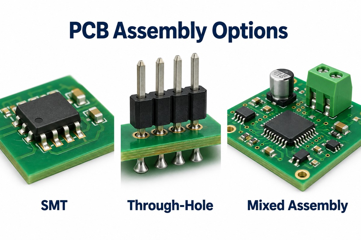
- SMT: surface-mount passives, ICs, and connectors are placed onto printed solder paste and reflowed.
- Through-hole: leaded connectors, relays, transformers, and other inserted components require a suitable soldering and inspection route.
- Mixed assembly: we plan the SMT and through-hole sequence together, accounting for component access and exposure to subsequent soldering operations.
- Flexible and specialty boards: support fixtures, thermal behavior, and handling requirements need review rather than assuming the same process as a rigid FR-4 board.
A package name alone is insufficient for approval. Include the exact manufacturer part number and package drawing, especially for bottom-terminated devices, fine-pitch connectors, and components with unusual mounting or thermal-pad requirements.
PCB fabrication capabilities supporting your PCBA: the values below distinguish our standard FR-4 process from special-process options. They describe bare-board fabrication, not guaranteed assembly limits.
| FR-4 parameter | Standard process | Special process, subject to engineering review |
| Layer count | 1–10 layers; high-Tg material for 8 layers and above | 10–32 layers |
| Inner-layer line width/spacing | 4/4 mil at 0.5 oz and 1 oz copper | 3/3 mil at 0.5 oz and 1 oz copper |
| Outer-layer line width/spacing | 4/4 mil at 1 oz copper | 3/3 mil at 1 oz copper |
| Minimum finished mechanical hole | 0.20 mm | 0.15 mm |
| Maximum through-hole aspect ratio | 8:1 | 10:1 |
Our standard high-Tg material options include ITEQ IT180, Shengyi S1000-2, and KB6167. Final material selection and routing limits depend on the specified copper weight, stack-up, dimensions, and fabrication requirements. Do not combine the smallest hole, finest trace, and highest layer count into one assumed process window.
Assembly and material-handling options:
- Reels, cut tape, tubes, trays, and loose components can be reviewed for the build. Packaging and supplied quantities affect feeder setup and handling.
- Our published fine-pitch capability includes 01005 components and 0.25 mm BGA pitch. These are advanced requests requiring engineering confirmation of the actual package, pad design, PCB construction, stencil, and inspection plan before order acceptance.
- We support FR-4, HDI, metal-core, ceramic, flexible, and rigid-flex PCB projects, with fixtures and soldering conditions selected for the substrate.
How Do We Manage Component Sourcing and BOM Changes?
We source against the approved BOM and ask you to confirm proposed alternatives before purchasing a substituted component. Our sourcing channels include component manufacturers and authorized distributors such as DigiKey, Mouser, Arrow, and Avnet.
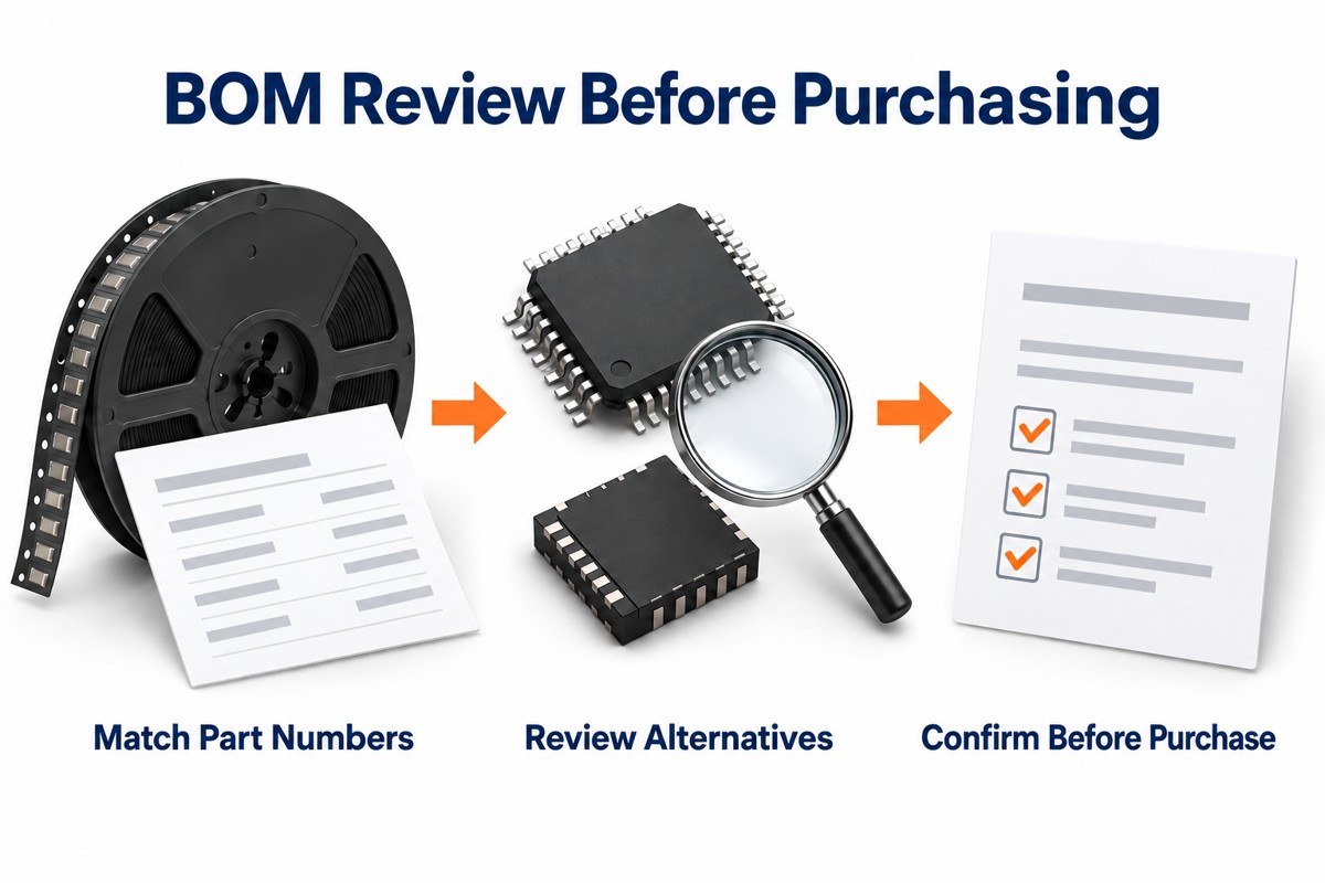
A purchasing-ready BOM identifies the manufacturer, full part number, quantity per board, reference designators, and any approved alternatives. Mark do-not-populate positions clearly. For customer-supplied components, identify the supplied quantities and packaging.
When a part is unavailable, our review should address more than its nominal value. A replacement resistor may differ in power rating or size; a connector may have a different mating interface; an IC may need firmware changes. We return the proposed substitution for engineering approval and use the approved BOM revision for the build.
What Do We Check Before PCB Assembly?
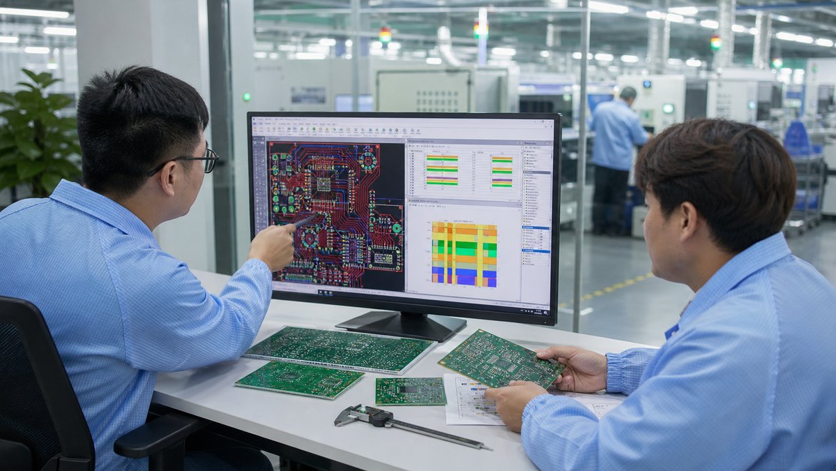
We check agreement between the fabrication files, BOM, placement data, and assembly drawing, then review the features that affect placement, soldering, inspection, and testing.
- Footprints and orientation: package dimensions, pin 1, diode and capacitor polarity, connector orientation, and reference designators.
- Board and panel details: fiducials, tooling features, component-to-edge clearance, breakaway areas, and handling support.
- Soldering details: stencil openings, thermal-pad paste coverage, solder-mask clearances, and components that need a special assembly sequence.
- Inspection and test access: visible joints, hidden joints requiring X-ray, programming headers, and accessible test points.
- Document consistency: matching PCB and BOM revisions, intentional unpopulated positions, and unambiguous assembly notes.
If the layout still needs work, our PCB design support can help address manufacturing questions before the release. DFM identifies production issues; it does not replace validation of the circuit’s electrical design.
How Does Our Turnkey PCB Assembly Process Work?
Our process moves from file review and quotation to material preparation, assembly, inspection, agreed testing, and shipment. Engineering questions and substitutions are resolved before the affected stage proceeds.
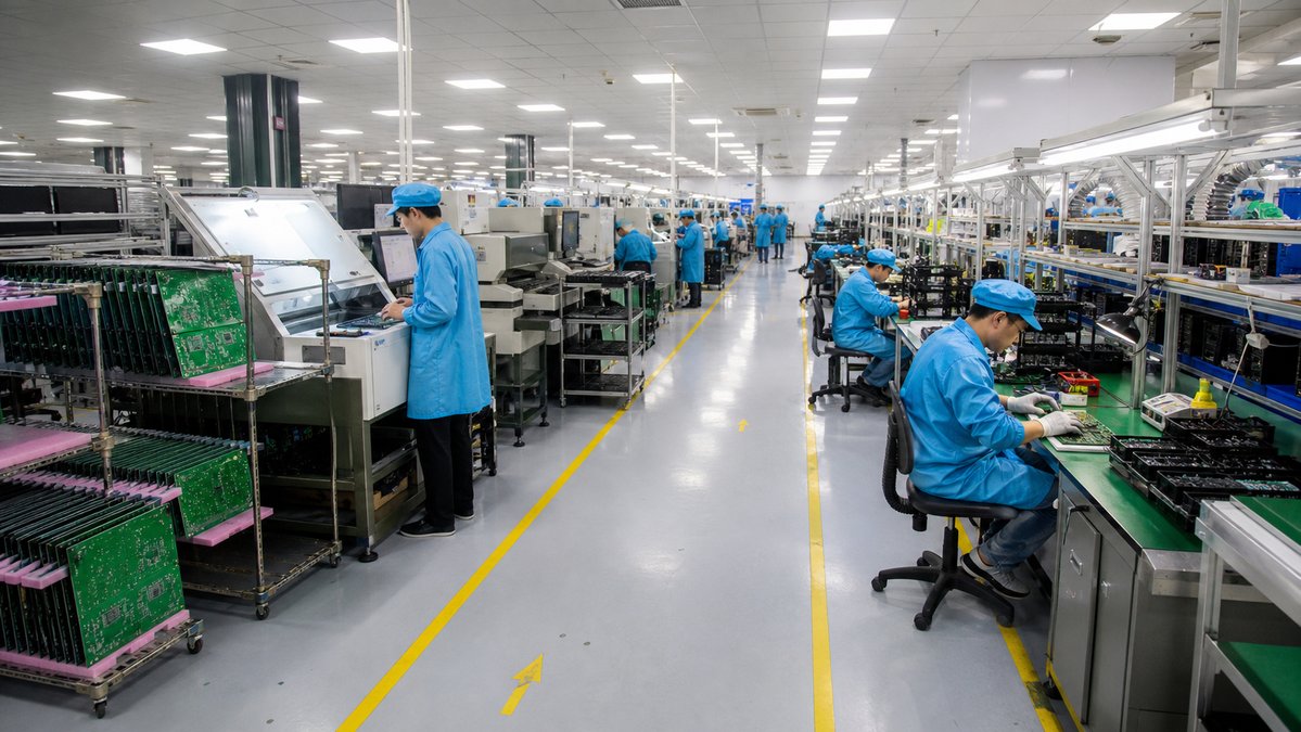
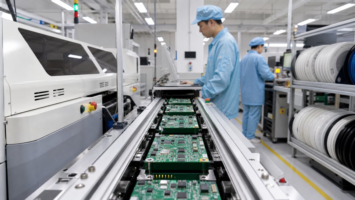
Our SMT equipment includes the GKG-GLS stencil printer, Yamaha YSM20R placement machine, and Suneast SER710NH nitrogen reflow oven. Nitrogen reflow provides a controlled soldering atmosphere for the selected process. Through-hole work can use the Suneast E-FLOW-610 wave soldering system where the board and component arrangement are suitable.
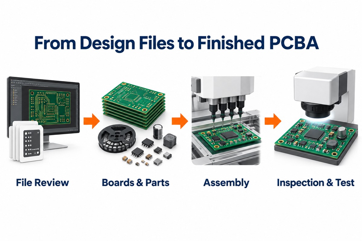
- Review your files: identify missing data, manufacturing questions, quantities, and test requirements.
- Confirm the quotation: agree on the PCB specification, procurement responsibility, assembly scope, schedule, and deliverables.
- Prepare boards and components: fabricate the PCB and procure the approved BOM, then check incoming materials against the order.
- Set up and assemble: prepare the stencil, placement program, soldering process, and first-article checks before continuing the batch.
- Inspect and test: apply the agreed process inspections, programming, and electrical or functional tests.
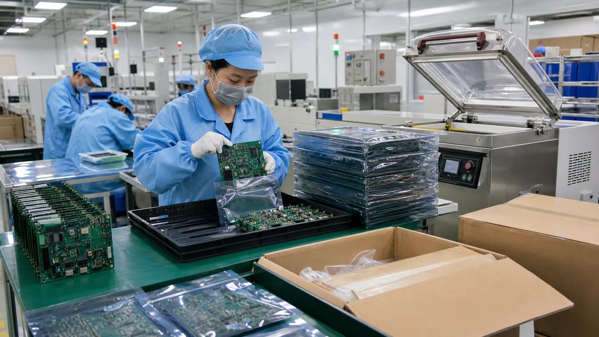
- Release and ship: complete the agreed records and packaging requirements for delivery.
This turnkey PCB manufacturing workflow allows procurement and fabrication to be coordinated, but the delivery date still depends on material availability and resolution of open technical questions.
How Do We Inspect and Test Your PCB Assemblies?
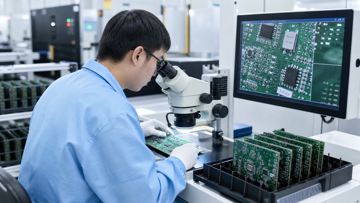
We use solder-paste inspection, optical inspection, and X-ray where applicable, then perform the electrical or functional testing defined for your project. Each method checks a different part of assembly quality.
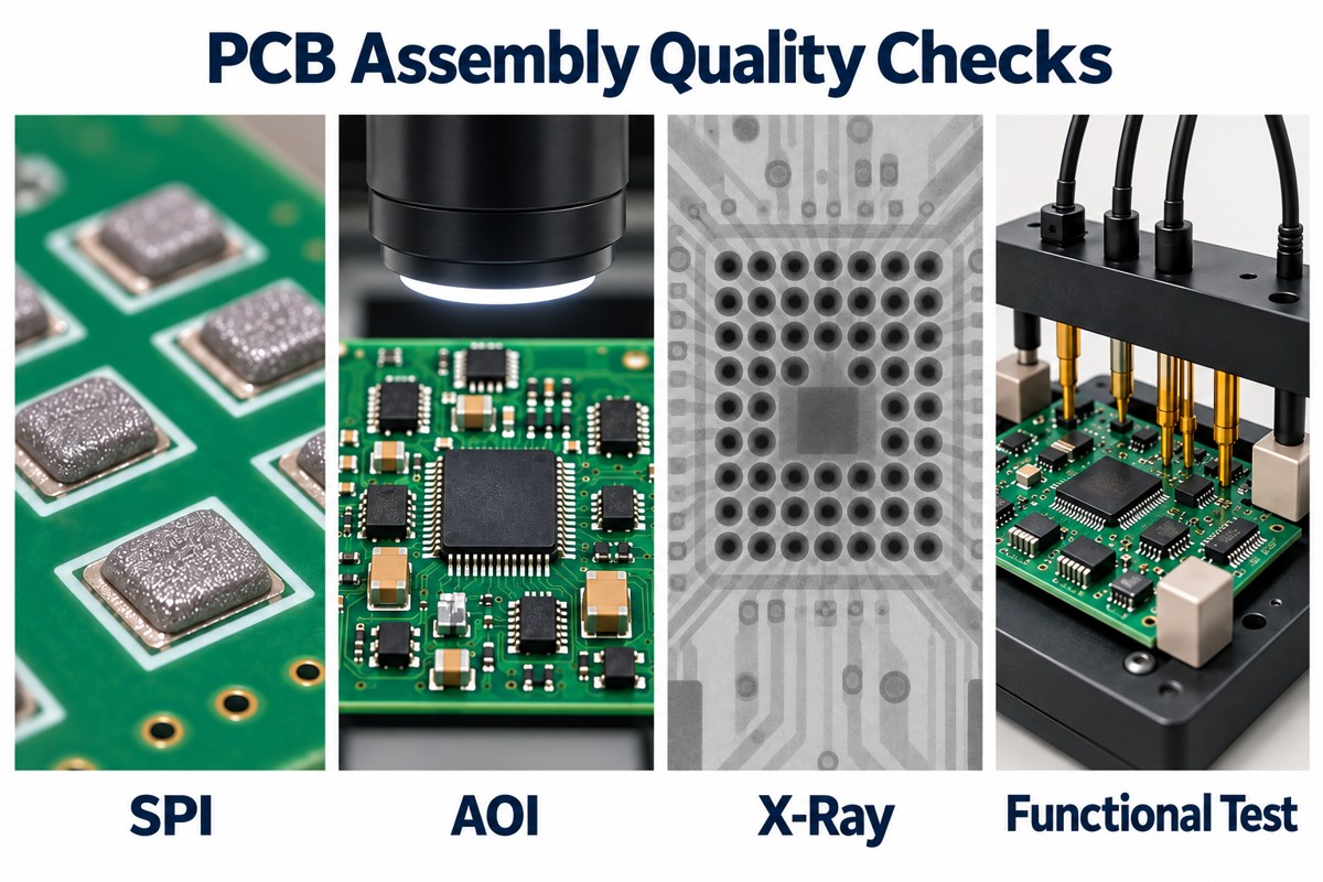
Our inspection equipment includes SINIC-TEK S8080 3D SPI, JCX830 first-article inspection, SINIC-TEK A510DL 3D AOI, and UNICOMP AX8200 X-ray. First-article checks verify the initial setup before the batch continues; SPI checks printed paste before placement, while AOI and X-ray address visible and hidden assembly features. This staged approach gives us opportunities to identify setup and soldering issues before final testing.
| Method | Primary check |
| 3D SPI | Solder-paste deposits after printing, including volume, height, and position. |
| AOI | Visible placement and soldering defects, such as missing components, misalignment, and visible bridges. |
| X-ray | Hidden solder-joint features, including selected BGA connections and voiding. |
| Electrical or functional test | Specified circuit behavior against agreed inputs, outputs, and pass/fail limits. |
An AOI or X-ray pass does not prove that the complete product functions correctly. For functional testing, provide the test procedure, supply conditions, firmware version, connections, and acceptance limits. Confirm whether fixtures, loads, programming equipment, or a known-good sample are needed during quotation.
For example, a power-control board may require checks of startup current, output voltage, and operation under a defined load. These limits must come from the product specification, not a generic assembly checklist.
Can We Support Both Prototypes and Production Orders?
Yes. We support no-MOQ prototype assembly, small batches, and production orders, with procurement and setup planned around the quantity and design maturity. Our PCB prototype service can support the bare-board stage of an assembled prototype project.
For a prototype, prioritize correct component selection, access for measurements, programming, and the tests needed to evaluate the design. Before a production repeat, release the final PCB files, BOM, assembly instructions, and firmware together. Tell us whether changes from the prototype affect the test fixture, component sourcing, or approved assembly process.
For repeat orders, we review current component availability and the released revision rather than assuming the previous purchasing conditions still apply.
What Determines Turnkey PCB Assembly Cost and Lead Time?
Cost is driven by the PCB specification, purchased components, assembly work, setup, inspection, and testing. Lead time is often constrained by the longest-lead component or a special PCB material, rather than placement time alone.
- PCB construction: layer count, material, copper weight, dimensions, surface finish, and special features.
- Components: exact part numbers, availability, order quantities, packaging, and approved sourcing channels.
- Assembly: placement count, double-sided processing, through-hole work, package complexity, and fixtures.
- Testing: programming, test development, fixtures, test duration, and required records.
- Order quantity: setup costs are spread across the batch, while component purchasing breaks can change the unit price.
To evaluate options, send a prototype quantity and expected production quantities together. We can quote the defined builds and discuss approved alternatives where sourcing is a constraint. We confirm delivery after reviewing files and current material availability; we will include the confirmed schedule in your quotation.
FAQ About Turnkey PCB Assembly
What is the turnkey PCB assembly meaning in a quotation?
It means the supplier manages the agreed board fabrication, component sourcing, and assembly scope. Check the quotation for testing, programming, shipping, and integration items, because these are not automatically identical across suppliers.
Can I supply an expensive or pre-programmed component?
Yes. A partial-turnkey order can combine your supplied components with parts we purchase. Confirm quantities, packaging, handling requirements, and responsibility for replacement parts before shipment.
Will you change an unavailable component without asking?
Proposed alternatives should be approved by your team before use. Provide an approved-vendor or alternative-part list when you want us to purchase from prequalified options.
Is box build automatically included?
No. Enclosures, cables, wiring, mechanical assembly, and system-level testing must be specified and quoted. A completed PCBA is not necessarily a finished enclosed product.
Can you quote before every design file is final?
We can review the available information for a preliminary quotation. Final pricing and production release require the agreed manufacturing files, BOM, quantity, and test scope.
Does a certified quality system make my product certified?
No. A manufacturer’s quality-system certification does not replace product-specific approvals or compliance testing. Tell us the documentation and product requirements that apply to your project.
Request a Turnkey PCB Assembly Quote from EBest Circuit
Send your Gerber files and BOM to sales@bestpcbs.com. We can review the PCB construction, component availability, assembly requirements, and testing scope, then prepare a quotation for the agreed build.
Ready for a quotation? Include the following where available:
- Gerber files and PCB fabrication specifications.
- BOM with manufacturer part numbers, quantities, reference designators, and approved alternatives.
- Pick-and-place data and assembly drawings.
- Prototype or production quantity, target delivery date, and customer-supplied components.
- Programming, testing, inspection-record, and box-build requirements.
Design still in progress? Send the files you have and tell us what needs to be resolved, such as a hard-to-source component, a fine-pitch package, or a prototype assembly requirement. You do not need a complete production package to start the discussion. Final pricing and production release will require the agreed files and specifications.
Our review will help identify missing information, procurement questions, and manufacturing or test requirements that affect the quotation. Tell us whether you need PCB fabrication and assembly only or a wider scope including programming, wire harnesses, and enclosure integration.