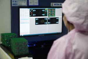
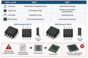
EBest Circuit is a one-stop PCB and PCBA manufacturing partner founded in 2006. We support bare PCB fabrication, component sourcing, SMT and through-hole assembly, testing, prototype builds, and volume production for global electronics projects.
If you are evaluating a PCB supplier for a new project, send us your Gerber files, BOM, stack-up, quantity, and testing requirements. Our engineering team can review the manufacturing package before quotation and help identify process risks early.
| Item | EBest Circuit Support |
| Core services | PCB fabrication, component sourcing, PCBA assembly, testing, box-build support |
| Project stage | Prototype, small-volume build, and volume production |
| Manufacturing support | Shenzhen, China and Vietnam manufacturing support |
| Technical review | DFM, stack-up, material, copper weight, impedance, assembly and test review |
| Typical files for review | Gerber, drill, stack-up, BOM, pick-and-place, drawings and test requirements |

Who Is EBest Circuit?
EBest Circuit is a PCB and PCBA manufacturing partner for electronics teams that need more than a bare-board supplier. We help customers move from early design review to PCB fabrication, component sourcing, assembly, inspection, and production planning.
Our work covers conventional rigid PCB projects as well as more specialized requirements such as HDI, RF/high-frequency materials, heavy copper, metal-core PCB, ceramic PCB, flexible PCB, rigid-flex PCB, and turnkey PCBA. For each project, we review the actual files instead of treating a single capability number as a universal answer.
What Can We Build?
We support both standard PCB technologies and project-specific builds that require engineering review. The best starting point is a complete manufacturing package, because layer count, material, copper weight, hole structure, board size, surface finish, assembly requirements, and testing all affect feasibility.
| Product or Service | Typical Support |
| Rigid PCB | Single-sided, double-sided and multilayer rigid PCB fabrication |
| HDI PCB | Fine features, laser blind/buried vias and high-density interconnect structures |
| RF / High-Frequency PCB | Rogers, Taconic, PTFE, Isola, Nelco and other specified laminates |
| Heavy Copper PCB | High-current and mixed-copper designs reviewed by stack-up and copper distribution |
| Metal-Core PCB | Aluminum, copper and stainless-steel substrate options |
| Ceramic PCB | Thin Film, DBC/DCB, DPC and AMB ceramic substrate technologies |
| Flexible PCB | Single-, double- and multilayer FPC through our flexible PCB support path |
| Rigid-Flex PCB | Combined rigid and flexible structures for compact electronic assemblies |
| PCB Assembly | SMT, THT/DIP, mixed assembly, component sourcing and agreed testing |
| Box-Build Support | PCB with cable, wire, enclosure or project-specific assembly requirements |
For flexible PCB and rigid-flex projects, customers can also review our dedicated flexible PCB manufacturing resources at bestfpc.com. For ceramic substrate projects, our ceramic PCB information is available at bstceramicpcb.com.
How Do We Review PCB Manufacturing Capability?
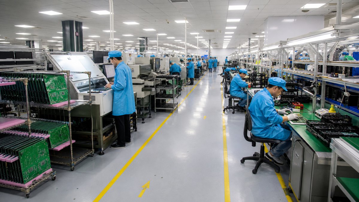
PCB capability depends on the full construction, not only on one headline parameter. A 32-layer rigid PCB, a 20 oz heavy copper board, a 0.10 mm laser via design, and a special laminate project may each require a different review path.
Our current FR-4 process specification separates standard process ranges from special-process review. The table below summarizes key items customers often ask about during supplier evaluation.
| Capability | Standard Process | Special Process / Review |
| FR-4 layer count | 1-10 layers | 10-32 layers |
| Inner copper | 0.5-5 oz | 5-20 oz |
| Outer copper | 1-5 oz | 5-20 oz |
| Laser blind/buried via | 0.10 mm | Project construction must be reviewed |
| Minimum finished mechanical hole | 0.20 mm | 0.15 mm |
| Through-hole aspect ratio | Up to 8:1 | Up to 10:1 |
| Inner trace/space | 4/4 mil at suitable copper | 3/3 mil at suitable copper |
| Outer trace/space | 4/4 mil at suitable copper | 3/3 mil at suitable copper |
| Surface finishes | OSP, HASL, ENIG, ENEPIG, immersion silver, immersion tin, hard gold and others | Project dependent |
These values should be used as an early screening reference. Final manufacturability still depends on the complete stack-up, panel size, copper distribution, finished thickness, tolerance, surface finish, quantity, and inspection requirements.
Why Do Engineers Work With Us?
Engineering teams work with us because many PCB problems are easier to solve before production starts. We review the design package early so customers can correct unclear specifications, high-risk stack-ups, component sourcing gaps, or testing assumptions before they become schedule and reliability problems.
- Gerber and drill-file completeness review.
- Stack-up, material and finished thickness review.
- Copper weight, spacing and impedance discussion.
- Hole, via, blind/buried via and HDI structure review.
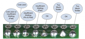
- Surface finish and solderability review.
- BOM sourcing and component availability checks.
- SMT, THT/DIP and mixed-assembly process review.
- Inspection and functional-test planning.
- Prototype-to-production transition support.
This approach is especially useful for HDI, RF PCB, heavy copper PCB, metal-core PCB, ceramic PCB, rigid-flex PCB, dense PCBA, BGA assembly, fine-pitch components and projects with formal inspection documentation.
How Do We Support PCB Materials and Special Technologies?
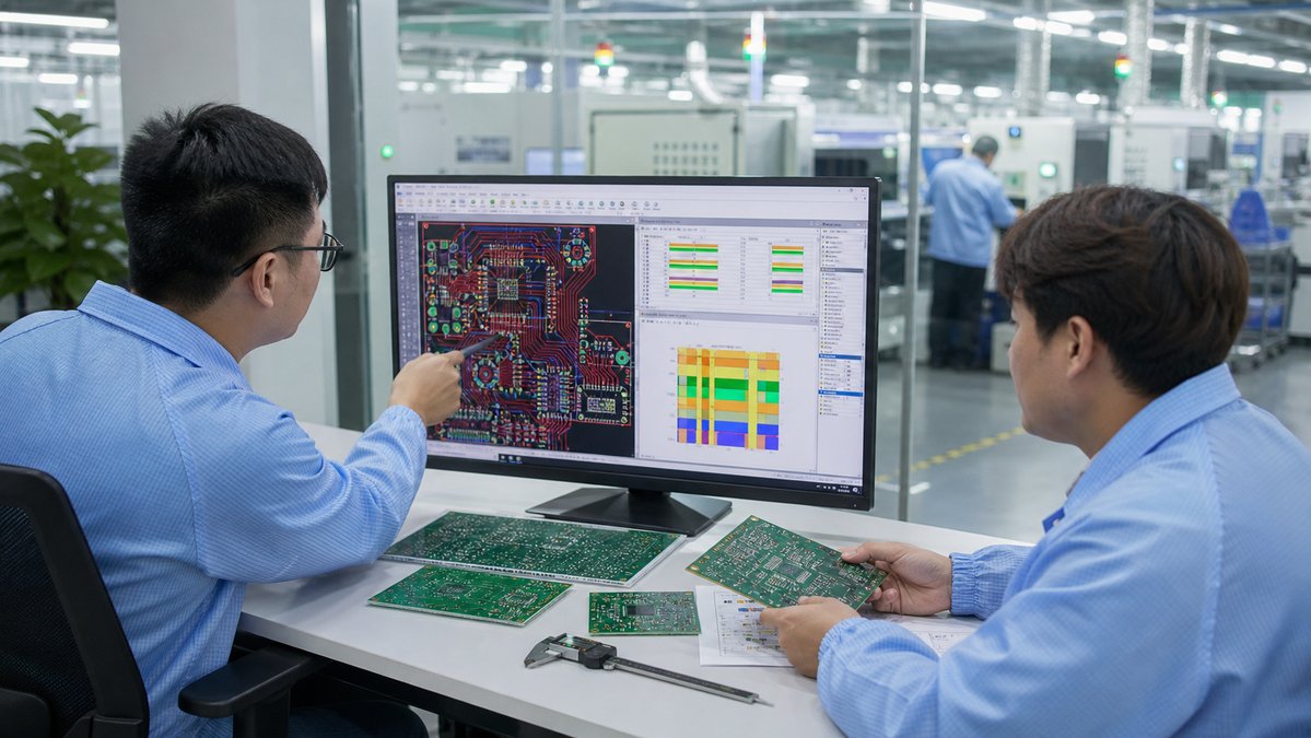
Material selection affects thermal behavior, signal performance, dimensional stability, assembly reliability, and cost. We help customers match material choices to the electrical, mechanical, thermal, and supply-chain needs of the project.
- Low-Tg, mid-Tg and high-Tg FR-4.
- Halogen-free FR-4 and selected high-temperature material options.
- Rogers 4003, Rogers 4350, Rogers 5880 and other RF laminate families.
- Taconic, PTFE, Isola 370HR, Isola FR408HR and Nelco options.
- Aluminum, copper and stainless-steel substrates for metal-core PCB.
- Al2O3, AlN, ZrO2, Si3N4 and other ceramic substrate options by process type.
- Flexible and rigid-flex materials for FPC and compact assemblies.
Material availability should be confirmed with the target thickness, copper type, layer structure, impedance target, quantity, and delivery requirement. For special laminates, we recommend confirming procurement before the layout is frozen.
How Do We Support Turnkey PCBA?
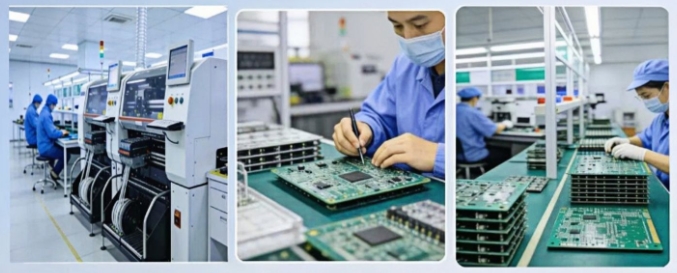
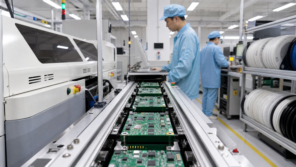
EBest Circuit can continue the project after bare-board fabrication, so customers do not need to coordinate separate PCB, component sourcing, and assembly suppliers for every build.
- SMT assembly.
- THT / DIP assembly.
- Mixed SMT and through-hole assembly.
- Component sourcing.
- Customer-supplied components.
- PCB with wire or cable assembly.
- Box-build assembly.
- Inspection and functional testing.
Customers can choose turnkey PCBA, consigned components, or hybrid sourcing. For turnkey projects, we handle PCB fabrication, component sourcing, assembly, and agreed testing. For consigned or hybrid builds, customers can supply controlled, programmed, allocated, or critical components while we support the remaining manufacturing scope.
What Quality Certifications and Standards Support Our Work?
Quality documentation matters when a PCB or PCBA supplier is part of a formal approval process. EBest Circuit company materials list ISO 9001:2015, ISO 13485:2016, IATF 16949, AS9100D, UL, RoHS, REACH and FPC SGS documentation.
Certification scope can vary by product, process, manufacturing route, and customer requirement. If your project requires a specific IPC class, certificate package, quality document, material record, inspection plan, or customer audit, include it in the RFQ so we can confirm the applicable path before production.
| Certification or Compliance Item | Typical Relevance |
| ISO 9001:2015 | General quality management |
| ISO 13485:2016 | Medical-device-related quality management |
| IATF 16949 | Automotive quality management |
| AS9100D | Aerospace-related quality system requirements |
| UL / UL E502832 | UL recognition and product documentation |
| RoHS / REACH | Environmental compliance support |
| FPC SGS documentation | Supporting documentation for flexible PCB projects |
How Do We Control PCB and PCBA Quality?
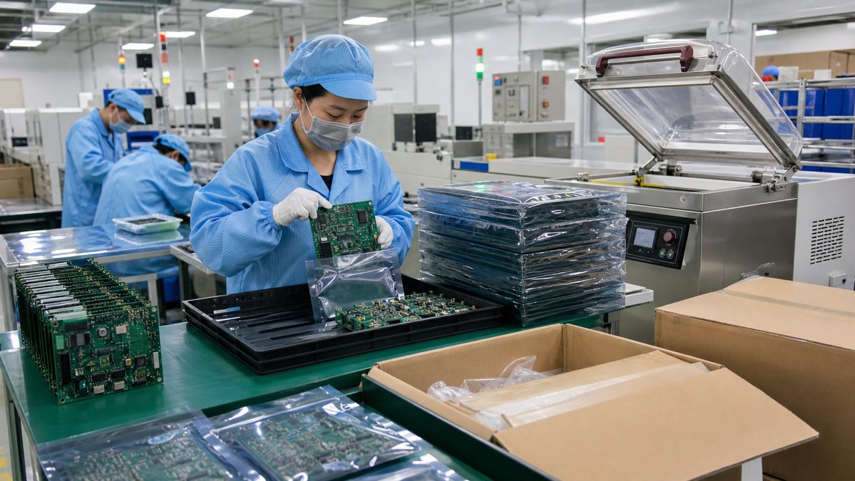
Quality control is built across incoming inspection, fabrication, assembly, final inspection, and shipment. The right inspection plan depends on the board type, component density, end application, and customer requirements.
For PCB fabrication, inspection and measurement may include:
- AOI.
- Electrical testing.
- Flying probe testing.
- Impedance testing.
- Copper-thickness measurement.
- Microsection inspection.
- Hole-diameter measurement.
- Dimensional measurement.
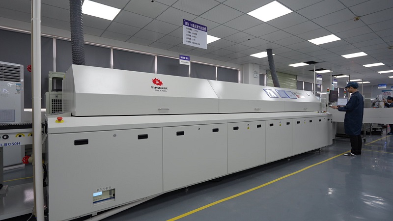
For PCBA production, inspection may include SPI, AOI, X-ray, first-article inspection, functional testing, and project-specific tests. A simple SMT assembly does not need the same test plan as a dense PCBA with BGA, fine-pitch ICs, programmed devices, firmware loading, or critical functional requirements.

What Testing and Inspection Methods Are Available?
Each test method is selected to control a specific manufacturing risk. Customers should specify required testing, fixtures, firmware, procedures, expected outputs, and pass/fail criteria where applicable.
| Inspection / Test | Main Purpose |
| AOI | Checks visible PCB or assembly defects |
| Flying Probe / E-Test | Detects opens and shorts |
| SPI | Checks solder-paste deposition |
| X-Ray | Inspects hidden solder joints such as BGA connections |
| Impedance Test | Verifies controlled-impedance structures |
| Microsection | Examines plated holes and internal construction |
| Copper Thickness Test | Confirms copper thickness |
| Dimensional Measurement | Checks mechanical dimensions |
| FAI / First Article | Verifies the initial build before continuing |
| Functional Test | Confirms agreed electrical or functional behavior |
| XJTAG | Supports applicable boundary-scan or test requirements |
Not every project needs every inspection method. The most efficient test plan is the one that matches the real product risk.
What Lead Time Should You Expect?
Lead time depends on layer count, material availability, copper thickness, board complexity, component sourcing, inspection requirements, testing scope, and production quantity. Prototype and volume production schedules should be reviewed separately.
Reference FR-4 prototype lead times in company materials include:
- Single-layer PCB: 3-4 days.
- 2-layer PCB: 4-6 days.
- 4-6 layer PCB: 6-10 days.
- 8-layer PCB: 10-14 days.
- 10-layer PCB: 14-18 days.
- 1+N+1 / 2+N+2 HDI: about 2.5-3.5 weeks.
For PCBA projects with customer-supplied components, reference prototype assembly lead times include about 1 week for components >=0402 without DIP, about 1-2 weeks for components >=0402 with DIP, about 1-2 weeks for components <=0201 without DIP, and about 1.5-2 weeks for components <=0201 with DIP. BOM purchasing can add time, especially when components are unavailable, allocated, obsolete, or long-lead.
What Should You Send for Engineering Review?
The fastest way to evaluate a PCB or PCBA project is to send the actual files and requirements. Partial files are useful at the early design stage, but a complete package gives a more reliable quotation and manufacturing plan.
For bare PCB review, send:
- Gerber or ODB++ files.
- NC drill files and drill table.
- Stack-up and finished board thickness.
- Material, copper weight and surface finish.
- Impedance, via and tolerance requirements.
- Quantity and target delivery date.
- Required IPC class, certificates or inspection records.
For PCBA review, also send:
- BOM.
- Pick-and-place file.
- Assembly drawing.
- Component sourcing preference.
- Programming requirements.
- Functional-test requirements.
- Expected prototype and production quantity.
If the design is still under development, send the files you already have. We can identify which specifications need to be confirmed before production.
FAQ About Working With EBest Circuit
Can EBest Circuit support both PCB fabrication and PCBA assembly?
Yes. We support PCB fabrication, component sourcing, SMT assembly, THT/DIP assembly, mixed assembly, inspection, functional testing, and selected box-build requirements.
Can you review files before quotation?
Yes. Send Gerber files, drill files, stack-up, BOM, pick-and-place data, drawings, quantities, and test requirements. We can review manufacturability before quotation.
Can customers supply their own components?
Yes. Customers may choose turnkey PCBA, consigned components, or hybrid sourcing. Hybrid sourcing is useful when customers want to control critical ICs or programmed devices.
Can you support prototype builds before production?
Yes. We support prototypes, small-volume builds, and volume production. A project can move through prototype review, design updates, pilot production, and larger production batches.
Can customers arrange a factory audit?
Yes. Customers can arrange an audit as part of supplier qualification. Share the audit checklist, scope, preferred manufacturing site, and proposed date in advance.
What if a PCB is outside the standard process window?
Send the files for engineering review. Special-process items such as 3/3 mil features, 0.15 mm finished holes, high copper weight, more than 10 FR-4 layers, unusual thicknesses, or 10:1 aspect ratio need to be reviewed with the complete stack-up.
Start Your PCB or PCBA Project With EBest Circuit
If you are evaluating EBest Circuit as your PCB and PCBA manufacturing partner, send us the project data you already have. We can review the files, confirm the manufacturing path, raise technical questions, and prepare a quotation based on the actual build.
For bare PCB projects, send Gerber or ODB++ files, stack-up, material, copper weight, quantity, surface finish, and any inspection requirements. For PCBA projects, add the BOM, pick-and-place file, assembly drawing, sourcing preference, programming needs, and functional-test requirements.
Send your PCB or PCBA files to sales@bestpcbs.com for engineering review and quotation.