The TQFP package remains widely used for microcontrollers, mixed-signal ICs, communication devices, motor-control ICs, and other components that need moderate to high I/O counts without moving to BGA packaging. Their exposed gull-wing leads also make them attractive when visual solder inspection, prototyping, and rework matter.
The main challenge is that “TQFP64” or “TQFP100” does not uniquely define a package. Two ICs can have the same TQFP pin count but different body sizes, lead pitches, or overall dimensions. For PCB designers, the correct workflow is therefore part number → package drawing → land pattern, not pin count → generic footprint.
Key Takeaways
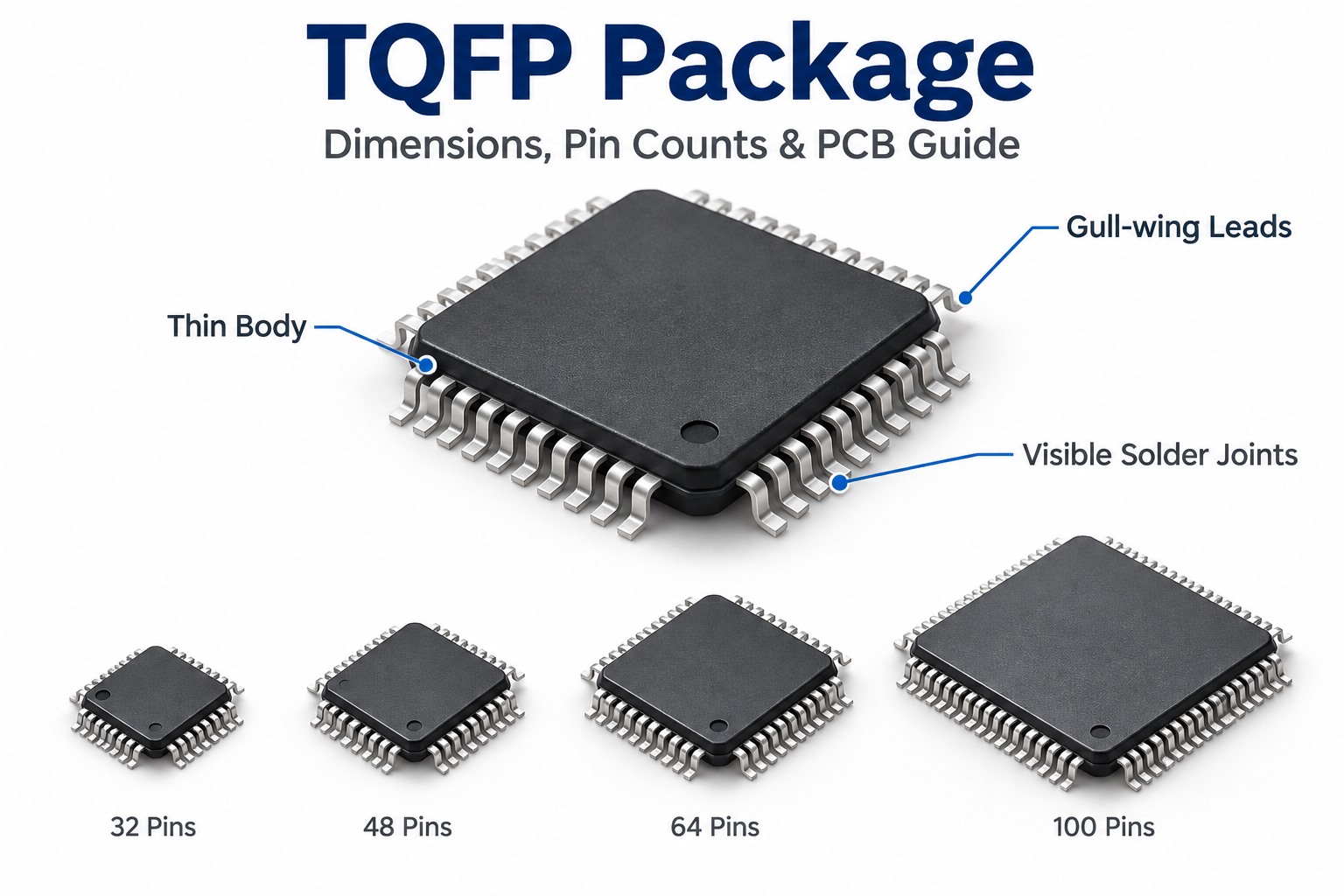
- TQFP stands for Thin Quad Flat Package, a surface-mount IC package with gull-wing leads extending from all four sides.
- TQFP is a package family, not one fixed footprint. Pin count alone does not determine body size, lead pitch, or PCB land pattern.
- Common examples include TQFP32, TQFP44, TQFP48, TQFP64, TQFP100, and TQFP144, but dimensions can vary between semiconductor manufacturers.
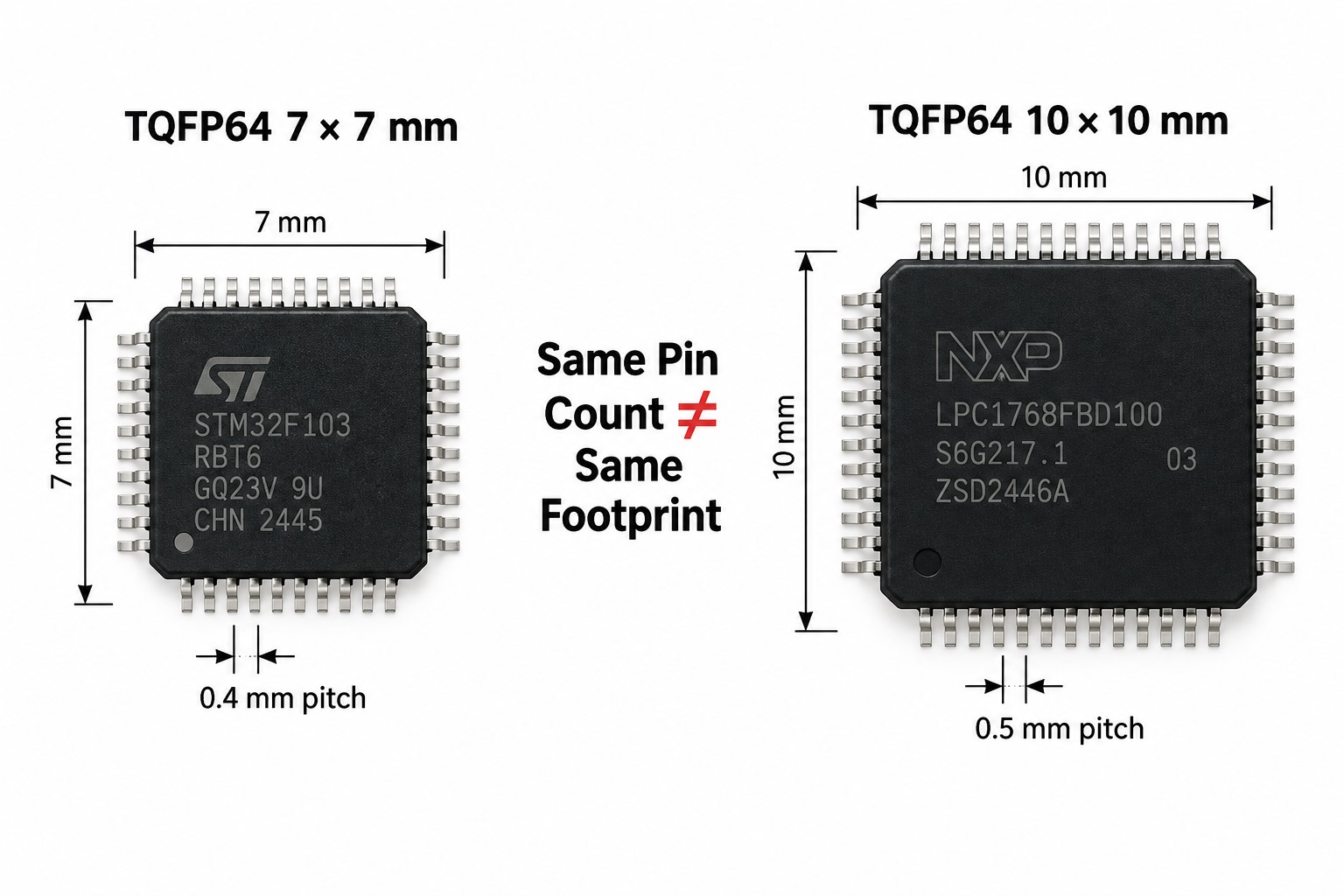
- For example, NXP lists both 10 × 10 mm and 7 × 7 mm TQFP64 packages, showing why “TQFP64” is not enough information for footprint selection.
- TQFP and LQFP are closely related QFP variants, but package names alone do not guarantee footprint compatibility.
- Compared with QFN, TQFP uses visible gull-wing leads, which makes solder-joint inspection and rework easier but requires more PCB area.
- PCB footprints should always be built from the exact manufacturer package drawing, including pitch, body size, overall lead span, lead width, lead length, and package orientation.
What Is a TQFP Package?
TQFP stands for Thin Quad Flat Package, it is a surface-mount package with leads extending from all four sides of a thin molded body. It belongs to the broader QFP, or Quad Flat Package, family. The leads are formed into a gull-wing shape so they can sit on PCB pads and be soldered by standard SMT reflow processes.
Typical TQFP characteristics include:
- Leads on four sides
- Gull-wing lead shape
- Surface-mount assembly
- Relatively low package profile
- Fine lead pitch
- Visible solder joints
- Pin counts from a few dozen to well above 100
A TQFP package is commonly used when the IC needs more I/O than SOIC or similar two-sided packages can provide but the design does not require BGA-level interconnect density.
How Is a TQFP Package Constructed?
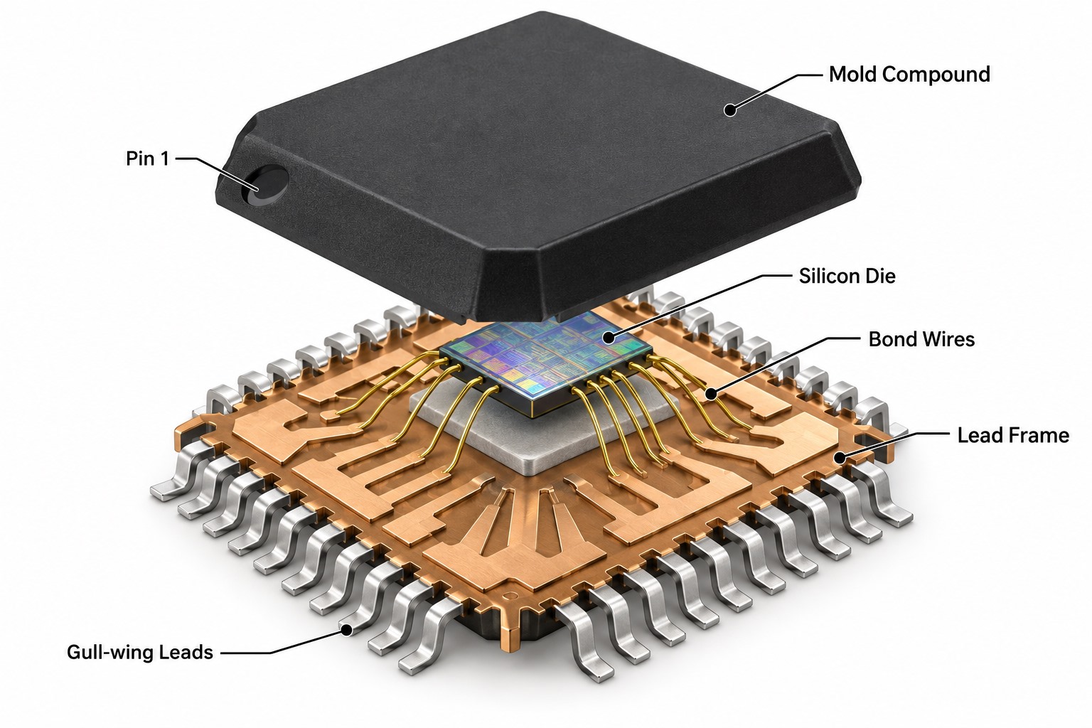
A TQFP package normally contains a silicon die mounted inside a molded plastic body and electrically connected to an external lead frame.
Its basic construction includes:
- Silicon die
- Die attach material
- Bond wires or equivalent internal interconnection
- Copper-alloy lead frame
- Mold compound
- Gull-wing leads
- Pin 1 orientation mark
The lead frame carries signals from the silicon die to the external terminals. After molding, the leads extend outward from all four sides and bend downward toward the PCB.
The package body itself is smaller than the total installed footprint because the leads extend beyond the molded body. This distinction matters during placement and land-pattern design.
What Dimensions Define a TQFP Package?
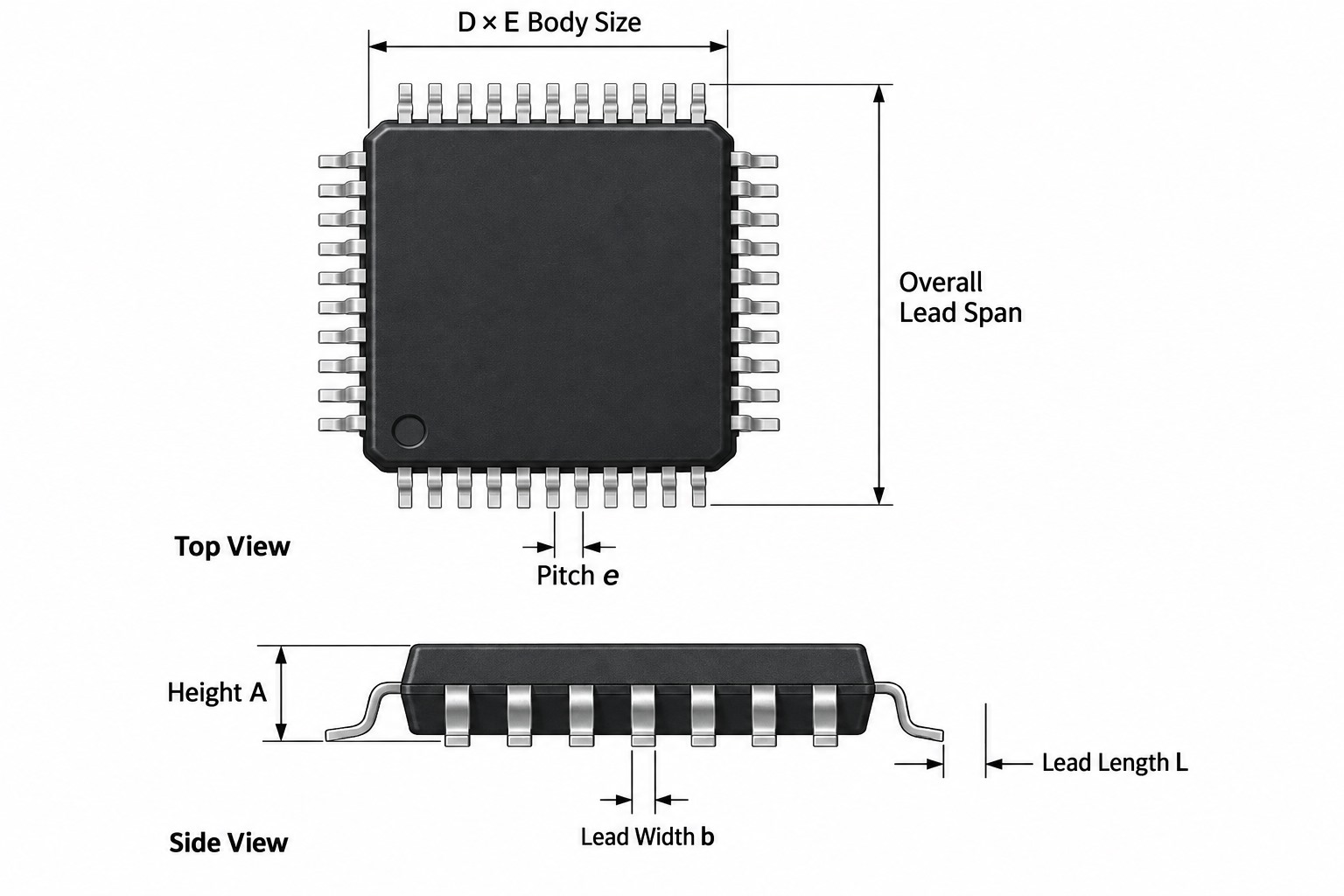
TQFP package dimensions include several mechanical values, not just the molded body width.
| Parameter | What It Describes |
|---|---|
| D × E | Molded body length and width |
| HD × HE or overall D × E | Total span including leads |
| A | Overall package height |
| A1 | Standoff above the PCB seating plane |
| e | Lead pitch |
| b | Lead width |
| L | Gull-wing lead length |
| N | Total lead count |
Body size and overall lead span are not the same dimension. A PCB footprint designed only from the stated body size can miss the additional space occupied by the gull-wing leads.
TQFP32, 44, 48, 64, 100 and 144: What Are the Common Dimensions?
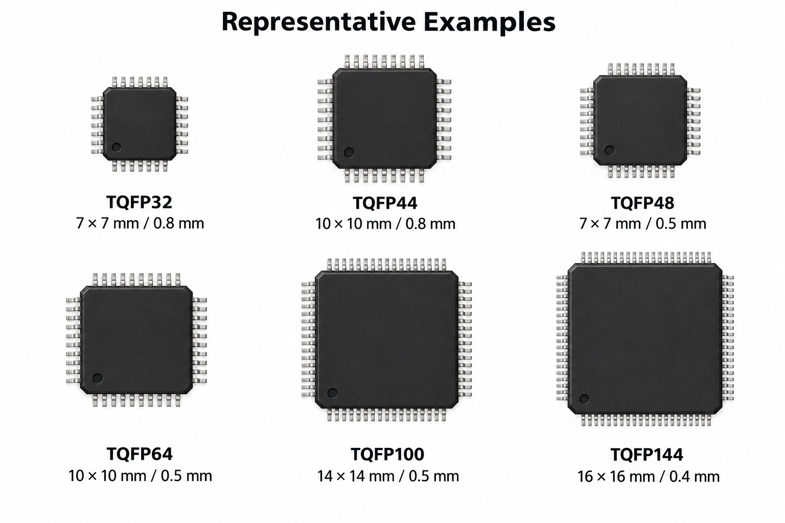
TQFP packages appear in many pin counts, but the following values should be treated as representative package examples rather than universal dimensions.
| Package Example | Representative Body Size | Representative Pitch |
|---|---|---|
| TQFP32 | 7 × 7 mm | 0.80 mm |
| TQFP44 | 10 × 10 mm | 0.80 mm |
| TQFP48 | 7 × 7 mm | 0.50 mm |
| TQFP64 | 7 × 7 or 10 × 10 mm examples | 0.40 or 0.50 mm examples |
| TQFP100 | 14 × 14 mm | 0.50 mm |
| TQFP144 | 16 × 16 mm example | 0.40 mm |
The package name should therefore never replace the exact IC mechanical drawing.
Does the Same TQFP Pin Count Always Mean the Same Footprint?
No. The same TQFP pin count does not guarantee the same body size, lead pitch, lead span, or PCB footprint.
TQFP64 is a clear example. Different vendors offer 64-pin packages in multiple body sizes and pitches, so a CAD library entry named only “TQFP64” is not sufficiently specific for production.
Before reusing a footprint, compare:
- Body dimensions
- Overall lead span
- Lead pitch
- Lead width
- Lead length
- Package height
- Pin 1 orientation
A footprint can look plausible on screen and still be completely incompatible with the physical component.
TQFP vs QFP: What Is the Difference?
QFP is the broader Quad Flat Package family, while TQFP is a thinner-profile member of that family.
Both use:
- Leads on four sides
- Gull-wing terminals
- Surface-mount assembly
- Similar general soldering methods
The difference is mainly in the mechanical outline and package profile. TQFP should therefore not be treated as a package technology completely separate from QFP; it is better understood as a thinner mechanical implementation within the same four-sided leaded package concept.
TQFP vs LQFP: What Is the Difference?
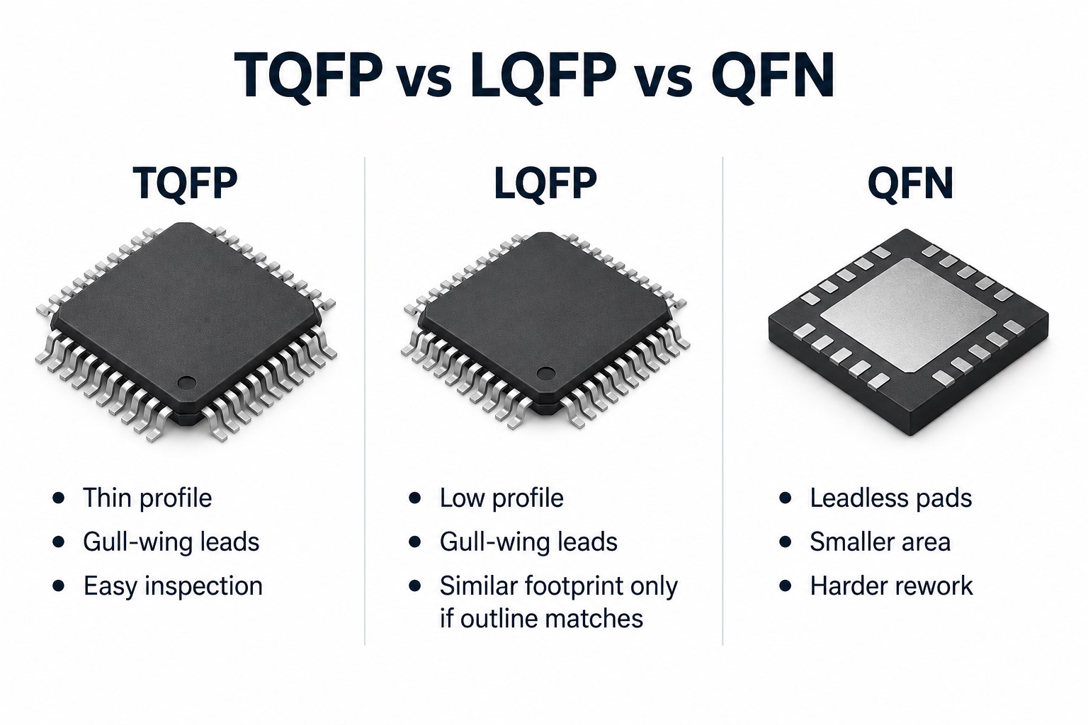
In a TQFP vs LQFP package comparison, both are closely related low-profile QFP variants. Their naming conventions can overlap enough that engineers should compare actual mechanical drawings instead of relying on the acronym.
| Feature | TQFP | LQFP |
|---|---|---|
| Full name | Thin Quad Flat Package | Low-Profile Quad Flat Package |
| Leads | Gull-wing | Gull-wing |
| Mounting | SMT | SMT |
| Typical profile | Thin | Low profile |
| Common pitch range | 0.4–0.8 mm | 0.4–0.8 mm |
| Footprint compatibility | Only if full outline matches | Same rule |
Never assume that TQFP and LQFP are footprint-compatible just because the pin count is the same.
TQFP vs QFN: Which Is Easier for PCB Assembly?
In a TQFP vs QFN package comparison, TQFP is generally easier to inspect and rework because its gull-wing leads and solder joints are visible around the package perimeter.
| Assembly Factor | TQFP | QFN |
|---|---|---|
| External leads | Gull-wing | Leadless bottom pads |
| Solder-joint visibility | High | Limited |
| AOI access | Good | Bottom joints less visible |
| X-ray requirement | Usually not essential | Often useful |
| Manual rework | Easier | More difficult |
| PCB area | Larger | Smaller |
| Fine-pitch defect risk | Bridging / opens | Insufficient wetting / voids |
| Thermal pad | Package dependent | Common on many QFNs |
QFN can save significant PCB area and often offers a shorter electrical and thermal path, while TQFP remains attractive when inspection access and rework matter.
How Should a TQFP PCB Footprint Be Designed?
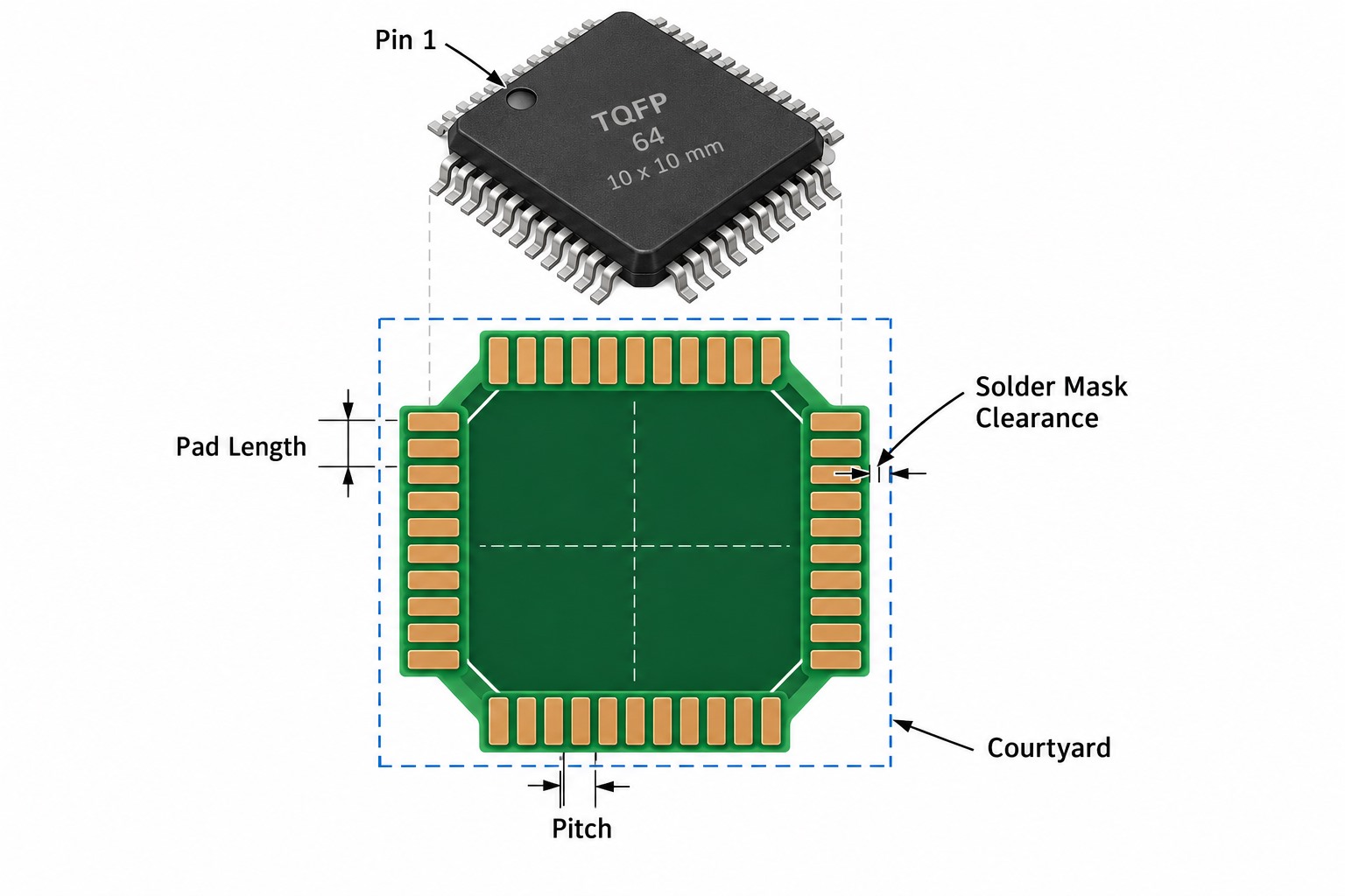
A TQFP PCB footprint should be created from the exact semiconductor manufacturer’s land-pattern or package drawing, not from a generic pin-count template.
Check these dimensions first:
- Lead pitch
- Lead width
- Lead length
- Molded body size
- Overall lead span
- Pin 1 orientation
- Seating-plane information
- Package tolerances
The PCB land pattern must also provide suitable solder fillets around the gull-wing leads. Toe, heel, and side fillets depend on the package geometry and the chosen land-pattern standard.
Also include clear pin 1 marking, solder-mask clearance, silkscreen that does not overlap pads, component courtyard, pick-and-place origin, and adequate neighboring-component clearance.
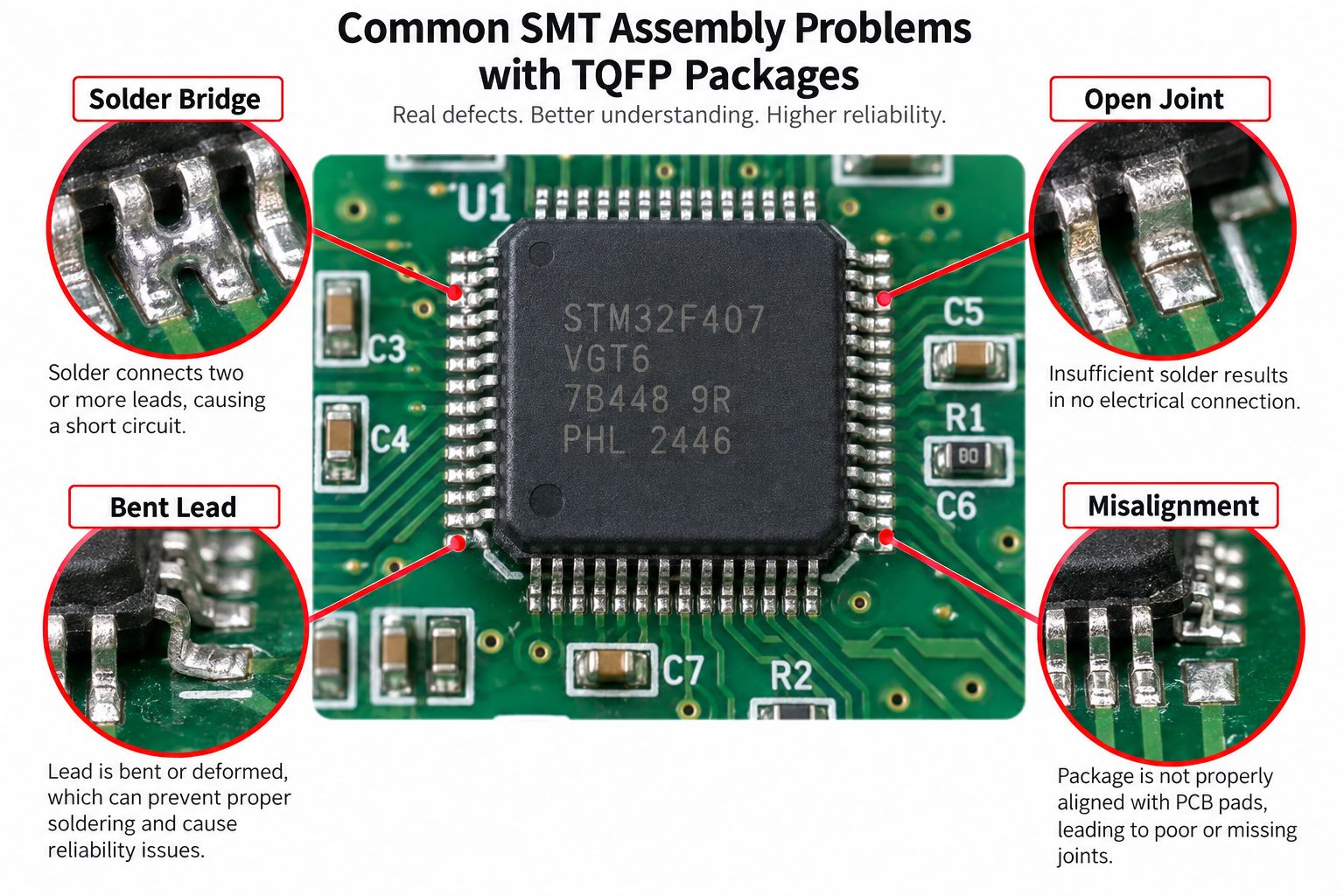
What SMT Assembly Problems Are Common with TQFP Packages?
The most common TQFP assembly defects involve fine-pitch leads, solder-paste volume, placement accuracy, and lead coplanarity.
Typical issues include:
- Solder bridging
- Insufficient solder
- Open joints
- Bent leads
- Lifted leads
- Lead coplanarity problems
- Component misalignment
- Wrong orientation
- Contamination around fine-pitch pads
Solder bridging is especially common when pad geometry, stencil aperture, paste volume, or placement is poorly controlled. Fine-pitch packages leave little margin between adjacent solder deposits.
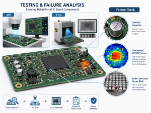
A robust SMT process may use solder paste inspection, accurate placement, controlled reflow, AOI, microscope inspection, and X-ray when hidden structures also require it.
When Is TQFP a Good Package Choice?
TQFP is a practical choice when the design needs a moderate or high pin count while keeping solder joints visible and accessible.
It works particularly well for:
- Microcontrollers
- Industrial control ICs
- Motor-control devices
- Mixed-signal ICs
- Communication controllers
- Prototype and low-to-medium-volume assemblies
- Products where rework access matters
TQFP may be less attractive when the design requires extremely high I/O density, minimum PCB area, very short high-speed interconnects, exceptional thermal dissipation, or package sizes smaller than exposed-lead QFP can provide.
For many industrial, automotive-control, instrumentation, and embedded applications, the additional board area is acceptable because the visible leads simplify inspection and troubleshooting.
FAQ About TQFP Packages
1. What does TQFP stand for?
TQFP stands for Thin Quad Flat Package. It is a surface-mount IC package with gull-wing leads on all four sides.
2. Is TQFP a surface-mount package?
Yes. TQFP is designed for surface-mount PCB assembly and is commonly soldered using SMT reflow.
3. What is the typical TQFP64 package size?
A common TQFP64 example is 10 × 10 mm with 0.5 mm pitch, but 7 × 7 mm TQFP64 packages also exist. Always check the exact IC datasheet.
4. What is the typical TQFP100 package size?
A common TQFP100 example is 14 × 14 mm with 0.5 mm lead pitch. Always verify the actual manufacturer drawing.
5. Is TQFP the same as LQFP?
No. They are closely related QFP variants, but the package profile and mechanical outline can differ. Some specific TQFP and LQFP parts may share a footprint only when all relevant dimensions match.
6. Can every TQFP with the same number of pins use the same PCB footprint?
No. Pin count alone does not define body size, pitch, lead span, or land pattern. A TQFP64, for example, can exist in multiple mechanical outlines.
If you are moving a TQFP-based design into fabrication or assembly, EBest Circuit can review the component package drawing, footprint, pad geometry, stencil requirements, orientation, BOM, and PCBA manufacturability before production. Send your Gerber files, BOM, placement files, and component datasheets to sales@bestpcbs.com for DFM review.