A PCB can have correct electrical routing and still run too hot. The problem is often not the component alone, but the lack of a low-resistance path from its exposed pad into the board.
Designers use thermal vias to provide that path. They move heat through the PCB to internal copper, bottom-side copper, or an external heat sink. They are commonly used under QFN packages, MOSFETs, power ICs, LEDs, processors, and motor-control devices.
Their performance depends on the complete heat path, not just the number of holes. Finished hole size, plating thickness, PCB thickness, via pitch, copper area, filling method, and assembly process all matter.
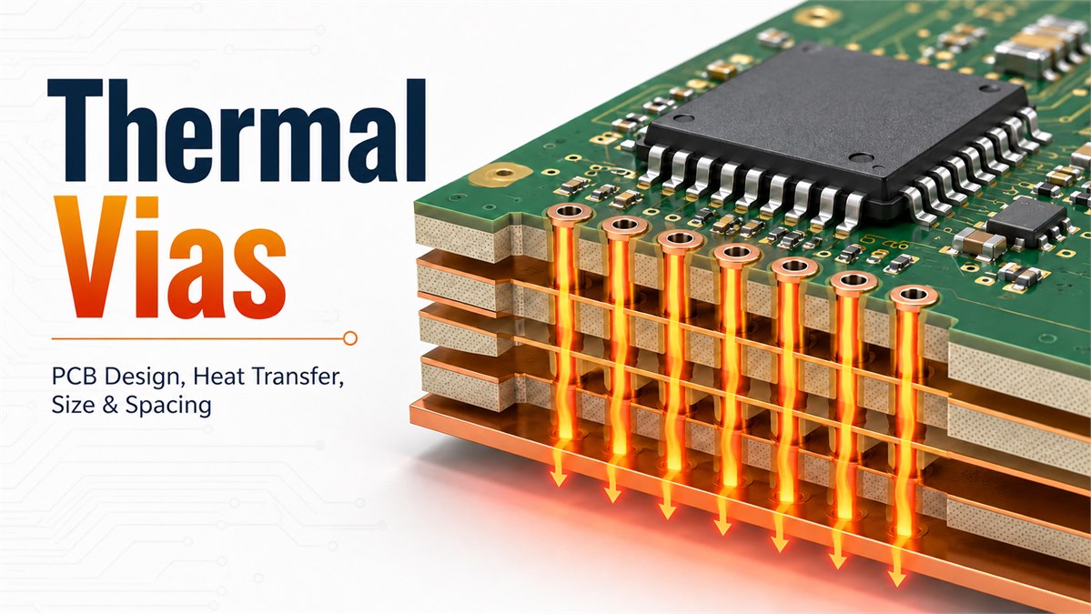
What Are Thermal Vias in PCB Design?
Thermal vias are plated holes used mainly to transfer heat between PCB layers. They normally connect a hot surface pad to internal planes or a bottom-side copper area.
A thermal via may look identical to an electrical via, but its design intent is different. Signal vias are placed where routing requires them. Thermal vias are usually grouped beneath or close to a heat-generating component.
Typical applications include:
- QFN and DFN exposed pads
- Power MOSFETs
- DC-DC converters
- High-power LEDs
- Motor drivers
- RF power devices
- Processors and communication modules
The copper barrel provides the main vertical heat path. FR4 conducts heat poorly compared with copper, so the plated hole wall makes the structure effective.
Thermal vias do not remove heat on their own. They move it to a larger copper area, internal plane, chassis, thermal interface pad, or heat sink. If the receiving copper is too small, adding more vias provides limited benefit.
How Do Thermal Vias Work?
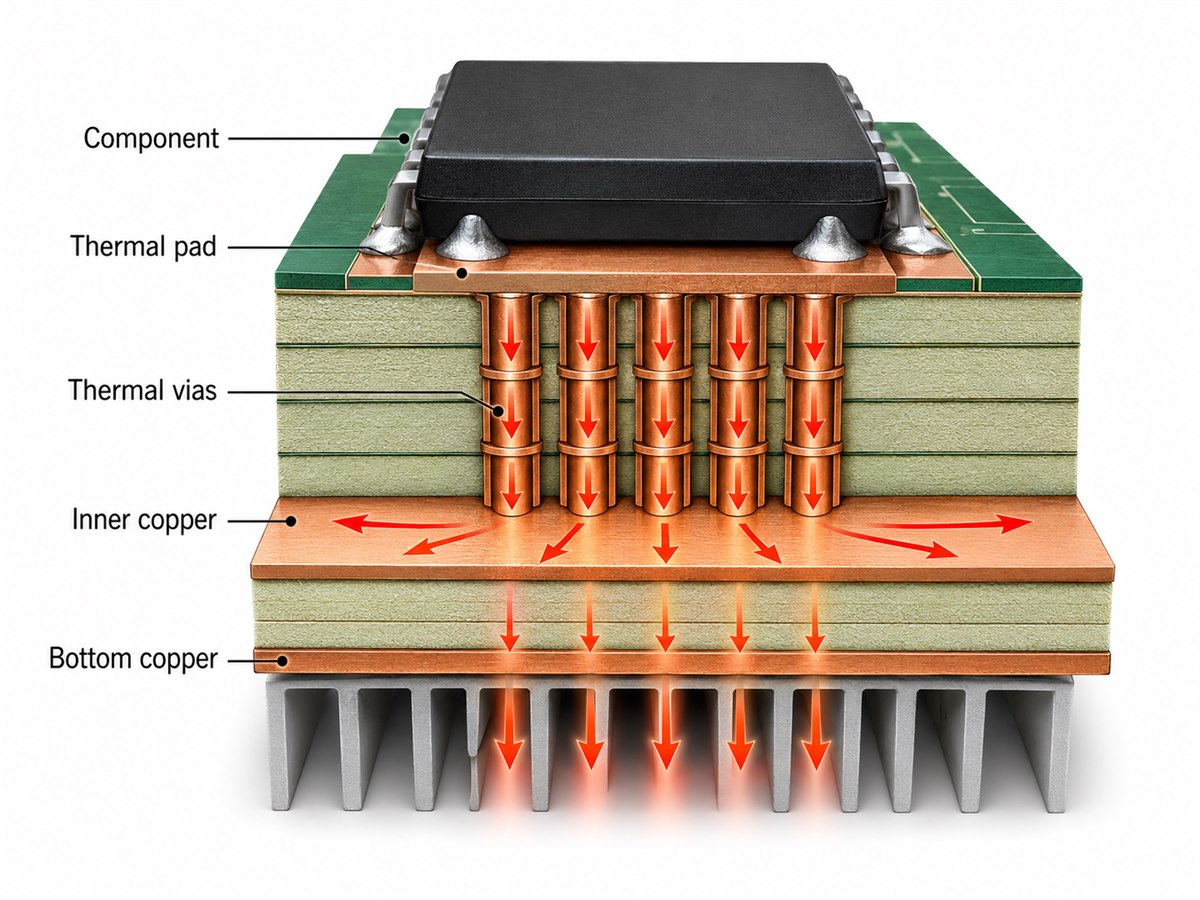
A typical heat path is:
Silicon junction → package pad → solder joint → top copper → via barrels → internal or bottom copper → ambient air or heat sink
The via array performs two jobs:
- Vertical conduction: Moves heat through the board
- Lateral spreading: Feeds heat into larger copper areas
Both are necessary. A dense array connected to a small copper island can perform worse than a moderate array connected to a broad plane.
Board thickness also matters. A longer via has higher thermal resistance. A 3.2 mm PCB therefore needs more careful review than a 1.0 mm or 1.6 mm board using the same hole size.
The final cooling path must also be practical. In a sealed enclosure, bottom copper alone may not dissipate enough heat. Connecting it to a metal housing through a thermal interface material can provide a much larger improvement.
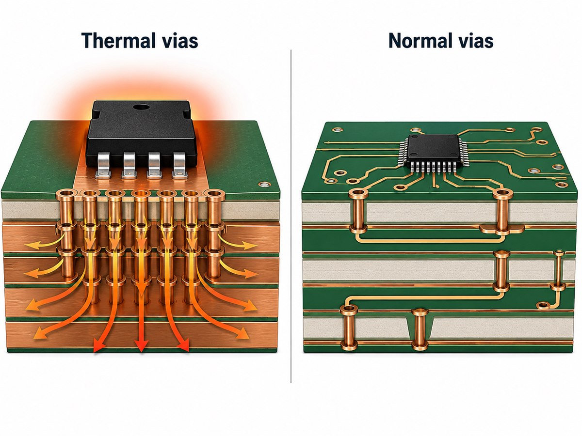
Thermal Vias vs Normal Vias
The main difference is purpose, placement, and connection strategy.
| Design factor | Thermal via | Normal signal via |
|---|---|---|
| Primary function | Heat transfer | Electrical interconnection |
| Typical placement | Under or near hot components | Along signal routes |
| Arrangement | Usually an array | Usually individual |
| Main concern | Thermal resistance | Connectivity and signal integrity |
| Plane connection | Broad copper connection | Trace or assigned plane |
| Filling need | Sometimes required | Usually unnecessary |
A thermal via may also carry current when connected to ground, power, or a MOSFET pad. In that case, thermal and electrical requirements must be checked together.
Thermal vias are not thermal reliefs. A thermal relief reduces heat flow into a plane to improve solderability. A thermal via is intended to increase heat transfer through the PCB.
Where Should Thermal Vias Be Placed?
The best location is usually directly under the exposed thermal pad. This shortens the path from the heat source to the via barrel.
When via-in-pad is not practical, place the vias as close to the hot pad as fabrication and routing rules allow.
Use these placement rules:
- Cover the active thermal-pad area rather than only its edges
- Connect the array to continuous copper
- Avoid narrow copper necks between the pad and vias
- Use solid plane connections unless soldering requires otherwise
- Confirm the exposed pad’s electrical net
- Provide enough bottom or internal copper to spread heat
- Keep temperature-sensitive parts away from the main heat path
A rectangular or staggered array usually works better than a single line of vias under a rectangular pad.
What Thermal Via Size Should You Use?
Thermal vias size depends on board thickness, pad area, plating, filling method, and manufacturing capability; there is no universal finished-hole diameter.
For many standard multilayer PCBs, a finished hole of about 0.20 mm to 0.35 mm is a practical starting point. The final value should come from the component land pattern and the PCB fabricator’s process limits.
Check these dimensions together:
- Finished hole diameter
- Drill diameter
- Via pad diameter
- Annular ring
- Barrel copper thickness
- PCB thickness
- Aspect ratio
Larger holes provide more barrel area, but they consume more pad space and can draw more solder if left open. Smaller holes allow a denser array, but they may increase fabrication cost or require filling.
The fabrication drawing should specify the finished hole size. Drill size alone does not define the final plated diameter.
How Should Thermal Vias Be Spaced?
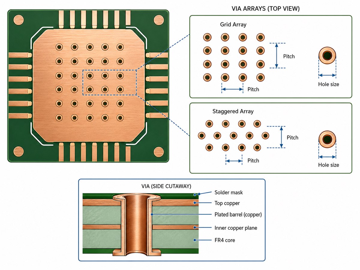
Spacing should balance thermal coverage, copper continuity, drilling capability, and solder behavior.
For many exposed-pad designs, a center-to-center pitch of roughly 0.5 mm to 1.0 mm is a useful starting range. The final pitch must be checked against:
- Finished hole diameter
- Via pad diameter
- Minimum hole-to-hole spacing
- Annular-ring requirements
- Remaining copper between vias
- Stencil and solder-paste design
If vias are too far apart, heat travels farther through the top copper before reaching a hole. If they are too close, the pad becomes heavily perforated and manufacturing becomes more difficult.
Common patterns include rectangular grids, staggered grids, and dense center arrays with wider spacing toward the edges.
How Many Thermal Vias Do You Need?
The quantity should be based on heat load, available area, and the complete cooling path.
A practical process is:
- Estimate maximum continuous and transient power loss.
- Set the maximum acceptable junction or case temperature.
- Review the package manufacturer’s thermal land pattern.
- Estimate one via’s thermal resistance.
- Calculate the ideal parallel resistance of the array.
- Include copper spreading and external cooling.
- Validate the design through simulation or prototype testing.
Nine identical vias have about one-ninth the ideal vertical resistance of one via. The total board temperature does not improve at the same rate because the package, copper plane, interface material, and convection eventually become the main limits.
For a small regulator, a 3 × 3 array may be enough. A high-power MOSFET may need more vias, heavier copper, a chassis connection, or a different substrate.
How Is the Thermal Resistance of a Via Calculated?
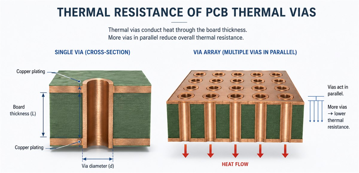
A simplified conduction model is:
Where:
- L is the via length
- k is the thermal conductivity of the barrel material
- A is the effective copper cross-sectional area
For a thin plated barrel:
Where d is the finished hole diameter and t is the barrel copper thickness.
Consider this example:
- PCB thickness: 1.6 mm
- Finished hole: 0.30 mm
- Barrel copper: 25 µm
- Copper conductivity: approximately 385 W/m·K
The simplified thermal resistance is about 176°C/W per via. Nine identical vias provide an ideal array resistance of approximately:
This is not the complete junction-to-ambient thermal resistance. It excludes:
- Package resistance
- Solder-joint resistance
- Copper spreading resistance
- Fill-material effects
- Bottom copper or heat-sink resistance
- Convection and radiation
Use the calculation to compare thermal via designs, not to predict final component temperature by itself.
How Should You Use a Thermal Via Calculator?
A thermal via calculator is useful for screening design options before simulation or testing.
Typical inputs include:
- Board thickness
- Finished hole diameter
- Barrel copper thickness
- Number of vias
- Fill material
- Copper-plane size
- Component power
- Allowed temperature rise
Use finished hole diameter rather than drill-tool diameter. Also enter the specified hole-wall copper thickness instead of relying on a default value.
Compare one change at a time, such as:
- 0.20 mm versus 0.30 mm holes
- Nine versus sixteen vias
- 1.0 mm versus 1.6 mm board thickness
- Open versus filled structures
For automotive, medical, sealed, or high-power products, confirm the result with thermal simulation and prototype measurements.
How Should Thermal Vias Be Designed in a Thermal Pad?
Thermal vias in pad areas provide a short heat path, but they can create assembly problems. Review the related via-in-pad design and fabrication requirements before release.
Open holes may draw solder away from the component pad. Excessive solder wicking can cause:
- Low solder volume
- Voiding
- Package tilt
- Uneven stand-off
- Inconsistent thermal contact
Small open vias may be acceptable in some prototypes, but only when the hole size, stencil aperture, paste volume, and opposite-side termination are controlled.
For fine-pitch or higher-reliability products, filled and capped vias provide a flatter surface. A common process uses non-conductive epoxy filling, planarization, and copper capping.
Review these items together:
- Via diameter and quantity
- Fill and cap requirements
- Surface planarity
- Solder-mask opening
- Segmented stencil apertures
- Allowable voiding
- X-ray inspection criteria
The component manufacturer’s land pattern should be the starting point, then adjusted for the actual PCB and assembly process.
Should Thermal Vias Be Tented, Plugged, Filled, or Left Open?
The treatment depends mainly on whether the via is inside a solderable pad and whether a flat surface is required.
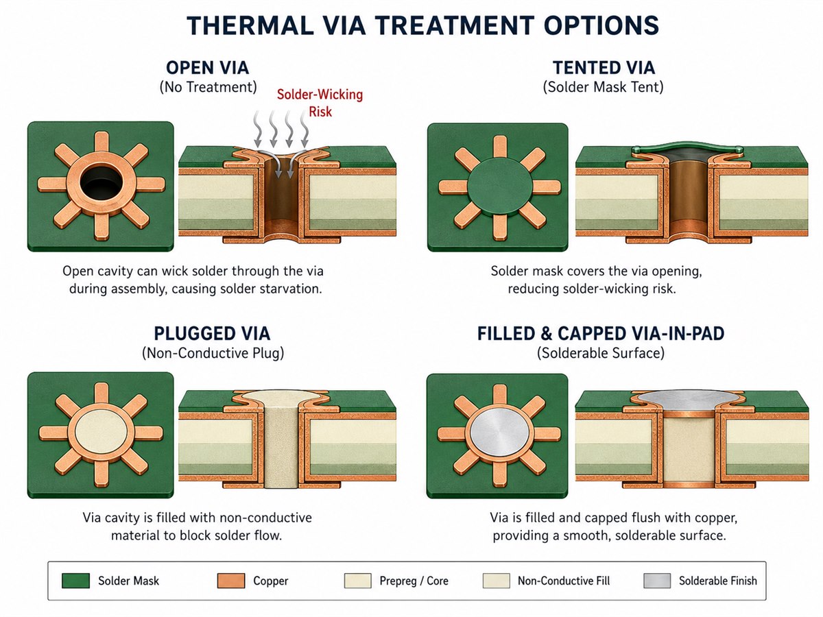
| Via treatment | Best fit | Main benefit | Main limitation |
|---|---|---|---|
| Open | Outside solderable pads | Lowest cost | Can collect solder or contamination |
| Tented | Small vias under solder mask | Protects the opening | Coverage may be incomplete |
| Plugged | Holes that must be blocked | Reduces solder flow | May not create a flat surface |
| Non-conductive filled and capped | Via-in-pad assembly | Flat, stable solder surface | Higher cost |
| Conductive epoxy filled | Selected thermal or electrical use | Adds conductive fill | Lower conductivity than copper |
| Copper filled | Advanced high-performance designs | Strong vertical conduction | Specialized and expensive |
Tenting is not a guaranteed seal. Hole size, mask thickness, and coating side all affect coverage.
Single-sided tenting can also trap moisture or process chemicals. The fabricator may recommend double-sided tenting, plugging, or filling.
For most standard via-in-pad applications, non-conductive fill with copper capping offers a practical balance between assembly reliability and cost.
How Do Thermal Stitching Vias Work with Copper Planes and Heat Sinks?
Thermal stitching vias connect copper areas on several layers so they work as one heat-spreading structure.
A common multilayer arrangement links:
- Top thermal pad
- Internal ground or power plane
- Bottom copper area
- Optional chassis or heat sink
Internal planes spread heat but do not remove much of it from the product. The final temperature still depends on airflow, enclosure design, exposed copper, and any external heat sink.
For chassis-cooled products, review:
- Electrical isolation
- Interface-material thickness
- Surface flatness
- Compression force
- Thermal conductivity
- Mechanical tolerance
If standard FR4 with thermal vias cannot meet the target, alternatives may include IMS, ceramic PCB, copper coins, embedded copper, or direct heat sinking.
What Manufacturing Limits Affect Thermal Via Design?
An effective thermal design must also be repeatable in production.
Check these fabrication limits before release:
- Minimum mechanical drill
- Finished-hole tolerance
- Maximum aspect ratio
- Minimum annular ring
- Minimum via-to-via spacing
- Hole-wall copper thickness
- Fill and planarization capability
- Copper-cap thickness
- Solder-mask tenting limit
- Registration tolerance
- Inspection and microsection requirements
Filled and capped vias require extra process stages, which affect cost, lead time, and yield.
For quotation, provide:
- Gerber and drill files
- PCB thickness and stack-up
- Finished hole and pad dimensions
- Copper weight
- Hole-wall copper requirement
- Fill, plug, or cap notes
- Surface finish
- Solder-mask opening
- Production quantity
- Reliability class and inspection requirements
At EBest Circuit, we can review thermal via arrays, via-in-pad structures, stack-up, fill notes, and assembly conditions before quotation. Clear fabrication notes are important because similar-looking layouts can require very different processes.
What Are Common Thermal Via Design Mistakes?
- Adding many vias without enough receiving copper
- Placing the array too far from the heat source
- Treating the via as a solid copper cylinder
- Ignoring board thickness and hole-wall copper
- Using large open holes beneath solderable pads
- Connecting the exposed pad to the wrong net
- Copying a reference pattern without checking actual power loss
- Assuming conductive epoxy performs like copper
- Ignoring stencil segmentation
- Using one-sided tenting without process review
- Relying on a calculator without prototype testing
FAQs About Thermal Vias
What is the purpose of thermal vias in PCB design?
Their purpose is to conduct heat through the PCB from a hot component pad to internal copper, bottom copper, or an external cooling structure. They reduce the vertical portion of the board’s thermal resistance.
How do thermal vias work?
Copper plated onto the hole wall conducts heat through the board. The connected copper planes then spread the heat over a larger area or transfer it to a heat sink.
What size should thermal vias be?
A finished hole between approximately 0.20 mm and 0.35 mm is a common starting range for conventional thermal-pad arrays. The final size depends on board thickness, aspect ratio, pad area, filling process, and fabrication capability.
How many thermal vias should I use?
The quantity should be based on component power, allowable temperature rise, available pad area, board thickness, via dimensions, and the external cooling path. The component manufacturer’s recommended land pattern is a useful starting point.
Should thermal vias be placed directly under a component?
They should normally be placed directly under an exposed thermal pad when the package, electrical net, fabrication process, and assembly method allow it. This position minimizes lateral heat-travel distance.
Should thermal vias be tented?
Tenting may be suitable for small holes outside solderable pads. Via-in-pad designs usually need more controlled treatments such as plugging or filling and capping.
Should thermal vias be filled with solder?
Intentionally filling ordinary vias with solder is not always reliable because voids can remain and the solder distribution may be inconsistent. A specified resin-fill or copper-fill process provides better process control.
Do filled vias transfer more heat than open vias?
They can, but the improvement depends on the filling material. Conductive epoxy transfers more heat than air but generally much less than copper. Copper-filled structures offer stronger conduction but cost more.
Can thermal vias connect to a ground plane?
Yes, when the component’s thermal pad is electrically connected to ground. Always confirm the package pin definition before connecting the via array to any plane.
Are thermal vias the same as thermal reliefs?
No. Thermal vias increase heat transfer through the PCB. Thermal relief spokes restrict heat flow between a solder pad and a large copper area to make soldering easier.
What is the difference between thermal vias and normal vias?
Their physical construction may be similar, but thermal vias are arranged and connected specifically for heat transfer. Normal vias are mainly used for electrical routing.
Can thermal vias replace a heat sink?
They can reduce PCB thermal resistance, but they cannot always replace a heat sink. High-power devices may still require a chassis connection, metal substrate, heat spreader, airflow, or external heat sink.
Conclusion
Thermal via performance depends on the complete heat path: component pad, via barrels, copper planes, interface materials, and external cooling. More vias are useful only when they connect to enough copper and remain compatible with fabrication and soldering requirements.
For an accurate quotation, provide the Gerber files, stack-up, finished hole dimensions, copper specifications, via-fill notes, assembly requirements, and expected production quantity.
For thermal via DFM review, via-in-pad fabrication, multilayer PCB production, or PCBA assembly, contact EBest Circuit at sales@bestpcbs.com.