If a point-to-point SPI clock rings, check the signal at the receiving pin before changing the resistor. A second crossing of the receiver’s switching region is more important than how tidy the waveform looks at the driver. First rule out probe-induced ringing. Then compare the original board with a source resistor estimated from trace impedance minus effective driver impedance.
This guide follows one hypothetical 3.3 V clock from a controller to a single high-impedance peripheral. It explains what to measure, which resistor to try, and when the result is good enough to release. The numbers are examples, not measured performance or universal limits.
Source Series Termination
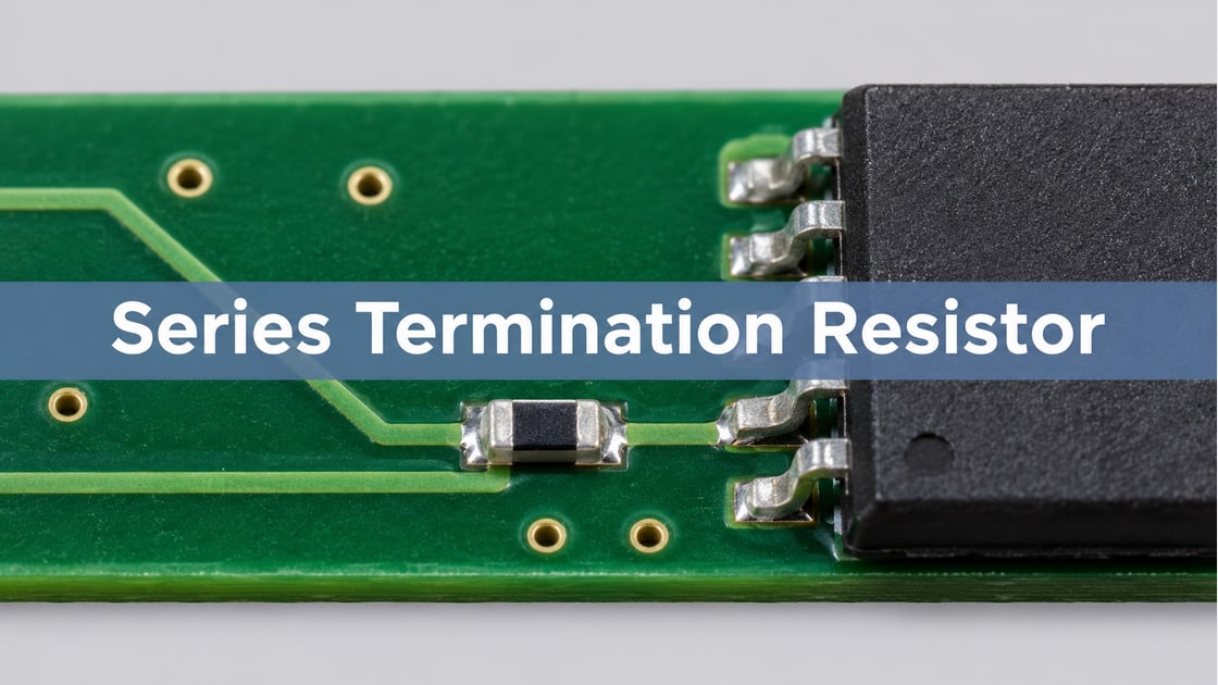
Source series termination puts a resistor between the output pin and the transmission line. The resistor and driver impedance together approximate the trace impedance. The first step travels to the receiver. At a nearly open load, the returning wave is absorbed at the matched source instead of repeatedly reflecting.
On an ideal 3.3 V rising edge with 50 Ω total source resistance and a 50 Ω line, the launched step is 1.65 V. The ideal open load doubles that incident step to 3.3 V. A real receiver has input capacitance and package parasitics, so the waveform will not exactly follow that example. A two-step waveform at the driver side of the line is not, by itself, proof that the receiver missed an edge.
Clock Signal Ringing
Measure at the receiving pin or the closest accessible pad. Use a short probe return and enough bandwidth to see the edge; keep the probe and acquisition settings fixed for each comparison. If apparent ringing changes substantially when you shorten the return, resolve the measurement artifact before tuning the board. Keep the capture time base wide enough to see settling and tight enough to distinguish closely spaced crossings.
Inspect rising and falling edges, not just the largest overshoot. Compare the excursions with the actual receiver’s datasheet voltage limits and input thresholds. If the waveform re-enters the undefined band, do not assume it clocked cleanly. Check transaction errors and, where available, compare the waveforms against receiver timing and hysteresis specifications.
Series Termination Resistor Calculation
Start with Rseries ≈ Z0 − Rdriver. For a nominal 50 Ω trace and a hypothetical effective 18 Ω output impedance, the estimate is 32 Ω; 33 Ω is a practical first build. Do not use the input pin impedance in place of driver impedance. Use an IBIS model or vendor data for a better estimate at the applicable voltage, drive setting and transition. Pull-up and pull-down impedances can differ.
| Input | Illustrative value | What to verify |
| Trace impedance | 50 Ω nominal | Confirm routed geometry and stackup |
| Effective output impedance | 18 Ω assumed | Check IBIS or vendor data for both transitions |
| First resistor trial | 33 Ω | Compare against 0 Ω and adjacent values |
| One-way flight time | 0.67 ns for 100 mm at 150 mm/ns | Use the board’s actual propagation delay |
| Nominal round trip | 1.33 ns | Compare with measured edge and reflection spacing |
Series Termination Resistor Placement
Route from the driver to the resistor first, then from the resistor into the controlled-impedance trace. Keep the driver-to-resistor segment short enough that it does not itself behave like a meaningful unterminated line for the edge in question. Do not leave a branch to an unpopulated alternate footprint or add a long measurement stub. Place any receiver test access where it can be probed without turning it into a branch.
For a board already fabricated, use the intended source resistor footprint if available. A component bodged near the receiver does not test source termination. Record the resistor package and placement along with the tested value so the result can be reproduced.
PCB Trace Impedance
Use the actual edge time, not the clock’s repetition rate, to decide whether reflections matter. A modest-rate SPI clock can still have a fast transition. Obtain the line impedance from the actual fabrication stackup, with the trace referenced to a continuous plane. A split plane, poorly referenced layer transition or branch can produce a separate discontinuity that changing the source resistor cannot repair.
In the example, an apparent interval near 1.33 ns can justify inspecting a 100 mm path, but the estimate does not uniquely identify the reflection source. Check the actual route and compare both ends. If the measurement setup cannot resolve the expected interval, treat that as a limitation, not evidence of a clean edge.
Series Termination vs Parallel Termination
Choose the termination by load placement and drive budget. A clean point-to-point receiver waveform with small power cost often favors a source resistor. If the receiver-side termination needs to suppress the initial load reflection, a suitable parallel network can do so, but its DC or bias loading must be designed for the driver and logic levels.
| Method | Use it when | Reason to change approach |
| Source series | One driver feeds one high-impedance receiver at the end of a line | Intermediate taps see a partial step or edge timing becomes marginal |
| Receiver-end parallel | The far end needs a matched load and the driver can supply its current | DC loading or bias compromises voltage margin or power |
| Topology correction first | A branch, stub or broken return path dominates the waveform | A resistor change does not remove the discontinuity |
SPI Series Termination Resistor
Capture the baseline with 0 Ω, then try 22 Ω, 33 Ω and 47 Ω with the same cable, probe setup, drive strength and stackup. These are example trial values, not a mandated set. Inspect the receiver for excessive overshoot, undershoot, threshold re-entry and slow transitions. Also capture clock and data together, because a slower clock crossing changes setup and hold margins.
Release the smallest set of settings that passes on representative boards and under applicable voltage and temperature corners. Check both edge polarities, worst-case SPI activity, datasheet input limits and functional error rate. Document the test conditions and the chosen resistor. If all values fail, revisit measurement, topology, return path and driver slew before increasing resistance again.
Source Termination vs Load Termination
Probe both the receiver and, separately, the line side of the source resistor. A source match expects a return from the load; a load match is meant to absorb energy at the load. A two-step source waveform with a clean far-end transition can be consistent with source termination. Conversely, a visually clean source waveform does not prove adequate margin at the receiver.
Choose from the receiver’s actual failure mode. Keep source termination if the single end receiver passes voltage, switching and timing checks. Consider load termination only if its bias and current budget are acceptable. If the clock branches to several loads, model or measure each branch instead of carrying over a resistor chosen for a point-to-point design.
Frequently Asked Questions
Does a series resistor go near the clock source or near the receiver?
Place it near the driver for source termination. The resistor and output impedance must appear in series at the launch point of the line. A resistor near the receiver does not provide the same source match. A far-end parallel load is a different termination strategy.
Is 33 Ω always the right SPI clock series resistor?
No. It is a starting value for the example in this guide, where the line is 50 Ω and the output is assumed to be 18 Ω. A different stackup, drive strength, output impedance or receiver loading can make a different value work better.
Why did my clock work only when I touched it with a probe?
A probe can change the effective load, and its return can change the captured waveform. Treat the observation as a clue, not a fix. Repeat with a short return or lower-capacitance probe, inspect the layout and confirm that the circuit passes with the test equipment disconnected.
Can a low SPI clock frequency still cause ringing?
Yes. Reflections depend on the transition edge time and interconnect delay, not only on the clock frequency. Slowing the bit rate can help settle some signals between transitions, but it may not eliminate a receiver threshold re-crossing on a single fast edge.
Why does the source waveform show two steps?
The first step is set by the divider between the source resistance and the line impedance. A high-impedance load reflects the incident wave, which then returns to the source. Inspect the receiving pin to determine whether the receiver sees a single clean edge.
Will the same source resistor work with several SPI slaves?
Not necessarily. The inactive devices and branches can still load the clock line. Intermediate taps can see a partial step or branch reflection. Evaluate each receiving pin with its actual branch lengths and input loads, and consider changing the routing or adding buffering when appropriate.
Can too much series resistance create errors?
Yes. Excess resistance can slow the receiver transition or shift the time at which it crosses the switching region. Check setup and hold with the clock and data captured together. Do not choose a value solely because it gives the smallest overshoot at one test point.
What should I capture before approving the resistor value?
Record the receiver waveform for both polarities, the source-side waveform, the clock-to-data timing, voltage limits and representative transactions. Include drive settings, probe configuration and the board revision. Where the product requires it, repeat across supply and temperature limits before approving the value.
References
- Altera AN 958: Series Termination
- Infineon AP32488: PCB and High-Speed Interface Design Guidelines
- BestPCBs guide to transmission-line termination techniques
Discuss Your PCB Requirements
Preparing a controlled-impedance board for fabrication? Send the proposed stackup, target impedance and trace geometry to Best Technology at sales@bestpcbs.com. Include the layer transitions or connector locations that matter to your design review.