A DDR5 RAM PCB is the circuit board inside a DDR5 memory module. It connects the edge contacts to the DRAM devices, distributes power and carries management signals. The motherboard is a separate PCB: it connects the processor to the memory socket. Both boards affect whether the memory channel works, but their layout rules are not interchangeable.
Imagine a workstation prototype that passes with one module in each memory channel. The next build adds a second module to each channel. Before blaming the new modules for a training failure, check whether the processor, board design and firmware support that population at the intended rate. A DIMM that works by itself does not prove that the fully populated channel has enough margin.
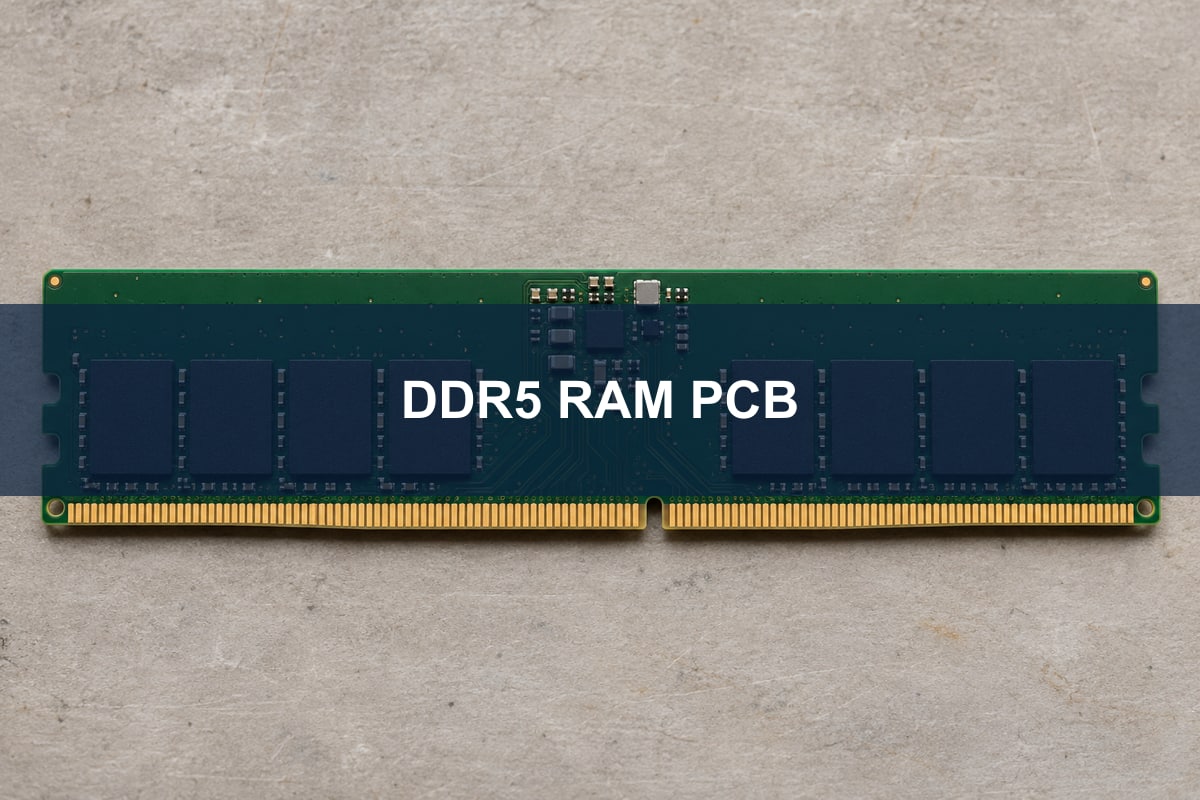
What is on a DDR5 RAM PCB board?
A typical client DDR5 DIMM carries DRAM packages, a power management integrated circuit (PMIC) and a serial presence detect (SPD) hub. The DRAM stores data. The PMIC regulates power locally, and the SPD hub provides configuration information that the platform can use during initialization. Additional devices depend on the module family; do not assume that an unbuffered, registered or clocked DIMM has the same circuit.
A standard non-ECC client DDR5 DIMM divides its data interface into two independent 32-bit subchannels. That split is inside the module interface; it does not mean that plugging in one DIMM populates two motherboard memory channels. When reviewing a diagram, identify whether “channel” refers to the processor’s memory interface or a subchannel within the DIMM before counting sockets or drawing routes.
How to read a DDR5 DIMM pinout
Start with the drawing for the exact module and socket. First verify the contact orientation and mechanical key, then group the contacts by function. Data signals are commonly called DQ; DQS strobes accompany groups of data signals. Clock and command/address signals have separate timing relationships. Power, ground and management contacts must be checked against their own requirements.
On the schematic, verify the connector symbol against the mating drawing, including front and back contact numbering. Next, trace each data group and its strobe back to the controller. A bus that looks connected can still fail if a net swap crosses a group that the controller does not allow. Resolve that discrepancy before using layout tuning to compensate.
DDR5 vs DDR4: What changes on the board?
DDR5 is not a drop-in replacement for DDR4. A desktop module may look similar, but the key position, pin assignment, power design and signaling differ. Compare matching classes of modules rather than treating all DIMMs and SO-DIMMs as interchangeable.
| Decision point | DDR4 client DIMM | DDR5 client DIMM |
| Data interface, non-ECC example | One 64-bit data channel per module | Two independent 32-bit subchannels per module |
| Nominal DRAM operating supply | 1.2 V | 1.1 V; this is not the socket input voltage |
| Module power architecture | Regulation generally on the host board | Local PMIC on the module |
| Mechanical and electrical fit | Use a compatible DDR4 socket and platform | Use a compatible DDR5 socket and platform |
The practical implication for a redesign is that an old connector footprint, rail plan or set of routing constraints cannot be reused as-is. Start with the controller’s DDR5 documentation and the exact module specification, then review the two together.
Inputs for DDR5 RAM PCB design
Freeze the controller, module family, supported slot populations and target data rate before setting routing rules. For example, at a hypothetical design target of 5,600 MT/s, one data unit interval is approximately 179 ps. That number describes the transfer period, not how much skew a route may consume. Get the actual limits from the controller guide for the supported topology.
| Parameter to release | Where to check it | What to record |
| Rate and population | Controller guide and platform support matrix | MT/s, module family, ranks and supported sockets per channel |
| Impedance and spacing | Controller routing table and approved PCB stackup | Single-ended or differential target in Ω, tolerance, layer and reference |
| Timing and skew | Signal-group constraints and package delay data | Limit in ps, allowed swaps and included path segments |
| Power and sideband | Module specification and schematic | Input rails, power sequence and management connectivity |
Compare values from documents only when they describe the same controller, module and segment. The published Altera tables, for example, distinguish signals and routing segments for one DIMM per channel. They illustrate how to read a constraint table, not what values to copy into an unrelated design.
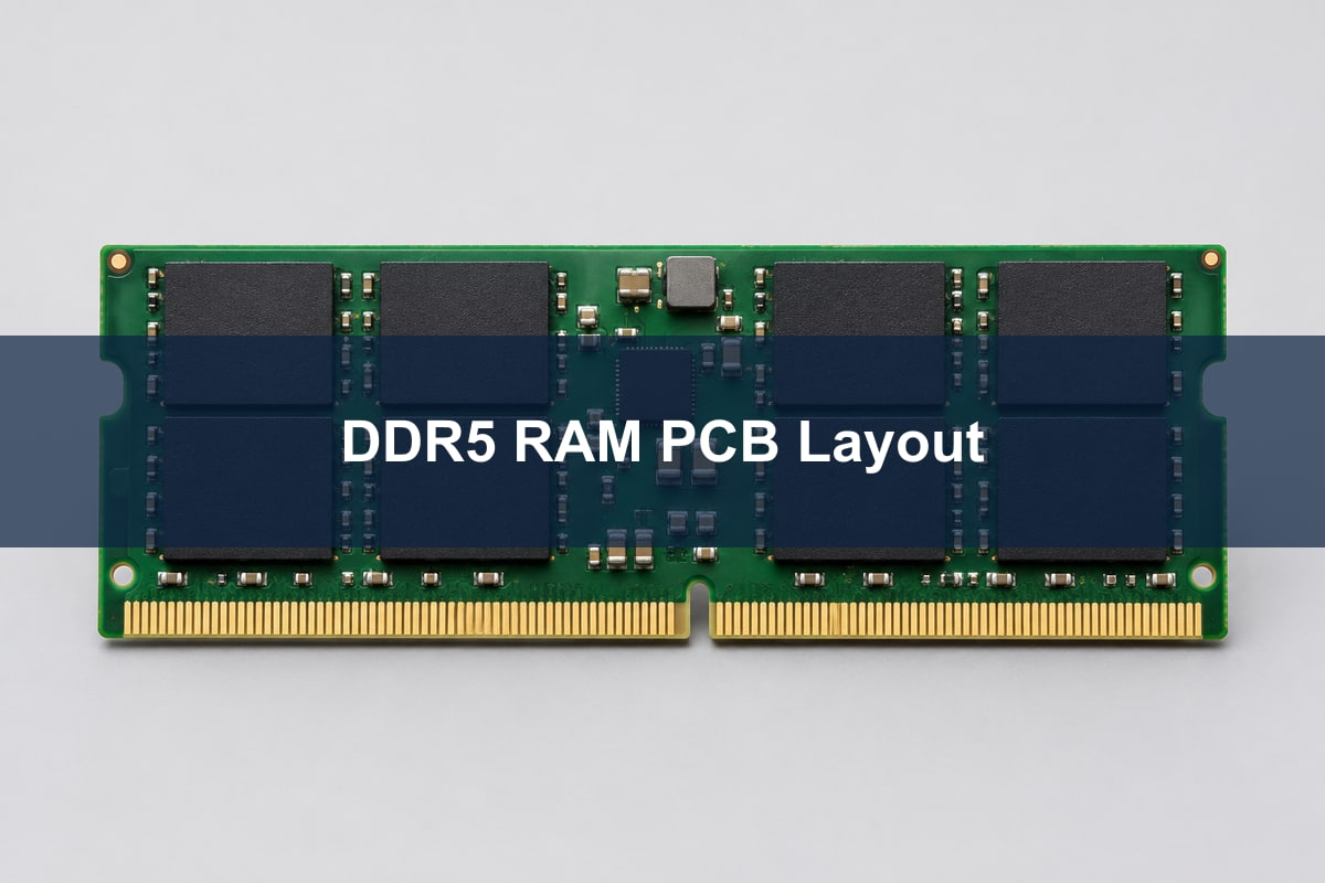
What to check in a DDR5 RAM PCB layout
Check timing against the electrical path, not just the length displayed in the layout editor. Package routing contributes delay, and traces on different layers may propagate at different speeds. Length matching by itself can therefore hide a timing error. Use the controller’s grouping and delay conventions for DQ, DQS, clock and command/address nets.
Open the approved stackup, the CAD timing report and the controller constraint table together. Verify the signal and reference layers, finished dielectric height and any package delay applied to each group. If the group passes in physical length but fails in time, check the layer assignments and package assumptions before adding more tuning. Also inspect the return path at plane transitions; a continuous-looking trace can cross an opening in its reference.
DDR5 routing topology: Follow the signal groups
Different signal groups can follow different paths. A command/address route feeding several devices can have an ordered chain, while a data group and its strobe need to be checked against the devices and connections they actually serve. Do not apply a fly-by rule to every net or use module-side routing guidance for the host escape.
Draw the processor, socket or soldered DRAM and each branch for the group in question. Mark package, PCB and connector segments separately. If the board uses memory down rather than a socketed module, remove the connector assumption and use the controller’s memory-down rules. If a second socket introduces a branch or a different load, use the model for that population rather than stretching the single-socket routing rules.
DDR5 1DPC vs 2DPC: When the design check changes
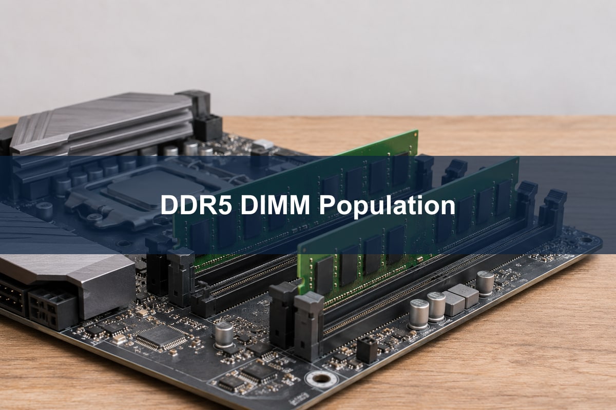
One DIMM per channel (1DPC) and two DIMMs per channel (2DPC) are different configurations. Check both how many sockets the board routes and how many modules are fitted. A two-socket channel with one socket empty is not necessarily electrically identical to a design with only one socket; unused routing can remain part of the channel.
In the workstation example, keep the board, firmware and module family fixed. First test the supported single-module population using the specified socket. Then add the second qualified module and verify the supported speed and rank combination for the new population. If the original target is no longer supported, qualify the supported lower rate or revisit the topology. Do not treat an unsupported high-speed boot as proof of usable margin.
What DDR5 memory training can tell you
Memory training is part of initialization: the controller and firmware calibrate settings for the installed channel. A training failure is a symptom, not a diagnosis. First compare the actual population, firmware version, default data rate and reported failure stage against a known-good configuration.
For a board bring-up, change one variable at a time and record the trained rate, detected capacity and repeated cold-start results. If only the fully populated case fails, review topology, supported speed, power and routing evidence before assuming a bad DIMM. If it trains successfully, still run the agreed memory stress tests under relevant operating conditions. A passing bare-board impedance result supports the represented trace construction, not assembled channel timing. See the high-speed interconnect validation guide for the distinction between physical connectivity and demonstrated link performance.
FAQ
Does DDR5-5600 mean a 5,600 MHz clock?
No. The designation refers to 5,600 million transfers per second per data pin. Do not use that transfer rate as the clock frequency or as a complete timing budget.
Is one DDR5 DIMM the same as dual-channel motherboard memory?
No. The two subchannels within a DIMM and the processor’s motherboard channel population are different levels. Follow the platform slot map.
Does on-die ECC make a standard DIMM a system ECC module?
No. On-die ECC operates inside the DRAM device. End-to-end memory error protection also depends on the module and controller interface and platform support.
Can UDIMM and RDIMM be mixed?
Do not assume compatibility. The registered module has a different command/address architecture. Use the platform’s supported module classes and population rules.
Is there a universal DDR5 PCB layer count?
No. Routing density, escape geometry, reference planes, power delivery and the manufacturing process determine the stackup. A layer count alone does not establish signal integrity.
Should I always use the second socket first?
No. Slot names and recommended population order are board-specific. Use the motherboard or platform manual, not the physical position alone.
What should I record when a memory test passes?
Record the actual rate, firmware, slot population, module part numbers, test duration and relevant operating conditions. The result only supports the configuration that was tested.
What should I send for a PCB fabrication review?
Send the approved stackup, routed signal groups, impedance targets and tolerances, fabrication files and coupon requirements. Separate any request for assembly or system-level validation from the bare-board requirements.
Technical references
- Micron: DDR5 client module features
- Micron: DDR4 and DDR5 device characteristics
- Intel: DDR5 module routing and package skew
- AMD: Platform-specific physical design rules
- Altera: One-DIMM-per-channel routing tables by signal group
For a Best Technology fabrication review, send your stackup, routing constraints and test coupon requirements to sales@bestpcbs.com.
You may also like

Tags: Differential Pair Impedance, high speed pcb, pcb design, Signal Integrity