VNA port extension moves the electrical reference plane past a section of transmission line. Use it when the section behaves like a nearly matched line with predictable delay. A flat phase trace after correction tells you that the fitted slope is gone. It does not tell you that the connector launch, fixture ripple or loss has been removed. If the two test ports cannot mate to establish the initial two-port calibration, see the VNA Unknown Thru calibration guide before making any port-extension correction.
For a two-port PCB fixture, enter the one-way delay at each port, not the round-trip delay measured on S11 or S22. Then measure a standard you did not use to fit the correction. If that check fails the phase or amplitude budget, stop and change the measurement method before signing off the DUT.
VNA Port Extension: What Actually Moves?
A reference plane is where the instrument reports the incident and reflected waves. If you calibrate at the coax connectors, a PCB launch and its feed line normally lie inside the measured network. If you want the response at the component pads instead, define the new planes at those pads. Moving the planes changes which electrical length you report; nothing physically moves. If the production spec is defined at the board’s connector, keep that connector in the result.
For reflection, the wave goes down the test section and back along the same path. For transmission, it passes once through the section at each end. This is why one entry on port 1 affects S11 by twice its delay but S21 by only its one-way contribution. Compare data at the same planes and reference impedance; otherwise raw and corrected traces describe different networks.
VNA Port Extension Calculation: One-Way vs. Round-Trip Delay
If the unwrapped S11 phase falls by 64.8° over a 1 GHz interval, the reflection takes 180 ps round trip and the port extension entry is 90 ps one way. This is a calculated example for a smooth, nearly matched fixture with a suitable reflection standard. Use several clean points across the intended band, rather than fitting two noisy endpoints.
Use one-way delay = −Δφ/(720 × Δf) for a reflection phase fit, with Δφ in unwrapped degrees and Δf in hertz; the result is seconds. At 3 GHz, removing 180 ps of round-trip delay adds 194.4° of phase to S11 before wrapping. If port 2 has a 110 ps one-way delay, S21 crosses 90 + 110 = 200 ps of fixtures and its correction at 3 GHz is +216°. Neither correction changes magnitude in delay-only mode.
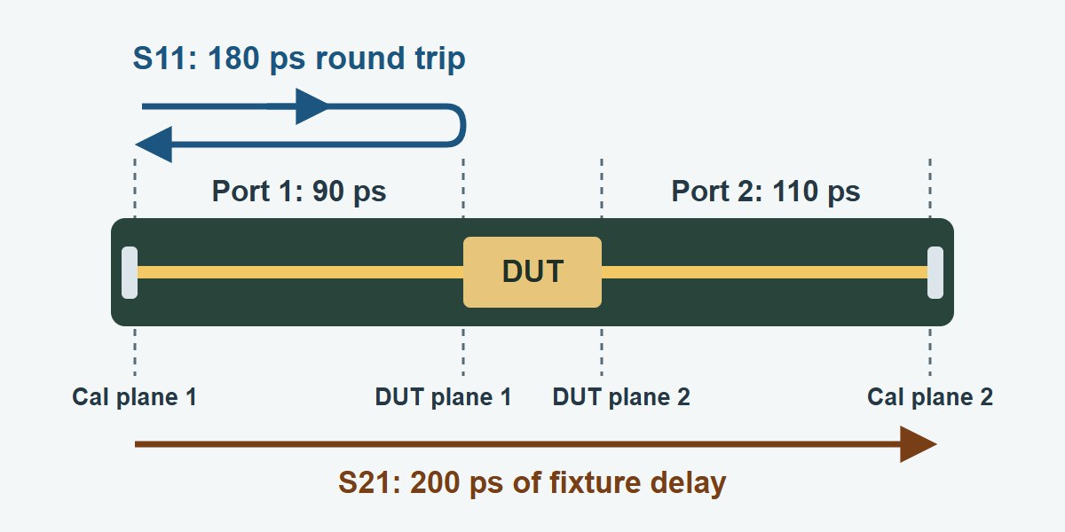
A useful sanity check: entering 180 ps for port 1 leaves 180 ps of excess round-trip correction. That is +64.8° per GHz of residual S11 slope in the example. If the corrected slope changes sign and is close to the original size, check for a factor-of-two error before changing the fixture.
VNA Electrical Delay vs. Port Extension vs. De-Embedding
Choose according to what must be measured. A display delay is useful for inspecting a trace; a port extension is a plane correction based on a line model; network de-embedding can remove fixture behavior that the line model cannot describe. They are not interchangeable.
| Method | When to use it | When to switch |
|---|---|---|
| Electrical delay | Check one trace for non-linear phase. | You need to move a shared reference plane. |
| Port extension | Move the plane along a matched line. | The check short ripples or the phase slope varies sharply. |
| Network de-embedding | Use validated fixture networks to remove mismatch, loss and delay. | The model is unreliable or you can calibrate at the DUT plane. |
Validate at the same device plane regardless of method. For a simulation deliverable, too much delay removal can make the response arrive before its defined time origin. See the S-parameter causality guide for how to tell an origin error from finite-band ringing or time wrap.
Manual Port Extension: Verify the Phase Slope First
- Define the measurement first. Mark the coax calibration planes and DUT planes on the fixture drawing. Keep the sweep band, cable position, calibration settings and raw traces in the record.
- Measure a known reflection at the intended DUT plane. Unwrap the phase over usable points and account for the standard’s own phase if the manual method supports it. Do not fit across an unexplained notch, wrap or abruptly changing slope.
- Set the one-way delay on the correct port. Use the actual unit, such as ps rather than ns. If converting a physical length, use the line’s propagation velocity, not the speed of light in air; for a dispersive line, check that a constant delay is acceptable over the band.
- Start with delay only. Compare raw and corrected phase and magnitude at identical sweep settings. If magnitude moved, check whether loss compensation or another operation is enabled. Then verify with a different standard.
Automatic Port Extensions: When an Open or Short Is Good Enough
On the applicable Keysight implementation, the automatic function estimates delay from an open, a short or both, with an optional loss fit. It assumes an ideal standard in this operation. A populated footprint is not an open. Even an unpopulated footprint can have fringing capacitance; a short with a long return loop adds inductance. A seemingly clean fit can include the electrical length of the standard itself.
Use standards with reproducible geometry at the intended device plane. Record the open and short estimates before averaging or accepting the result. If they differ enough to exceed your phase error allowance, inspect the termination geometry and launch mismatch, or change the fit band with justification and verify across the full required band. Do not use the same open both to fit and independently approve the correction.
Loss Compensation: What the VNA Can and Cannot Correct
For an ideal matched-line example with 0.18 dB one-way fixture loss at port 1 and 0.25 dB at port 2 at 3 GHz, the correction is +0.43 dB to S21 and +0.36 dB to S11. Those sums explain a line loss adjustment; they are not fixture specifications. A mismatched launch can interact with the DUT reflection. A smooth loss curve cannot cancel that interaction, even if it makes the average amplitude look right.
Keep the loss fit disabled unless you can verify its improvement separately. If the corrected open or short shows substantial magnitude ripple around its expected response, investigate the fixture mismatch, standard and calibration before using the data. Avoid accepting a trace simply because an instrument option shifted every sample below 0 dB. That does not show that the two-port network is physically correct.
VNA System Verification: A Check Standard You Did Not Fit
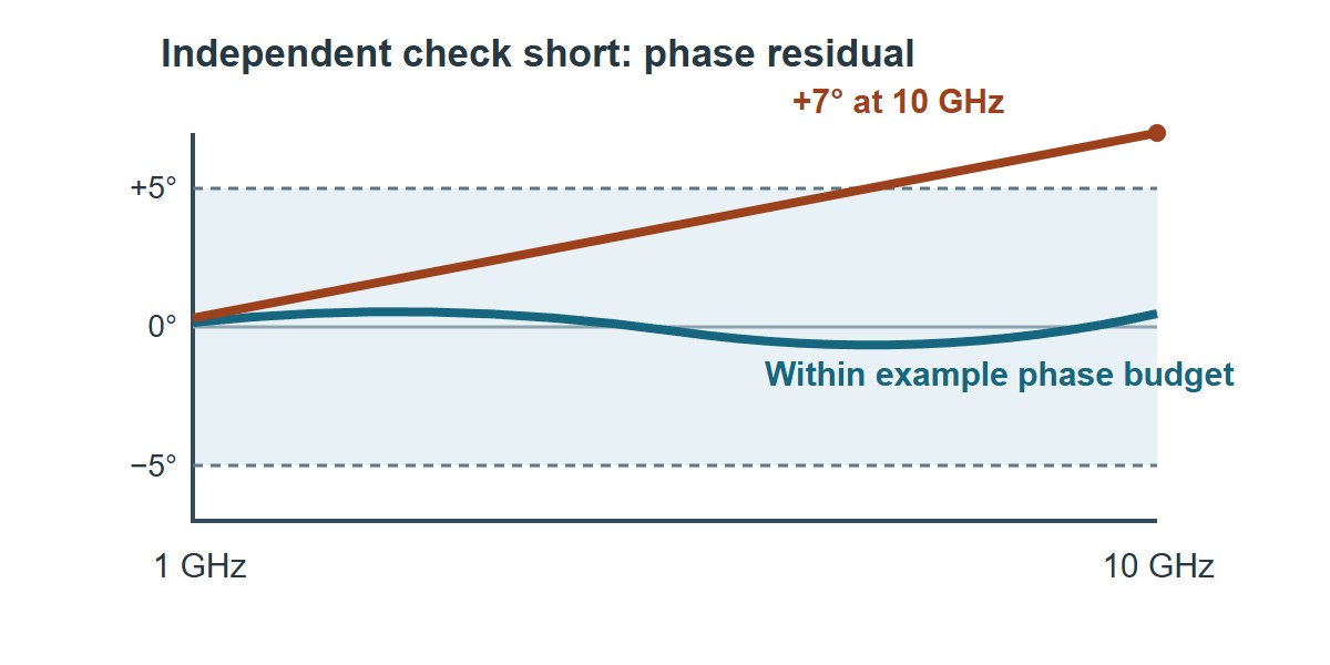
Use the following worksheet after changing a reference plane. Fill in the band, known standard, separate limits for phase and amplitude, and the measured residual for each. Use an independent check short or load for reflection and a characterized verification line or through for transmission, as appropriate. A load can check reflection magnitude and residual match; its small reflection makes it a poor phase reference. A nonzero-length through must be compared against its known delay, not a flat zero-degree trace.
| Field | Example | Decision |
|---|---|---|
| Band and test | 1–10 GHz; independent short at port 1 DUT plane. | Save raw and corrected S11 and the short model. |
| Phase residual | Example limit: ±5°. Example result: +7° at 10 GHz. | Hold data. Refit or change method and verify again. |
| Other checks | Enter magnitude error and reconnection spread. | Do not accept on phase alone. |
If the entire ±5° phase allowance at 10 GHz were assigned to a pure delay error, S21 would permit only 1.39 ps of total delay error; S11 would permit 0.694 ps of one-way error. In a real budget, allocate part of the allowance to the calibration, standard and repeatability as well. The example is not an IPC acceptance limit; use the applicable drawing or agreed measurement procedure.
PCB Test Fixture: Where Port Extension Is Useful
Filter coupon: preserve the filter, remove the feeds
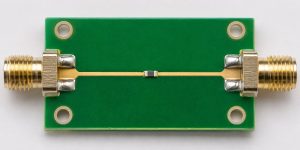
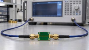
Put the DUT planes at the filter’s port pads when comparing against a pad-referenced model. Determine the one-way delay of both feed sections. Verify with a known through or line before installing the filter. Accept the result only if the reference agrees with phase and loss budgets and the measured filter passband, stopband and group delay meet the project limits. Do not fit the fixture correction on the filter passband and then use the same fit as proof of filter delay.
PCB antenna: report at the feed you intended to tune
If the matching network is specified at its antenna feed, set the port 1 plane there, leaving the antenna and intended matching elements in the measured network. Verify with a separate short or load on a matching coupon, then check the frequency and depth of S11 minima and the usable band against the antenna requirement. A delay-only correction rotates the impedance display but cannot improve return-loss magnitude. If the connector is the specified product test plane, measure and report there instead.
Mismatched connector launch: distinguish the two failure modes
If the launch is itself the product feature under test, leave it inside the DUT boundary and compare to the connector-plane mask. If it is only a fixture and its ripple dominates the error budget, validate a fixture model or calibrate at a closer plane. In both cases retain raw and processed files, calibration identifiers, port directions and the verification result. If there is no check standard or equivalent validation, label the trace as diagnostic instead of releasing it as verified device data.
VNA Port Extension FAQs
Is port extension a replacement for SOLT calibration?
No. Calibrate first at an accessible plane. The extension then moves the reference through a section modeled separately; it does not solve the same systematic error terms as calibration.
Does port extension improve S11?
Delay-only correction changes phase, not magnitude. A reported magnitude change may come from enabled loss compensation or a different processing step, not an improvement of the hardware.
Can port 1 and port 2 use different delays?
Yes. Fit and record each separately. S21 and S12 cross both sections; each reflection uses its own section twice.
Why did my open and short give different delays?
The standards may be nonideal or located at different planes, or fixture mismatch may change the fit. Inspect the geometry and compare the estimates against the phase budget.
Can I use the delay shown by a NanoVNA directly?
Check the software and firmware manual for whether the displayed value or setting represents one-way line delay, round-trip delay or a trace-level phase correction. Verify it on a known length before transferring settings between instruments.
Should I average delay across a wide band?
Only where the fixture behaves as the assumed model and the independent reference meets the required full-band residual. A narrower fitting band does not by itself validate operation outside it.
Does time gating solve the same problem?
No. Gating suppresses selected time events in the processed response. Port extension moves the reporting plane; it does not selectively remove an echo. Keep the unprocessed data either way.
What goes into the Touchstone delivery notes?
Include the original and output planes, port order and reference impedance, sweep band, one-way delay by port, loss and other processing settings, and the verification evidence.
Technical References
- Keysight: Comparing the VNA Delay Functions — reflection and transmission factors, phase-slope limits and fixture mismatch.
- Keysight: Port Extensions — manual delay, loss adjustment and automatic open/short procedure.
- Keysight: De-Embedding and Embedding S-Parameter Networks Using a Vector Network Analyzer — application note 5980-2784, printed page 12 and Figure 13.
Custom RF PCBs With Stackup and Test Coupon Review
Ordering an RF PCB or a separate test coupon? Send EBest Circuit your intended stackup, controlled-impedance targets, launch drawing and test-plane locations before releasing the fabrication data. An early review gives your fabrication and lab teams the same geometry to reference when they compare board and coupon results.
Request an RF PCB quote from EBest Circuit with your Gerbers or ODB++, quantity and required delivery date.