

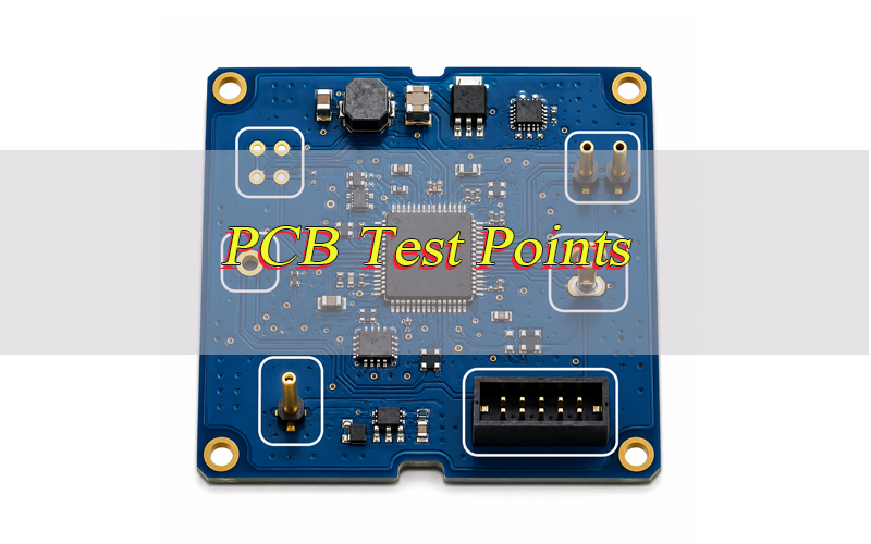
PCB test points give engineers and manufacturers a safe, repeatable place to measure signals, power, ground and circuit behavior. They help verify whether a PCB works as designed before it moves into assembly, shipment or final product use.
In PCB manufacturing, small test pads can have a large impact on inspection efficiency. Good access points reduce debugging time, improve ICT and flying probe accuracy, and lower the risk of damaging components during manual measurement. For buyers, well-designed PCB test points also reduce mass production risk and make prototype validation more reliable.
What Is the Test Point in PCB?
A test point in PCB is an exposed electrical access location used for measurement, debugging, programming or production testing. It is usually connected to a specific net, such as power, ground, reset, clock, signal line or communication interface.
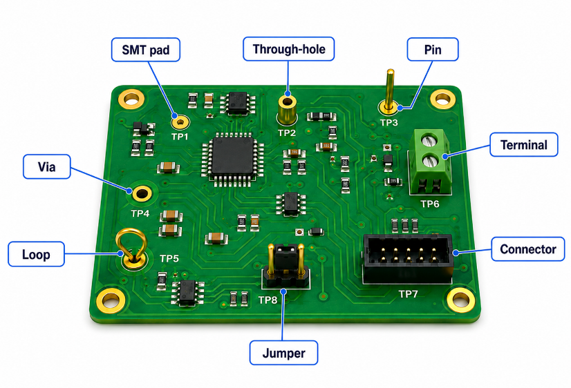
PCB test points can be round pads, square pads, vias, pins, loops, terminals or connector-based access points. Their purpose is to let probes or test fixtures contact the circuit without touching delicate component pins. This protects components and improves test repeatability.
In real production, a test point is not only a small copper pad. It is part of the full DFT review process. A good test point helps engineers check continuity, voltage, waveform, current path and possible manufacturing defects before the board enters final assembly.
What Are the Different Types of PCB Test Points?
Different types of PCB test points are selected according to the test method, PCB space, contact strength and production stage. Some are designed for automated testing, while others are better for manual debugging, oscilloscope measurement, firmware programming or field service. The right type should match the probe, fixture and inspection purpose, not only the available layout space.
- SMT test pads: Flat exposed pads used for ICT, flying probe testing and manual probing.
- Through-hole test points: Plated holes used for stronger probe contact, test pins or repeated measurement.
- Via test points: Exposed vias used as compact access points when PCB space is limited.
- Loop test points: Raised loop-style points used for oscilloscope clips, hook probes and manual debugging.
- Pin test points: Soldered PCB test point pins used for repeated bench testing or engineering validation.
- Terminal test points: Fixed terminal-style access points used when stronger mechanical connection is required.
- Connector test points: PCB test point connectors used for programming, functional testing, field service or repeated signal access.
- Jumper test points: Mount PCB test point jumpers used for configuration, isolation, debugging or optional circuit connection.
How Do PCB Test Points Work During Testing and Debugging?
PCB test points work by giving a probe direct electrical contact with a selected circuit net. The tester then measures voltage, resistance, continuity, waveform, frequency or signal response.
During manual debugging, engineers often use a multimeter, oscilloscope or logic analyzer. For example, a PCB oscilloscope test point may be used to observe clock signals, switching nodes, reset lines or communication waveforms. A nearby ground point also helps improve signal accuracy.
During automated testing, pogo pins or flying probes contact test points on PCB one by one or in groups. The test system compares the measured values with preset limits. If an open circuit, short circuit, wrong component, soldering defect or abnormal voltage appears, the system can identify the failure more quickly.
As a result, test points improve both engineering analysis and production quality control. They make fault isolation easier, reduce repair time and help prevent defective boards from moving into the next production stage.
What Is the Standard Size of a PCB Test Point?
There is no single universal PCB test point size, but common production pads are usually designed around 0.8 mm to 1.5 mm when board space allows. Smaller pads may work, but they increase probing difficulty and false test risk.
For ICT or flying probe testing, the suitable PCB test point size depends on fixture tolerance, probe tip diameter, board density and manufacturing capability. A PCB test point minimal diameter around 0.4 mm may be possible for some flying probe applications, but it is not the best choice for stable mass production.
| Type | Common Size | Use Case |
|---|---|---|
| Manual pad | 1.0–1.5 mm | Debugging and repair |
| ICT pad | 0.75–1.0 mm | Fixture testing |
| Flying probe pad | 0.4–0.8 mm | Prototype and small batch |
| Through-hole point | 0.8–1.2 mm hole | Probe or pin access |
| Loop point | Project dependent | Oscilloscope clip |
When space allows, a larger pad improves contact reliability, reduces fixture pressure sensitivity and makes inspection easier for engineers. In contrast, pads that are too small may increase false rejects, fixture adjustment time and quality control uncertainty.
What Is the Spacing for PCB Test Points?
PCB test point spacing should be large enough to prevent probe shorting, fixture collision and solder mask bridge issues. In many practical layouts, 1.27 mm to 2.54 mm spacing is used depending on probe type and board density.
Tighter spacing may be accepted on dense boards, but it increases manufacturing and testing risk. For production-friendly design, PCB test point clearance should also consider nearby components, vias, copper pours, solder joints and board edge keepout. This helps the fixture contact the board safely and consistently.
| Item | Suggested Range | Notes |
|---|---|---|
| Pad-to-pad spacing | 1.27–2.54 mm | Larger is safer |
| Pad-to-component clearance | 1.27 mm or more | Avoid probe interference |
| Board edge distance | 3.0 mm or more | Helps fixture support |
| Tall component clearance | Project dependent | Check probe angle |
| Mask opening margin | Fabricator dependent | Prevent covered pads |
Good spacing makes PCB test points easier to contact and lowers the chance of unstable readings during ICT, flying probe and manual inspection. It also helps reduce fixture cost because the test fixture does not need extreme precision to avoid adjacent pads.
How Should PCB Test Points Be Placed on a PCB?
PCB test points should be placed where probes can reach them easily without disturbing the circuit or damaging the board. Placement should follow the test plan, not leftover layout space.
- Place test points on important nets first, including power rails, ground, reset, clocks, programming pins and communication signals.
- Keep points away from board edges, mounting holes, tall components, connectors, shields and heatsinks.
- Put automated test points on one side when possible to reduce fixture cost and complexity.
- Add nearby ground access for oscilloscope measurements and sensitive signal checks.
- Avoid long stubs on high-speed or RF signals because they can affect signal integrity.
- Keep enough PCB test point clearance around each pad for probe travel and fixture tolerance.
Good test point placement PCB planning supports stable testing from prototype to mass production. It also helps buyers avoid redesign cost after the first sample build, especially when ICT, flying probe or functional testing is required for batch production.
How Do We Design Test Points in PCB Board?
PCB test points should be designed from the test plan before the PCB layout is finalized. A good design makes testing easier, reduces fixture cost and prevents mass production risk.
Step 1: Confirm the test purpose.
Decide whether the board will use manual probing, ICT, flying probe testing, programming, functional testing or repair inspection. Different test methods require different PCB test point size, spacing and access style.
Step 2: Select the critical nets.
Prioritize power rails, ground, reset, programming pins, clocks, communication lines, enable signals and key analog or digital nodes. Do not add test points randomly; every point should support a clear test purpose.
Step 3: Choose the right test point type.
Use SMT pads for automated testing, through-hole points for stronger contact, loop points for oscilloscope clips and connectors for repeated programming or service access. The PCB test point footprint should match the actual probe or fixture.
Step 4: Set proper size, spacing and clearance.
Use a pad size that the probe can contact reliably. Keep enough PCB test point clearance from nearby pads, vias, components and copper areas. Poor spacing can cause probe shorting, false failures and fixture alignment problems.
Step 5: Place test points in accessible areas.
Keep them away from tall components, shields, heatsinks, batteries, mounting holes and board edges. For automated testing, place test points on one side when possible to simplify fixture design and reduce fixture cost.
Step 6: Protect sensitive signals.
Avoid long stubs on high-speed, RF, clock or impedance-controlled traces. For oscilloscope measurement, place a ground point close to the signal point to improve waveform accuracy.
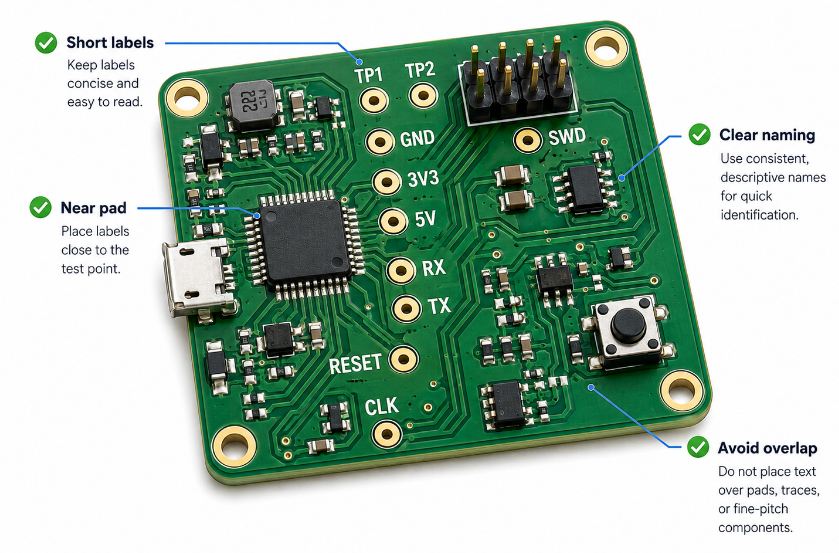
Step 7: Add clear markings and documents.
Mark test points with simple labels such as TP1, GND, 3V3, RESET, RX or TX. Keep the full net list in the test document or assembly drawing so engineers can identify each point quickly.
Step 8: Run DFT and DFM review.
Before Gerber release, check solder mask openings, pad exposure, probe access, spacing, fixture compatibility and test coverage. This step helps confirm that the test points are not only correct in layout but also usable in real PCB manufacturing.
How Are Test Points Marked on a PCB?
Test points are usually marked with short silkscreen labels such as TP1, TP2, GND, 3V3, 5V, RX, TX, SWD, RESET or CLK. Clear markings help engineers test the board faster and avoid wrong probing.
The label should be close to the pad but not printed over exposed copper, solder mask openings or fine-pitch component areas. For dense boards, short labels are better than long net names. The full test point list can be included in the fabrication drawing, assembly drawing or test document.
Consistent marking also supports repair and field troubleshooting. When multiple test points in PCB are crowded together, a clean naming system helps technicians quickly identify voltage rails, signal nets and programming access. This reduces human error during prototype debugging and production inspection.
How to Connect to PCB Test Points?
PCB test points can be connected by manual probes, oscilloscope probes, pogo pins, flying probes, hook clips, pin headers, terminals or test connectors. The connection method should match the test purpose and production volume.
Step 1: Identify the correct test point.
Check the silkscreen label, schematic, net list or test document before probing. Wrong contact may cause incorrect readings, short circuits or circuit damage.
Step 2: Choose the proper tool.
Use a multimeter probe for voltage, resistance or continuity checks. Use an oscilloscope probe for waveform testing. Use pogo pins, flying probes or bed-of-nails fixtures for production inspection.
Step 3: Confirm the ground reference.
For voltage and waveform checks, connect the ground lead to a nearby GND test point. A short ground connection gives more stable readings, especially when testing clocks, switching signals or analog circuits.
Step 4: Contact the pad carefully.
Touch the exposed pad, via, pin, loop or terminal with steady pressure. Avoid slipping into nearby components or adjacent copper. For small PCB test points, use a fine probe tip or controlled fixture.
Step 5: Apply the correct test condition.
Some checks require the board to be powered off, such as resistance or continuity testing. Voltage, waveform and functional tests usually require the board to be powered under controlled conditions.
Step 6: Use stable access for repeated tests.
For repeated programming, aging tests or field diagnostics, use PCB test point connectors, pins or terminals instead of hand probing small pads. This improves durability and reduces human error.
Step 7: Record abnormal readings.
If a test point shows unstable voltage, no continuity, wrong waveform or intermittent contact, record the net name, measured value and test condition. This helps engineers trace layout, assembly or component problems faster.
How to Check Test Points on PCB?
PCB test points should be checked before fabrication, after prototype build and before mass production. The goal is to confirm that every important test point is electrically correct, physically accessible and suitable for the selected test method.
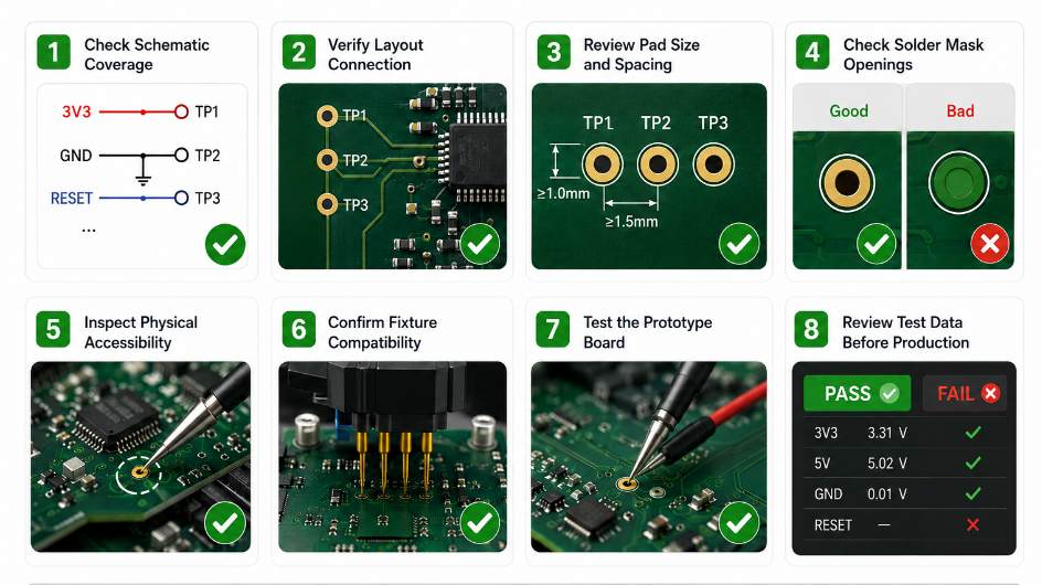
Step 1: Check the schematic coverage.
Confirm that important nets have test access, including power, ground, reset, clocks, programming pins and key communication signals. Missing critical nets can make debugging and fault isolation difficult.
Step 2: Verify the PCB layout connection.
Check that each test point is connected to the correct net. A test point on PCB is only useful when the net assignment is correct and the pad is not accidentally isolated by layout errors.
Step 3: Review pad size and spacing.
Measure the PCB test point size, pad-to-pad spacing and PCB test point clearance. Pads that are too small or too close may cause weak contact, probe slipping, shorting or false test failures.
Step 4: Check solder mask openings.
Make sure the test pad is exposed and not covered by solder mask. Covered pads cannot make stable electrical contact, even if they are visible in the PCB design file.
Step 5: Inspect physical accessibility.
Confirm that probes can reach the test points after assembly. Avoid locations blocked by tall components, shields, connectors, heatsinks, batteries, glue or mechanical parts.
Step 6: Confirm fixture compatibility.
For ICT or flying probe testing, check whether the probe size, travel direction, fixture pressure and board support match the layout. This is important for in-circuit testing test point requirements and mass production quality control.
Step 7: Test the prototype board.
Use the real probe, fixture or test cable to verify the first sample. This confirms whether the designed test points work under actual board tolerance, solder mask registration and assembly conditions.
Step 8: Review test data before batch production.
Before mass production, compare prototype test results with expected values. If unstable contact, false failure or access problems appear, revise the PCB test point guidelines before releasing the final production files.
What Common PCB Test Point Design Mistakes Should Be Avoided?
PCB test point design mistakes usually come from poor access planning, small pad size, weak spacing control and missing DFT review. These problems may not appear in the schematic, but they can cause false failures, slow debugging and higher fixture cost during real production.
- Using pads that are too small:
Very small PCB test points may save layout space, but they make probe contact unstable. In ICT or flying probe testing, small pads can cause probe slipping, weak contact and false rejects. For mass production, use the largest practical pad size allowed by the layout. - Placing test points too close together:
Tight spacing increases the risk of probe shorting between adjacent pads. It also makes fixture alignment harder. Proper PCB test point clearance should consider probe diameter, solder mask tolerance, nearby copper and board manufacturing variation. - Putting test points under components or mechanical parts:
A test point is useless if it is blocked after assembly. Avoid placing test points under connectors, shields, batteries, heatsinks, glue, tall components or enclosure contact areas. Always check accessibility after the full PCBA structure is assembled. - Ignoring ground access near key signals:
Oscilloscope measurement becomes less accurate when the ground reference is far away. For clocks, switching nodes, analog signals and communication lines, add a nearby GND test point. This helps reduce noise and improves waveform reading accuracy. - Adding long stubs to high-speed traces:
A poorly placed test point can create a stub on USB, Ethernet, RF, DDR or clock lines. This may affect impedance, signal integrity and EMI performance. For sensitive nets, keep the test point short, controlled and reviewed by layout rules. - Relying only on component pins for testing:
Probing IC pins or fine-pitch components increases the risk of bent leads, solder bridge damage and unstable readings. Dedicated PCB test points make testing safer and more repeatable, especially during repair, programming and functional inspection. - Forgetting solder mask openings:
A test point must expose copper or a suitable plated surface. If the pad is covered by solder mask, the probe cannot make reliable electrical contact. Always check Gerber files to confirm the solder mask opening before fabrication. - Using unclear or missing markings:
Unmarked test points slow debugging and increase the chance of probing the wrong net. Use simple labels such as TP1, GND, 3V3, RESET, RX or TX, and keep a full test point list in the test document or assembly drawing. - Mixing automated test access on both sides without review:
Double-sided test access can increase fixture cost and mechanical complexity. If ICT testing is planned, place PCB test points on one side where possible. If both sides are required, confirm fixture feasibility before PCB fabrication. - Skipping DFT review before Gerber release:
Many test access problems are found too late because the layout only passes electrical DRC. A DFT review should check test coverage, pad exposure, fixture access, spacing, labels and mass production test requirements before final release.
FAQs About PCB Test Points
Q1: Should PCB test points have continuity?
A1: Only PCB test points connected to the same net should have continuity. A GND test point should have continuity with other ground points, but it should not be shorted to a signal or power net. If two unrelated test points show continuity, check the schematic, net tie, jumper, resistor path or possible short circuit before approving the board.
Q2: Can a via be used as a PCB test point?
A2: Yes, a via can be used as a test point if it is exposed, reachable and large enough for the selected probe. However, a dedicated test pad is usually more reliable because it offers a flatter contact surface. If vias are used for testing, confirm solder mask opening, via plating quality and probe compatibility before production.
Q3: What is the best surface finish for PCB test points?
A3: ENIG is often preferred because it provides a flat and stable contact surface. HASL, OSP and immersion silver can also work, depending on cost, storage time and test frequency. For repeated probing, surface flatness, cleanliness and oxidation resistance matter more than simply choosing the lowest-cost finish.
Q4: Do all nets on a PCB need test points?
A4: Not every net must have a test point. Full access is helpful for ICT, but compact or cost-sensitive boards may only expose critical nets. At minimum, provide access to power rails, ground, reset, programming pins, clocks and key communication lines. The final decision should balance test coverage, board space and production risk.
Q5: Can PCB test points be placed on both sides of the board?
A5: Yes, but it should be decided carefully. Double-sided access may increase fixture cost, fixture complexity and test setup time. For automated testing, single-side access is usually more efficient. If both sides must be used, confirm component height, probe direction, board support and fixture pressure before releasing the PCB layout.
Q6: Why do PCB test points fail during production testing?
A6: Common causes include small pad size, covered solder mask, poor plating, wrong net connection, insufficient spacing, probe misalignment and blocked access after assembly. Sometimes the design looks correct in CAD but fails in the fixture. Prototype fixture validation helps catch these problems before mass production starts.
Q7: Are PCB test points useful for functional testing?
A7: Yes. Functional testing often uses test points to check power rails, enable signals, communication lines, programming pins and system response. These access points help confirm whether the assembled PCBA works under real operating conditions. Good test access shortens troubleshooting time when a board fails during final inspection.
Q8: Can test points affect signal quality?
A8: Yes, especially on high-speed or RF circuits. A test point can add capacitance, create a stub and disturb impedance if it is placed carelessly. For USB, Ethernet, RF, DDR or fast clock lines, keep the test point short and controlled, or use indirect testing through connectors or built-in diagnostics when needed.
Q9: What is the difference between a test pad and a test point connector?
A9: A test pad is a simple exposed copper area for probing, while a test point connector is designed for repeated cable, tool or fixture connection. Pads are cheaper and save space. Connectors are better for firmware loading, field service and repeated engineering tests. The right choice depends on test frequency and durability needs.
Q10: Should PCB test points be soldered?
A10: Flat SMT test pads are usually not intentionally soldered because they are designed for probe contact. Their surface should remain exposed and clean. Pins, terminals, loops and connectors may be soldered if they are part of the test access design. Avoid excessive solder on probe pads, as it may reduce contact consistency.
Q11: How many ground test points should a PCB have?
A11: The number depends on board size, circuit type and test method. A simple board may need only a few ground points, while a larger or mixed-signal board may need several. For oscilloscope testing, a nearby GND point is strongly recommended because it improves waveform accuracy and reduces measurement noise.
Q12: Can PCB test points be added after fabrication?
A12: It is possible to solder wires, expose vias or use component pads during emergency debugging, but this is not suitable for controlled production. Reliable test access should be planned before Gerber release. Adding test points after fabrication increases rework risk, slows testing and may damage the board during repeated measurements.
Q13: What documents help manufacturers review PCB test points?
A13: Useful files include Gerber files, drill files, schematic, PCB layout data, BOM, assembly drawing and test requirements. If ICT, flying probe or functional testing is planned, provide the target nets and expected test method. Complete documents help the factory review access, clearance, solder mask opening and fixture feasibility before production.
Q14: How can buyers judge whether a PCB test point design is production-ready?
A14: Buyers should check whether critical nets are covered, pads are exposed, markings are clear and the selected test method is feasible. The design should also consider fixture cost, board support and access after assembly. A production-ready design should pass both DFM and DFT review, not only electrical DRC.
Conclusion
PCB test points are small layout features, but they directly affect debugging speed, test accuracy, repair efficiency and production reliability. A good design should define the correct access type, pad size, spacing, clearance, solder mask opening, marking method and test process before PCB fabrication begins.
For engineering teams, the best approach is to plan test access early, protect sensitive signals and match the test point design to ICT, flying probe, functional testing or manual debugging needs. For procurement teams, choose a manufacturer that can review DFT details, support prototype validation and control mass production quality.
EBest Circuit is a China source factory providing custom PCB fabrication and PCBA assembly with global delivery support. If you need PCB test point design review, prototype production or batch manufacturing support, send your Gerber files, BOM and test requirements to sales@bestpcbs.com for a fast quotation.
You may also like


Tags: pcb test points rules, pcb test points size, test points on pcb, types of pcb test points