PCB manufacturing PCB manufacturing
Home > Blog

Pyralux

Dupont Pyralux LF0111 Bond Ply for Multilayer Flex PCBs
Wednesday, November 4th, 2026

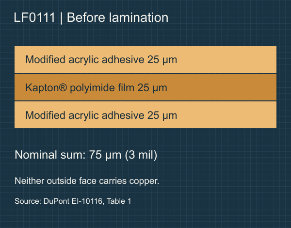
Dupont Pyralux LF0111 bonds two etched circuit layers together. It consists of a 25 ”m KaptonŸ polyimide film with 25 ”m of B-staged modified acrylic adhesive on each side. The two adhesive faces fill around the facing copper patterns during lamination, while the central film provides a continuous dielectric barrier. The copper belongs to the adjoining circuit layers; LF0111 itself contains no foil.
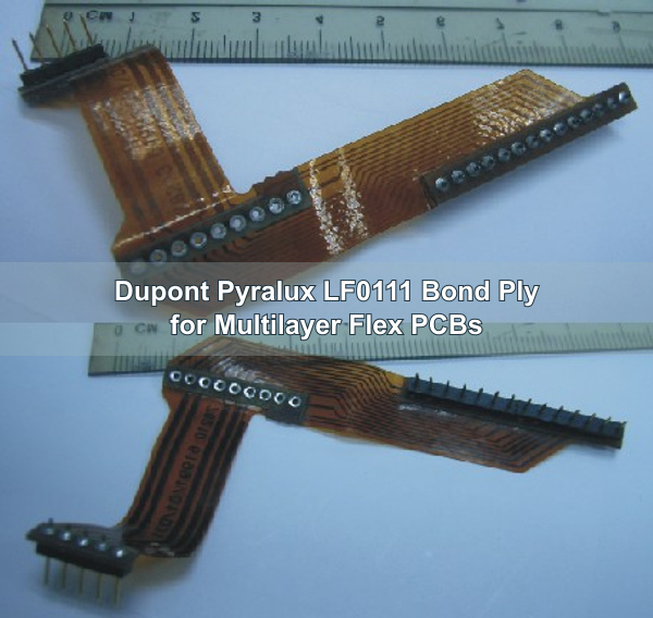
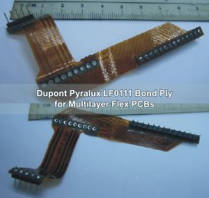
Flex circuit with component termination areas joined by a flexible section

Where Does LF0111 Go in a Flex PCB Stackup?

Place LF0111 between two patterned faces that need to be bonded and electrically isolated. In a multilayer PCB, each adhesive face contacts a separate circuit layer. That lets one bond ply encapsulate both etched patterns. A copper-clad core such as Pyralux LF8515R serves a different purpose: it supplies foil for forming traces.

For a rigid-flex board, mark the areas where the layers must be bonded and any area intended to flex with separate, unbonded leaves. Extending the bond ply across that free-flex region changes how the leaves move. A layer list alone cannot show where the bond boundary falls; put the outline on the mechanical drawing.

What Are the LF0111 Material Specifications?

DuPont identifies LF0111 by name in Tables 1 and 2 of its Pyralux LF Bond Ply datasheet (EI-10116). Table 1 describes the material construction. Table 2 gives typical laboratory measurements for LF0111. Use the test frequency and method alongside the value when comparing materials.

Feature or propertyLF0111 valueCondition or interpretation
Adhesive / Kapton / adhesive25 / 25 / 25 ”m (1 / 1 / 1 mil)Nominal incoming layers; count both adhesive faces.
Dielectric constant (Dk)3.6 at 1 MHz; 3.0 at 10 GHzIPC-TM-650 2.5.5.3 at 1 MHz; ASTM D2520 at 10 GHz.
Loss tangent (Df)0.020 at 1 MHz; 0.017 at 10 GHzSame respective test methods as Dk.
Adhesive flow0.05–0.10 mmTypical test result under IPC-TM-650 2.3.17.1.
Peel strength to copper1.8 N/mm as received; 1.6 N/mm after solderIPC-TM-650 2.4.9 on a prepared copper specimen.
Three incoming LF0111 layers, each 25 micrometers thick

How Does Adhesive Fill Around Copper Traces?

Before pressing, the raised copper traces touch the bond ply first. Between traces, the exposed substrate lies lower. As the adhesive heats and flows, some of it fills that relief. A sparsely routed area and an adjacent solid plane can therefore place different demands on the same adhesive face. The opposite face encounters its own copper pattern.

Show both facing artwork layers and the copper thickness at bonding. If an adhesive edge lies near an exposed pad, also dimension the area that must stay clear. The datasheet’s flow test gives a comparison value under a defined method. Using 0.10 mm as a universal pad setback would skip the effects of local copper distribution and the actual press process.
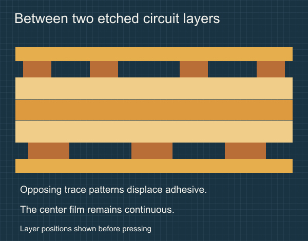
Facing trace patterns and both adhesive faces before pressing

How Thick Is LF0111 After Lamination?

Adding the three incoming layers gives a nominal 3 mil, or about 75 ”m using the rounded metric values in the datasheet. To see why that number cannot specify every finished gap, consider two locations on the same board: one where wide copper features face each other, and one where a trace faces an etched opening. The amount of adhesive needed beside the copper differs, as does the pair of surfaces from which you would measure.

If an impedance-controlled PCB requires a particular trace-to-plane spacing, identify those two copper surfaces on the cross-section. Give the target, tolerance and measurement location. The fabricator can then model the cured stackup and agree on a representative coupon. A nominal bond-ply thickness and a frequency-specific Dk are inputs to that review; neither establishes the impedance of a finished trace.

LF0111 Bond Ply vs LF0110 Coverlay

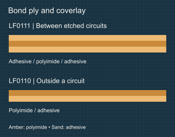
Both codes include Kapton film and modified acrylic adhesive. The decisive difference is the second adhesive face. DuPont’s LF coverlay datasheet, Table 1 identifies LF0110 as 25 ”m of film with 25 ”m of adhesive on one face. Substituting it between etched layers would leave one interface without the specified adhesive.

Drawing requirementLF0111 bond plyLF0110 coverlay
Layer sequenceAdhesive / polyimide / adhesivePolyimide / adhesive
Where it belongsBetween circuit details that must bondOn an outside circuit face, with film facing outward
Nominal sum before pressing75 ”m (3 mil)50 ”m (2 mil)
Artwork to supplyBonded area, cutouts and any no-bond regionPad and contact openings, edge clearances
LF0111 has two adhesive faces and LF0110 coverlay has one

What Lamination Conditions Does DuPont List?

DuPont lists typical LF processing ranges of 182–199 °C part temperature, 14–28 kg/cmÂČ pressure (200–400 psi) and one to two hours at temperature. The dwell refers to time at part temperature. A press platen reaching its setpoint does not by itself establish that the center of the stack has reached the same temperature.

For example, the peel-test footnote specifies a narrower setup: 182 °C, 200 psi and one hour, bonded to the treated side of 1 oz rolled-annealed copper. That footnote explains the peel specimen. The manufacturing cycle for a different layup should be qualified for that stack, copper surface and press equipment.

How Can You Check the Bonded Interface?

Choose a section through a feature that exercises the bond: for example, a broad copper region next to isolated traces or the edge of a cutout near a pad. A cross-section there can show whether adhesive filled the trace shoulders, whether a void remains, and whether material entered a keep-clear area. Mark the inspection location before lamination so the sample corresponds to the feature of interest.

If the application requires a peel test, define the specimen, foil treatment, conditioning and acceptance limit separately. A passing cross-section does not supply a peel-force result. Likewise, a datasheet peel value for treated copper does not verify bonding to a different surface on a finished board.

How Should LF0111 Be Stored?

DuPont specifies original packaging, 4–29 °C and less than 70% relative humidity. Keep the material dry and protected and avoid freezing. Preserve the package label so the material code, batch and quantity can be tied to the production job.

The datasheet ties its stated two-year warranty period to the date on the Certificate of Analysis, subject to the storage conditions. For material transferred from a partial roll, retain the original lot reference and handling record. Warehouse receipt date alone does not establish the certificate date or the roll’s storage history.

What Affects the Price of an LF0111 Flex PCB?

An LF0111 roll price and the price of a finished circuit cover different things. When we estimate board cost, we look at how many circuits fit on a production panel. A narrow bonded strip on each finished board can still require a panel-sized sheet during processing. The bonded outline, number of bonded interfaces, ordered board quantity and any sectioning or test coupons affect how much material and production work are needed.

For a prototype run, the same cross-section coupon costs more per delivered board when fewer boards share the panel. For a repeat run, compare the approved material code, coupon requirements and quantity with the previous order before using its unit cost. Confirm availability for the order. A datasheet listing alone does not establish stock, lead time or a current unit price.

How Should LF0111 Be Called Out on a Drawing?

A material note for Dupont Pyralux LF0111 can read: “Bond L2 to L3 using Pyralux LF0111 bond ply, nominal 1 mil modified acrylic / 1 mil Kapton / 1 mil modified acrylic. Bond only within the outline shown on mechanical layer BP1.” Replace the example layer names with the actual drawing references. Give the finished dielectric spacing separately wherever the design controls it.

Send with the drawingDecision it supports
L2 and L3 artwork plus copper thickness at bondingReview adhesive demand around facing traces and planes.
Dimensioned bond-ply outline and keep-clear areasLocate openings, rigid-to-flex transitions and free-flex leaves.
Critical spacing with tolerance and inspection locationDefine the feature the finished board must meet.
Order quantity, lot traceability and substitution policyCheck material availability and quote the approved build.

At EBest Circuit (Best Technology), we can review the proposed layer pair, the bonded outline and the areas that must remain free to flex. Send the stackup, copper files and mechanical drawing to sales@bestpcbs.com for a manufacturing review and quotation.

You may also like

DuPont Pyralux LF8515 Stackup and Copper Specifications
Wednesday, November 4th, 2026

DuPont Pyralux LF8515 is a flex-circuit material callout that needs a complete copper specification. For LF8515R, DuPont lists œ oz/ftÂČ rolled-annealed copper on each side, a 1 mil KaptonÂź polyimide core and 1 mil of modified acrylic adhesive on each face of the film. The 1 mil film entry alone does not give the distance between the copper layers. That distinction matters when a replacement core has to fit an existing connector or preserve a controlled-impedance trace.

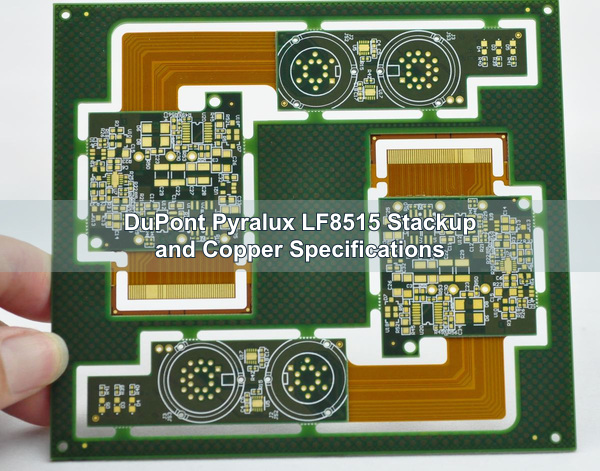
Rigid-flex circuit panel with patterned flex sections between rigid areas

Where Is LF8515R Used in a Flex PCB?

LF8515R supplies the two copper foils that a fabricator patterns into circuits. A designer can use both faces for routing, or use one face for signal traces and the other for a return path. The inner film insulates the two conductors. A connection between faces requires a designed interconnect, such as a plated hole.

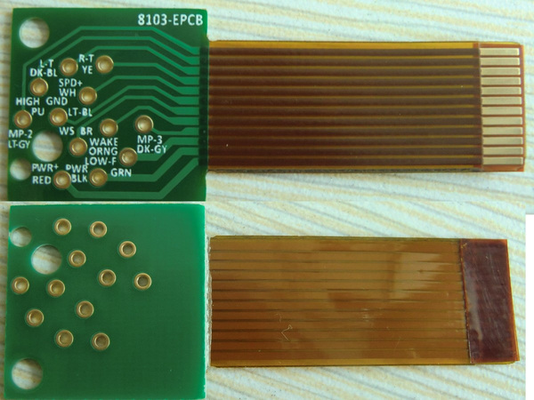
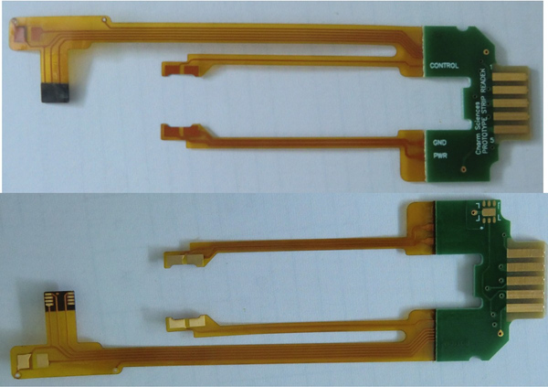
In a rigid-flex circuit, the flex core can run through a rigid component area and continue into a thin connecting tail. The FR-4 laminate in the rigid area adds support there. A drawing should identify where that rigid buildup ends and where the exposed flex begins. The product photographs show examples of these features; the material grade of the pictured circuits is unspecified.

Which DuPont Datasheet Lists LF8515R?

Use Table 2 of DuPont publication H-73244 (September 2002) for the exact LF8515R row. Its heading identifies double-sided copper-clad products. The copper column gives weight per unit area, while the adhesive and Kapton columns give thickness. Reading across the same row avoids accidentally using a single-sided construction from Table 1.

DuPont’s March 2020 LF copper-clad laminate datasheet, EI-10117 explains foil suffixes and lists standard offerings. LF8515R does not appear in those standard tables. The older row establishes the documented construction. For a new order, obtain current confirmation of the complete code, available sheet size and lot documentation before committing the build.

LF8515R Material Specifications

LF8515R featureNominal value in H-73244How to use it
CladdingDouble-sidedAssign a copper artwork layer to each face.
Copper on each faceœ oz/ftÂČ (153 g/mÂČ), rolled-annealedSpecify as starting foil. State any finished copper requirement separately.
Modified acrylic adhesive1 mil (25 ”m) on each faceInclude both bond lines when estimating conductor separation.
Kapton polyimide film1 mil (25 ”m)Count the center film once.
IPC entry in the historical rowCertified to IPC-4204/1 at publicationAsk for the current material lot’s certificate if the order requires it.

How Are the Five Layers Arranged?

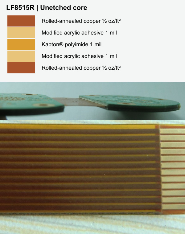
Read the unetched core from the top down: copper, adhesive, Kapton film, adhesive, copper. Both adhesive layers are inside the laminate. After etching, the remaining copper traces still rest on their respective bond lines. A drawing that shows copper directly against the film on either face describes a different construction.

LF8515R copper, adhesive and film sequence above examples of rigid-flex features

How Thick Is the Finished Flex Circuit?

Consider a nominal estimate before etching. The dielectric between foils is about 3 mil: 1 mil of adhesive on each side plus 1 mil of polyimide. Using the datasheet’s rounded metric values gives about 75 ”m. With nominal 18 ”m half-ounce copper on each face, the example bare core totals about 111 ”m. These are layer sums; thickness tolerances and measurements on a supplied lot are separate matters.

For a connector tail, specify the finished thickness and tolerance where the contacts engage. A reading over coverlay, a reading on an exposed contact and a reading over a stiffener can differ on the same part. Mark the measurement zone on the drawing and identify any plating, coverlay and stiffener included there.

Flexible contact tail with exposed fingers next to the supported rigid section

Does the Flex Stackup Need a Separate Coverlay?

Etching leaves copper on the outside faces of the core. If traces need insulation or environmental protection, specify the coverlay separately and draw its openings around contacts, pads and test points. The adhesive inside LF8515R cannot protect exposed traces. Conversely, an LF coverlay code in a bill of materials does not identify the copper-clad core.

At a connector, an opening that is too short can cover part of the mating contact. Show the opening edge relative to the contact area and dimension the stiffener on its own layer. That gives the fabricator two independently checkable features.

What Determines the Bend Radius?

A one-time installation fold and a tail that moves on every operating cycle pose different design problems. For an installation bend, show the installed radius and whether the bend will be reopened during service. For repeated motion, also specify the travel, direction and target number of cycles so the finished construction can be evaluated under those conditions.

The R suffix identifies rolled-annealed foil. It does not establish a cycle rating. A bend that starts at the stiffener edge or passes through a plated hole concentrates strain differently from a bend through a uniform tail. Mark the bend zone relative to these features on the mechanical drawing.

Two rigid-flex circuits with long flex branches and rigid connector ends

Which Dielectric Data Can You Use for Impedance?

For an impedance-controlled PCB, start with the signal layer, its reference conductor and the dielectric between them. A trace over the opposite foil sees the polyimide and both acrylic layers. Entering only the 1 mil film as the separation would model a different circuit. Copper coverage on the reference face and the coverlay above the trace also matter.

EI-10117 Table 3 identifies LF9110R as its test product. Its dielectric constant and loss values at the listed frequencies are typical for that specimen. For an LF8515R design, request construction-specific modeling inputs at the operating frequency, then agree on trace geometry, impedance tolerance and coupon verification with the fabricator.

LF8515R vs LF8510R

Historical constructionLF8515R · Table 2LF8510R · Table 1
Copper-clad facesTwoOne
Starting copper per clad faceœ oz/ftÂČ RAœ oz/ftÂČ RA
Kapton film / adhesive per clad face1 mil / 1 mil1 mil / 1 mil
Consequence for artworkCopper available for two patterned facesNo reverse-side foil for a second circuit or reference plane

A drawing with a signal on the front and a continuous return on the back cannot use LF8510R unchanged. The shared film thickness and copper weight would pass a superficial comparison, yet the return conductor would be missing. Check the face count before comparing the finer details of an alternative.

What Qualifies as an LF8515R Equivalent?

Ask the supplier for a cross-section and data sheet for the proposed code. Compare both foil types and weights, both bond lines, center film, dielectric thickness and the tolerance that matters to the assembly. A thinner adhesive can change trace-to-plane spacing even if foil weight and film thickness match. An adhesiveless laminate changes the dielectric construction even when its overall thickness looks close.

Identify what must be rechecked for the particular design. A connector interface needs a finished-tail thickness check. An impedance-controlled pair needs an updated stackup model. A moving tail may need a bend test on representative circuits. Obtain the design owner’s approval for the named substitution before production.

How Should LF8515R Be Specified on a Drawing?

A usable example for a legacy DuPont Pyralux LF8515 drawing is: “Flex core: Pyralux LF8515R, double-sided, œ oz/ftÂČ RA starting copper each face, 1 mil Kapton film, 1 mil acrylic adhesive each face. Any material substitution requires written approval.” Add the finished copper and thickness requirements where the design depends on them. The example is a material note, not a finished-board acceptance specification.

Send with the PCB drawingWhat it resolves
Layer order and copper artwork for both facesIdentifies which nets or return planes use the reverse foil.
Coverlay openings, stiffener outline and connector toleranceDefines thickness and exposed copper in the mating area.
Bend location, radius and service dutyDistinguishes installation forming from repeated motion.
Approved material revision and substitution restrictionsDefines whether an alternative can be quoted for engineering review.

At EBest Circuit (Best Technology), we can review the flex and rigid regions together against your stackup. Send the fabrication drawing, copper artwork, quantity and material approval requirements to sales@bestpcbs.com so we can confirm the construction and check availability for your order.

You may also like