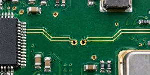
PCB propagation delay is the one-way time a signal takes to travel along a trace. For an initial estimate, multiply each trace segment’s length by its delay per unit length. Do not use one FR-4 constant for every layer: an outer-layer microstrip and an inner-layer stripline can have different delay rates even when their physical lengths match.
Suppose two signals must reach a receiver within a tight timing window. Equal lengths can look good in the PCB editor while the actual paths have different electrical delays. The useful comparison is in picoseconds at agreed reference planes, not just millimeters.
pcb propagation delay formula
For a uniform, low-dispersion transmission line, estimate the one-way delay as t ≈ L√εeff/c. Here L is trace length, εeff is dimensionless effective relative permittivity, and c is about 299.792 mm/ns. The formula returns nanoseconds when length is in millimeters. For a route with several uniform structures, estimate each segment separately and sum the delays.
| Input | Unit | Use |
| L | mm | Length of each segment |
| εeff | None | Line model |
| Speed of light | mm/ns | 299.792 |
| Delay rate | ps/mm | Rate × L |
Texas Instruments’ high-speed layout guide uses effective permittivity when comparing microstrip and stripline. Its example is a specific stackup, not an FR-4 rule. The approximation here also does not include connectors, package delay or a separate delay contribution from a via or launch.
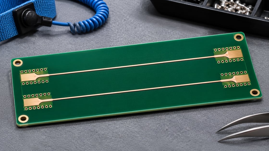
pcb propagation delay per mm
In the simple model, the delay rate is about 3.336√εeff ps/mm. Multiply a ps/mm value by 25.4 to express it in ps/in. Compare the rates using the same units and without rounding too early, especially when converting a short timing budget into allowable length mismatch.
| Model | ps/mm | ps/in |
| Microstrip (3.0) | 5.78 | 146.75 |
| Stripline (4.0) | 6.67 | 169.45 |
At 80 mm, those two example lines take approximately 462.2 ps and 533.7 ps. Equal lengths leave about 71.5 ps difference before package and transition contributions. These are modeled values, not universal measurements or recommended limits. In a real board, use the stackup and trace model agreed for the applicable layer, not the example’s assumed values.
fr4 pcb propagation delay
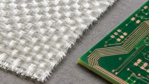
FR-4 is a material designation, not a single line velocity. A microstrip’s fields extend into more than one medium; laminate Dk, solder mask, trace width and height above the reference plane can all matter to the effective value. A homogeneous stripline approximation can use the surrounding dielectric value as a starting point, but mixed or asymmetric constructions still require a suitable model.
Microstrip vs. stripline for timing
When possible, route signals that must track each other through equivalent structures. If a layer change is unavoidable, ask for the relevant pressed thicknesses, material data and geometry so the solver can estimate delay by layer. Do not change to a different material solely to match the estimated velocity without also checking impedance, loss and manufacturing constraints.
pcb propagation delay calculator
Use a calculator only after choosing the units, reference planes and delay model. List every trace segment with its own delay rate; add a modeled or measured transition and package contribution if the timing budget includes those structures. Compare the complete path delays, not just their track-length totals.
- Decide whether the budget is for the bare board or the complete path to the device pins.
- Check the routing layers and divide mixed paths into uniform segments.
- Calculate with full precision, sum, then round the result for reporting.
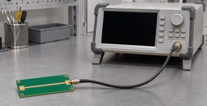
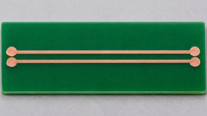
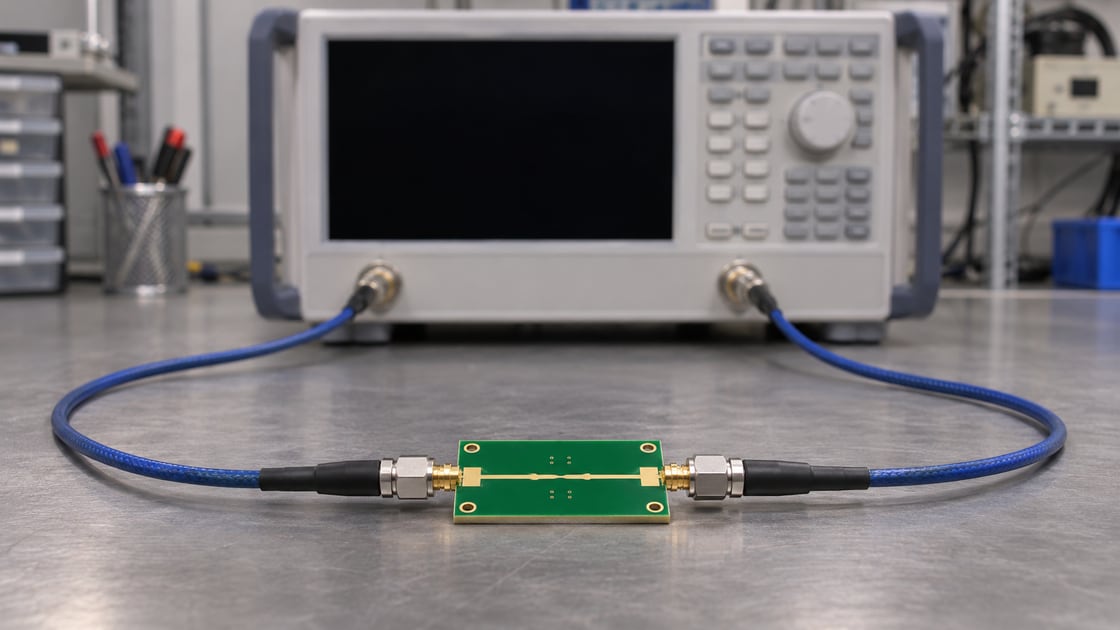
- If the margin is small, confirm the model against a suitable coupon or measurement with agreed reference planes.
For a 50 mm outer segment at 5.7775 ps/mm and a 30 mm inner segment at 6.6713 ps/mm, the estimated trace-only delay is about 489.0 ps. Compare that with 462.2 ps for the 80 mm all-outer route: the same total length still leaves about 26.8 ps of difference. Add transition effects separately if the budget includes them.
A reflection on a TDR time axis includes travel out and back; that interval is not the one-way flight time used here. The TDR fault distance guide covers the separate round-trip conversion. Keep its time convention out of an end-to-end timing budget.
FAQ
Is propagation delay the same thing as impedance?
No. Impedance describes the voltage-to-current relationship of a traveling wave in the line; propagation delay describes travel time. A routing change can affect both, but matching nominal impedance alone does not guarantee equal delay. Evaluate each against its own requirement using the actual routing structure.
Should I use 150 ps/in for every FR-4 trace?
Use a rule of thumb for a quick feasibility screen, not as a final budget for every layer. A mask-covered outer trace and an inner trace can have different delay rates. Ask for a stackup-specific model when the difference matters to receiver timing or routing decisions.
Does equal PCB length guarantee that two signals arrive together?
Only if the paths have comparable delay per unit length and comparable contributions from transitions and packages. A board editor can report equal trace lengths for electrically different structures. Compare estimated time from the relevant launch to the relevant receiver plane before declaring the paths matched.
Do I include the device package delay in length tuning?
Include it when the timing requirement is defined at internal device reference points or when the component vendor specifies a package compensation model. If the budget is only for board connections, report package delay separately. Define the endpoint convention before adding package length or time to PCB results.
How does a via enter a propagation-delay budget?
Its effect is not always captured by adding the board thickness to the planar length. The transition includes a three-dimensional field and may add phase, loss and reflections. Use a suitable via model or measurement when the margin is small, and state whether the estimate includes that contribution.
Can a faster rise time change which delay estimate I should use?
A faster edge contains more high-frequency content. If the channel is dispersive, a single low-frequency delay may not describe the edge shape or timing of interest. Use an appropriate bandwidth and measurement definition rather than treating the simple low-dispersion model as exact at every frequency.
Should I measure a connector and trace together?
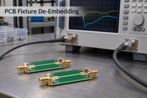
Measure them together if the requirement is for the complete interconnect. If you are trying to isolate the trace, use reference structures or agreed fixture removal to define the trace endpoints. Document which launch, cable or adapter contributions remain so another engineer can compare the results fairly.
How should I convert a skew budget into a length tolerance?
For two comparable uniform paths, divide the allowed time difference by the relevant delay per unit length. Do not use that shortcut across dissimilar structures without segment modeling. Apply package and transition allowances first if those contributions belong to the system’s budget.
Discuss Your Project
Send Best Technology the proposed stackup, routing layers, length or delay targets and timing reference points. Flag any planned layer changes or connector launches that need to be considered in the board review. Contact sales@bestpcbs.com.