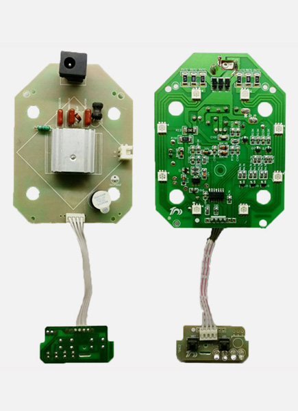
Need a custom power meter PCB manufacturer for precision assembly and urgent production? EBest Circuit provides custom PCB fabrication, component sourcing, SMT/THT assembly, and expedited manufacturing services for digital power meters, industrial measurement instruments, and electrical monitoring equipment. We support prototypes, small batches, and volume production based on customer-approved designs.
A reliable power meter PCB requires accurate sensing connections, suitable copper construction, and consistent assembly quality. Poor shunt connections, phase errors, or defective solder joints can affect measurement performance. How can you maintain measurement accuracy while meeting a tight production schedule?
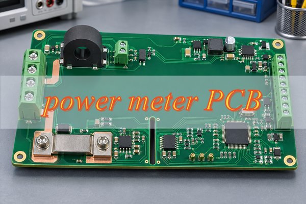
Which Power Meter PCB Configuration Is Suitable for AC, DC, and Three-Phase Applications?
The appropriate power meter PCB configuration depends on the electrical system, current-sensing method, measurement channels, and accuracy requirements. DC, single-phase AC, and three-phase applications require different circuit arrangements and manufacturing controls.
| Power Meter PCB Type | Typical Applications | Current-Sensing Method | Key Manufacturing Requirements |
| DC power meter PCB | Battery systems, DC power supplies, DC distribution equipment | Shunt resistor or Hall-effect sensor | Low-resistance connections, heat dissipation, stable sensing paths |
| Single-phase AC power meter PCB | Panel meters, AC equipment monitoring | CT, shunt resistor, or suitable current sensor | Phase matching, signal filtering, electrical insulation |
| Three-phase power meter PCB | Industrial power measurement, three-phase distribution | Multiple current-sensing channels | Channel consistency, insulation boundaries, connector alignment |
For three-phase power meter PCBs, engineers must also consider:
- Three-wire systems: The voltage measurement architecture depends on the available line-to-line voltages and selected metering IC.
- Four-wire systems: A neutral reference supports phase-to-neutral voltage measurement, depending on the equipment design.
- Channel matching: Voltage and current measurement channels need consistent component characteristics and appropriate filtering to limit gain and phase errors.
- Connector configuration: Terminal arrangements must match the electrical system, enclosure, and approved insulation requirements.
The selected measurement architecture should be confirmed before finalizing the PCB stackup, connector locations, and assembly files.
What Are the Critical Design Specifications for a Custom Power Meter PCB?
A custom power meter PCB must meet the required copper thickness, electrical insulation, material properties, mechanical dimensions, and signal-routing specifications. These requirements depend on whether the board carries load current or only processes measurement signals.
| PCB Specification | Engineering Reference | Design and Manufacturing Requirements |
| PCB layers | Commonly 2 or 4 layers | Match routing density, reference planes, and isolation boundaries |
| PCB material | FR-4 or specified laminate | Confirm thermal rating, dielectric properties, and operating conditions |
| Board thickness | 1.6 mm is a common option | Match enclosure dimensions, connector fit, and mechanical requirements |
| Copper thickness | 1 oz (35 μm) or 2 oz (70 μm) nominal copper foil | Size conductors according to actual current paths and allowable temperature rise |
| Trace width and spacing | Application-dependent | Meet current, routing, fabrication, and insulation requirements |
| Creepage and clearance | Determined by applicable insulation requirements | Consider working voltage, transients, pollution degree, and material properties |
| Surface finish | ENIG or lead-free HASL | Match component footprints and solderability requirements |
| Mechanical features | Custom outlines, slots, mounting holes | Maintain specified dimensions, terminal alignment, and isolation features |
Three details require particular attention before manufacturing:
- Current-carrying paths: A power meter rated for 20 A does not necessarily carry 20 A through PCB copper. If an external shunt or busbar carries the current, the PCB may handle only sensing signals. Conductor dimensions must follow the actual current and temperature-rise requirements, using the IPC-2152 adoption record where applicable.
- Electrical isolation boundaries: Copper clearances, plated holes, mounting features, and routed slots must preserve the approved insulation design. Safety-related dimensions should be clearly identified rather than inferred from the PCB layout.
- Manufacturing documentation: Provide the approved stackup, Gerber files, drill data, mechanical drawings, and critical tolerances. Terminal hole dimensions and isolation-slot locations deserve particular attention.
EBest Circuit manufactures power meter PCBs according to the approved fabrication data, with manufacturing concerns reviewed before production.
How Can Power Meter PCB Layout and Current-Sensing Methods Affect Power Measurement Accuracy?
PCB layout affects power measurement accuracy through unwanted resistance, electrical interference, grounding differences, and phase mismatch. The critical factors depend on whether the design uses a shunt resistor, current transformer, or Hall-effect sensor.
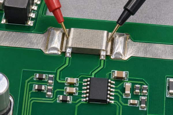
Shunt resistor measurement
A shunt produces a small voltage proportional to the measured current. Unwanted resistance can create a significant error when its voltage drop is included in the measurement path.
Consider a 2 mΩ shunt measuring 20 A:
- Expected sensing voltage: 20 A x 0.002 ohm = 40 mV.
- Additional connection resistance: 0.1 mΩ included in the measured path produces another 2 mV.
- Potential measurement error: 2 mV / 40 mV = 5%.
- Shunt power dissipation: 20 A x 20 A x 0.002 ohm = 0.8 W.
Kelvin sensing connections help prevent voltage drops in the main current path from entering the voltage measurement. The approved PCB layout must preserve the intended sensing points.
The shunt's power dissipation must also be considered because temperature changes can alter resistance and cause measurement drift.
Current transformer measurement
Current transformers introduce amplitude and phase characteristics that influence AC power measurement.
- Burden resistor: Its value and tolerance must match the transformer and metering circuit requirements.
- Phase matching: Voltage and current channel filtering must preserve the required phase relationship.
- Low power factor: At PF = 0.5, a 0.5° phase mismatch can produce approximately 1.5% active-power measurement error for sinusoidal signals under the stated conditions.
- Component consistency: Changes in burden resistance or filter components can introduce channel-to-channel differences.
Hall-effect sensing and signal routing
Hall-effect sensors can support AC or DC current measurement, depending on the device.
- Sensor characteristics: Offset, sensitivity, temperature drift, and nearby magnetic fields can affect accuracy.
- Noise control: Keep sensitive measurement traces away from switching nodes and high-current return paths.
- Reference paths: Follow the metering IC manufacturer's grounding and layout requirements. For a practical original-manufacturer example, review Analog Devices' AN-1562 layout guidance for an energy-monitoring circuit.
- Filtering and decoupling: Place components according to the approved circuit to minimize unwanted noise and signal distortion.
Accurate PCB fabrication and assembly preserve the specified sensing connections and component configuration, while measurement calibration remains part of the product validation process.
What Power Meter PCB Manufacturing Defects Can Cause Measurement Errors or Reliability Failures?
Incorrect precision components, defective sensing connections, soldering faults, and insulation defects can compromise power meter PCB accuracy and reliability. These problems require different manufacturing controls.
- Incorrect precision resistors: Wrong resistance values or temperature coefficients can alter measurement gain. Critical part numbers, values, and component tolerances must match the approved BOM.
- Poor shunt connections: Inconsistent soldering or damaged sensing terminals can introduce resistance or intermittent electrical contact. Kelvin connection geometry and critical joints require appropriate inspection.
- Insufficient through-hole solder fill: Large terminals and heavy copper areas absorb heat during soldering. Suitable thermal conditions are necessary to achieve acceptable wetting and solder fill.
- Copper and plated-hole defects: Opens, shorts, and inadequate hole plating can interrupt measurement or power connections. Bare-board electrical testing and fabrication inspection help identify these problems.
- Insulation defects: Incorrect slot dimensions, reduced conductor spacing, or damaged insulating surfaces can compromise isolation. Critical features must match the approved design.
- Unapproved substitutions: Replacing metering ICs, shunt resistors, or isolation components without engineering approval can change electrical performance or safety characteristics.
Manufacturing review should identify which connections, components, and insulation features require additional inspection before a production batch is released.
What Custom Power Meter PCB Manufacturing and Assembly Services Does EBest Circuit Offer?
EBest Circuit provides custom power meter PCB fabrication, component sourcing, precision assembly, and testing support according to customer-approved specifications. Customers can order bare PCBs or select an integrated PCBA manufacturing service.
Our services include:
- Custom PCB fabrication: Manufacture to the specified stackup, copper weight, laminate, surface finish, and mechanical requirements.
- Precision SMT assembly: Assemble metering ICs, ADCs, shunt resistors, precision passive components, QFN devices, and other specified SMDs.
- Fine-pitch assembly: Support small components, including 01005 packages and suitable fine-pitch BGA devices, subject to package and layout review.
- SMT/THT mixed assembly: Combine sensitive measurement circuitry with terminal blocks, connectors, and through-hole components.
- Full-turnkey PCBA: Coordinate PCB fabrication, approved BOM sourcing, component assembly, and agreed testing.
- Consigned assembly: Support customer-supplied metering ICs, precision resistors, or other critical components under an agreed material arrangement.
- Component sourcing: Procure parts against approved manufacturer part numbers and customer-authorized alternatives.
- Testing support: Arrange applicable electrical inspection, assembly inspection, firmware programming, and functional testing according to the project scope.
Free DFM check
EBest Circuit also provides a free DFM check for completed customer designs, including:
- Footprint fit: Review pad dimensions and component-footprint compatibility.
- Finished-hole fit: Check drill and plating allowances against through-hole component leads.
- Assembly access: Confirm component spacing and soldering accessibility.
- Stencil controls: Review aperture requirements for fine-pitch and bottom-terminated devices.
- Panel handling: Check panelization, tooling margins, and assembly support.
- Structure risks: Flag manufacturing concerns that could affect the approved construction.
Any proposed manufacturing changes are reviewed with the customer before implementation.
How Are Precision Components and High-Current Connections Assembled on Power Meter PCBs?
Precision power meter PCB assembly combines controlled SMT placement, suitable soldering conditions, and inspection of sensitive measurement components and high-current connections.
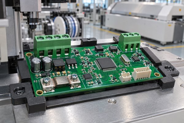
The assembly process follows the approved BOM, PCB construction, and component requirements.
- Verify released components: Start with the approved BOM, AVL, packaging, and moisture requirements. Match metering ICs, precision resistor values, manufacturer part numbers, packages, and polarity to the assembly data; quarantine any mismatch and record the material check before placement.
- Control solder-paste printing: Use the released stencil and the solder-paste specification for fine-pitch devices, small passives, and bottom-terminated packages. Inspect deposits with the agreed sampling or SPI plan so insufficient paste, bridging risk, or misalignment is corrected before components are placed.
- Place SMT components: Load the approved centroid file and orientation data, then place sensitive components without substituting part numbers or rotations. Verify first-article identities, polarity, and offsets before the batch continues because a wrong precision part can change measurement gain.
- Run the qualified reflow profile: Set the profile for the selected paste, component limits, board copper, and thermal mass. Confirm the recorded profile remains inside the approved process window; an unsuitable profile can create voids, opens, tombstoning, or heat damage.
- Assemble high-mass through-hole parts: Install the released terminal blocks, connectors, and larger components with soldering conditions appropriate to their leads and copper area. Inspect wetting and through-hole fill against the project acceptance criteria because heavy copper can draw heat away from the joint.
- Inspect and release the assembly: Compare the completed board with the approved drawings and first-article record. Check placement, polarity, visible joints, critical sensing connections, and selected hidden joints where required; document nonconformities before electrical or functional testing begins.
The most important process considerations are:
- Shunt resistors: Preserve the specified Kelvin terminals and sensing geometry. Soldering conditions should support stable electrical and thermal connections.
- Fine-pitch metering ICs: Control stencil design, solder-paste deposition, alignment, and reflow to reduce bridging and insufficient joints.
- High-current terminals: Large copper areas can draw heat away from solder joints. The soldering process must achieve adequate wetting and through-hole fill.
- Mixed-technology assemblies: Plan SMT and THT operations to maintain assembly access and avoid damaging installed components.
- Critical component handling: Follow specified moisture sensitivity, packaging, and temperature limitations where applicable.
For complex assemblies, EBest Circuit can review component footprints, soldering access, and inspection requirements before production.
How Can EBest Circuit Expedite Custom Power Meter PCB Manufacturing and Assembly?
EBest Circuit supports expedited power meter PCB manufacturing through early engineering review, material availability checks, and coordinated fabrication and assembly planning.
For qualifying standard bare-board prototypes, EBest Circuit's published quick-turn PCB fabrication options include:
- 1–2 layer PCB fabrication: Fastest published option of 24 hours.
- 4-layer PCB fabrication: Fastest published option of 48 hours.
These times apply to eligible bare-board fabrication orders, not complete power meter PCBA delivery. Actual availability depends on the approved specifications, materials, and production capacity.
How expedited PCBA orders are handled
- Engineering review: Complete Gerber files, BOM, placement data, and assembly drawings help identify manufacturing issues before production release.
- Material availability: Confirm stock for metering ICs, precision resistors, connectors, and other critical components. Customer-supplied parts may be evaluated when available.
- Parallel preparation: Coordinate PCB fabrication, stencil preparation, component procurement, and assembly documentation where practical.
- Priority scheduling: Assess available production capacity after confirming PCB complexity, order quantity, component readiness, and required processes.
- Testing preparation: Confirm firmware, test fixtures, measurement points, and acceptance criteria before assembly starts.
- Shipment planning: Evaluate the required factory completion date and delivery destination separately.
What can delay an urgent order?
- Special materials: Specialized laminates or nonstandard PCB construction can extend material and process preparation.
- Component shortages: Unavailable metering ICs or custom connectors can hold the assembly start.
- Open engineering questions: An incomplete BOM or unresolved fabrication issue prevents a controlled release.
- Extra test scope: Programming, fixtures, calibration, or functional-test requirements add preparation and execution time.
- Late revisions: Design changes after manufacturing release can invalidate tooling, materials, or inspection evidence.
The expedited lead time is confirmed after EBest Circuit reviews the actual order. Customers requesting urgent production should submit their quantity, required delivery date, and delivery location together with the approved manufacturing files.
How Does EBest Circuit Ensure Power Meter PCB Assembly Quality Before Delivery?
EBest Circuit supports power meter PCB quality through material verification, PCB electrical testing, assembly inspection, and customer-defined functional verification.
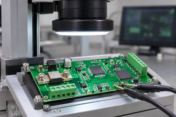
The inspection plan should address the defects most likely to affect measurement accuracy and connection reliability.
- Incoming component verification: Check approved metering ICs, precision resistors, connectors, and other critical BOM items.
- Bare PCB electrical testing: Identify opens and shorts against the approved electrical data.
- First-article inspection: Verify component identities, orientation, PCB revision, and assembly configuration before continuing the batch.
- SPI and AOI: Inspect solder-paste deposits, component placement, and visible soldering defects where applicable.
- X-ray inspection: Check selected hidden solder joints, including QFN or BGA connections, when required.
- ICT or electrical checks: Verify specified circuit connections and selected electrical conditions using agreed procedures.
- Functional testing: Test measurement responses, power-up behavior, communication interfaces, and firmware functions according to customer requirements.
Power measurement verification
For a DC power meter with a 0–20 A range, the customer may specify test points such as 0 A, 2 A, 10 A, and 20 A.
For AC measurement equipment, an approved test plan may include:
- Voltage and current accuracy at defined input levels
- Active-power accuracy under specified load conditions
- Power-factor verification at PF = 1 and PF = 0.5 where relevant
- Phase-channel consistency for applicable three-phase designs
- Firmware and communication checks where included in the assembly scope
Required acceptance information
- Test inputs: Define electrical inputs, loads, and measurement points.
- Pass limits: State permitted errors and pass/fail boundaries.
- Reference equipment: Identify instruments, calibration status, and any fixture requirements.
- Released configuration: Supply the approved firmware and measurement settings.
- Production records: Define required logs, traceability, and failure-handling procedures.
PCB inspection confirms manufacturing quality, while measurement calibration and equipment-level safety qualification require separately defined procedures.
For additional inspection information, see our PCB assembly testing services guide.
How Can You Reduce Custom Power Meter PCB Manufacturing Costs Without Compromising Quality?
Custom power meter PCB manufacturing costs can be controlled by matching fabrication requirements to the actual electrical design, maintaining an approved BOM, and reducing avoidable production changes.
The following measures can improve manufacturing efficiency:
- Optimize PCB layer count: Avoid additional layers when the approved routing, reference-plane, and isolation requirements can be met with a simpler stackup.
- Select copper weight appropriately: Heavy copper may be unnecessary if load current is carried through an external shunt or busbar.
- Standardize noncritical components: Use approved common components where electrical performance and safety are unaffected.
- Improve panel utilization: Review board outlines, panel arrangements, and tooling requirements to reduce manufacturing waste.
- Control component substitutions: Approve alternatives before procurement rather than introducing unexpected changes during assembly.
- Improve assembly access: Ensure connector locations and component spacing allow efficient soldering and inspection.
- Finalize documentation: Keep Gerber files, BOM, placement data, assembly drawings, and revision information consistent.
- Prepare test requirements early: Confirm firmware, fixtures, and acceptance criteria before production setup.
For repeat orders, stable specifications and controlled revisions reduce the risk of unnecessary process changes.
Critical sensing components, electrical insulation, and current-carrying requirements must remain within the approved engineering specifications.
How Does EBest Circuit Support Power Meter PCB Prototypes and Mass Production?
EBest Circuit supports power meter PCB projects from engineering prototypes to pilot production and repeat manufacturing, using customer-approved designs and assembly documentation.
Each production stage addresses a specific requirement.
Prototype manufacturing
- Fabricate samples: Build the PCB to the approved Gerber files and stackup.
- Assemble critical parts: Install the specified metering ICs, sensing components, and connectors.
- Capture build issues: Record fabrication or assembly concerns found during the initial build.
- Release validation units: Provide finished samples for customer electrical, thermal, and mechanical validation.
Pilot production
- Lock materials: Confirm component availability and the approved BOM revision.
- Verify soldering: Check the process for precision devices and electrical terminals.
- Establish inspections: Apply the agreed inspection and functional-testing procedures.
- Control configuration: Confirm firmware and production-document revisions.
- Close pilot issues: Record and resolve manufacturing issues before volume release.
Mass production
- Maintain revisions: Use controlled PCB and assembly files.
- Control procurement: Coordinate repeat purchases and approved substitutions.
- Repeat qualified processes: Apply the established assembly and inspection requirements.
- Preserve traceability: Maintain the agreed lot identification and production records.
- Review critical changes: Obtain approval before changing measurement components or processes.
The objective is to reproduce the validated design consistently across production batches, rather than introducing unapproved changes during manufacturing.
FAQs About Custom Power Meter PCB Manufacturing and Assembly
Q1: Can EBest Circuit sign an NDA before reviewing confidential PCB files?
A1: Yes. EBest Circuit can review and arrange an NDA before customers submit confidential Gerber files, schematics, BOMs, or assembly documents. Confidentiality requirements should be agreed before restricted engineering information is shared.
Q2: What is the minimum order quantity for custom power meter PCBs?
A2: EBest Circuit supports prototype and small-batch manufacturing. The practical minimum depends on PCB construction, component packaging, assembly setup, and testing requirements. Customers should provide the required quantity for project-specific confirmation.
Q3: Can I supply my own metering ICs or other critical components?
A3: Yes. Customer-supplied components can be evaluated for consigned assembly. Provide exact manufacturer part numbers, quantities, packaging details, and special handling requirements. Material condition and availability should be confirmed before production.
Q4: Can unavailable precision components be replaced with alternatives?
A4: Only with customer approval. Alternative parts must be evaluated for resistance tolerance, temperature characteristics, electrical ratings, package compatibility, and potential effects on measurement performance. Approved substitutions should be recorded in the BOM.
Q5: Can I specify component date codes and production traceability?
A5: Yes. Customers can define component date-code restrictions, approved manufacturers, lot identification, and required traceability records before material procurement. These requirements should be included in the RFQ and purchasing specifications.
Q6: Can firmware programming be included with PCBA production?
A6: Firmware programming can be evaluated within the agreed assembly scope. Customers should provide the released firmware, programming instructions, required interfaces, configuration settings, and verification criteria. Firmware revisions should be controlled for repeat production.
Q7: Can serial-number labels be added to finished power meter PCB assemblies?
A7: Yes. Customer-defined serial labels, revision markings, and identification requirements can be included when agreed. Provide the label format, placement location, identification data, and any required traceability records.
Q8: Can conformal coating be applied to power meter PCB assemblies?
A8: Protective coating requirements can be reviewed according to the project specification. Customers should identify the coating material, masking areas, environmental conditions, and acceptance criteria so the process can be evaluated before quotation.
Q9: What information is needed to define production calibration?
A9: Provide the required input voltage and current points, load conditions, power-factor points where applicable, reference instruments, permitted error, firmware revision, and the record format. The calibration scope and equipment must be reviewed before quotation.
Q10: How are engineering changes controlled after the first approved build?
A10: Identify the released Gerber, BOM, firmware, and test revisions as the production baseline. Any proposed material, component, process, or document change should be reviewed and approved before it is applied to later batches.
Get a Custom Power Meter PCB Quote with Expedited Manufacturing Support
Need a custom power meter PCB manufacturer that can support precision assembly and an urgent production schedule? EBest Circuit provides custom PCB fabrication, component sourcing, SMT/THT assembly, and agreed inspection and testing services for industrial power measurement equipment. We support prototype builds, pilot production, and volume manufacturing according to your approved specifications.
At the prototype, pilot, or repeat-production stage, send your Gerber/ODB++, BOM, quantity, stackup, assembly drawings, firmware or programming package, test requirements, required delivery date, and delivery location to sales@bestpcbs.com. Request a free DFM check and an order-specific manufacturing schedule covering manufacturability, critical-component availability, assembly requirements, testing, and expedited production options.