A PMIC, or Power Management Integrated Circuit, manages the different voltage rails required by processors, memory, communication devices, sensors, and other electronic circuits. Instead of building every rail from separate regulators and control ICs, a PMIC can combine several power functions into one coordinated device.
This approach is increasingly common in embedded systems, edge AI hardware, automotive electronics, IoT products, industrial equipment, and other boards with complex power trees. However, using a PMIC does not eliminate power-design work. Rail sequencing, current capacity, external components, PCB layout, thermal management, assembly, and testing still determine whether the final system operates reliably.
Key Takeaways
- PMIC stands for Power Management Integrated Circuit, a chip that can generate, regulate, sequence, monitor, and protect multiple power rails in one electronic system.
- A PMIC may integrate buck converters, boost converters, buck-boost converters, LDOs, battery charging, power-path control, sequencing, monitoring, and fault protection.
- PMICs are especially useful when processors, FPGAs, DDR memory, sensors, and peripherals require multiple voltages with controlled startup and shutdown timing.
- A PMIC is not the same as a single voltage regulator or DC-DC converter. It usually coordinates several power functions rather than controlling only one rail.
- PMIC selection should consider input voltage, rail count, output current, efficiency, quiescent current, switching frequency, sequencing, digital interfaces, package, and thermal limits.
- PCB layout strongly affects PMIC performance. High-current loops, switching nodes, inductors, feedback routing, decoupling, grounding, and thermal vias require careful placement.
- Most PMICs still need external components such as inductors and capacitors, even when several regulators and control functions are integrated into one IC.
What Is a PMIC Power Management Integrated Circuit?
A PMIC, or Power Management Integrated Circuit, is an IC designed to generate, regulate, distribute, sequence, monitor, and protect the power rails used by an electronic system.
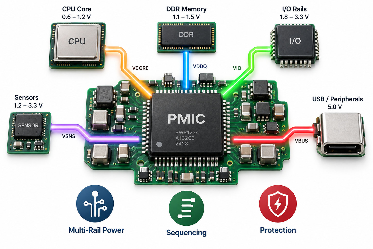
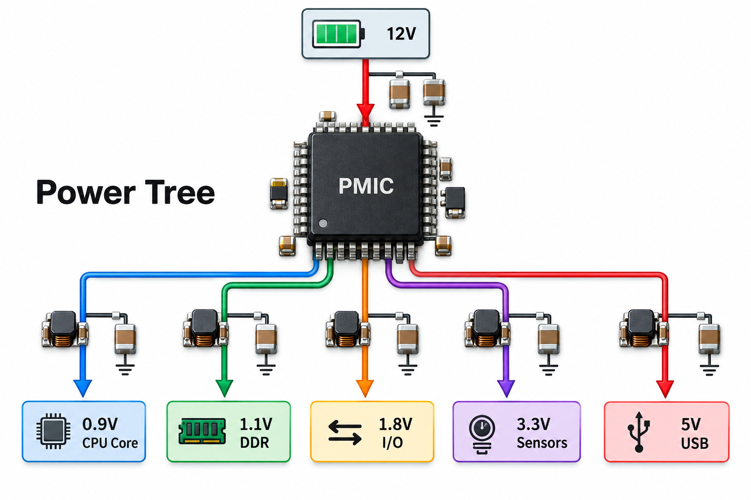
A simple product may need only one regulated voltage, but a modern processor-based PCB can require several rails such as:
- 0.8–1.0 V processor core
- 1.1 V memory
- 1.8 V I/O
- 3.3 V peripherals
- 5 V USB or auxiliary circuits
Instead of using one independent regulator for every rail, a PMIC can combine several power converters and control functions in one package.
The term PMIC can also be used broadly by semiconductor distributors for many power-management IC categories. In practical embedded design, however, “a PMIC” usually refers to a more integrated device that manages several power domains or system-level power functions.
What Functions Can a PMIC Integrate?
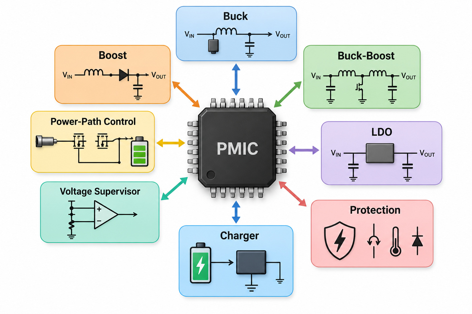
A PMIC can combine several power-conversion and control blocks that would otherwise require multiple ICs and supporting components.
| PMIC Function | What It Does |
|---|---|
| Buck converter | Steps voltage down efficiently |
| Boost converter | Steps voltage up |
| Buck-boost converter | Regulates when input may be above or below output |
| LDO | Provides low-noise regulated voltage |
| Sequencer | Controls rail startup and shutdown order |
| Battery charger | Manages charging current and voltage |
| Power-path controller | Selects or manages available power sources |
| Voltage supervisor | Monitors rails and generates reset/fault signals |
| Load switch | Connects or disconnects downstream loads |
| Protection circuit | Handles overcurrent, overvoltage, undervoltage, or thermal faults |
Not every PMIC includes all of these functions. A processor-oriented PMIC may focus on several buck converters, LDOs, sequencing, and monitoring, while a battery-powered device may place more emphasis on charging, power-path control, and low quiescent current.
This integration reduces the number of separate control ICs, but external inductors, capacitors, resistors, and sometimes MOSFETs may still be required.
How Does a PMIC Work in a Multi-Rail Power Tree?
A PMIC sits between the main power source and the different voltage domains required by the system.
A simplified power tree might look like:
12 V / 5 V / Battery Input → PMIC → 0.9 V CPU core / 1.1 V DDR memory / 1.8 V I/O / 3.3 V sensors and peripherals / 5 V USB or auxiliary load
Each rail can have different voltage, current, noise, and startup requirements. The PMIC coordinates these rails instead of treating them as independent power supplies.
A switching converter is normally used where efficiency matters, while an LDO may supply a lower-current rail that needs less noise. Some designs also allow rails to be reprogrammed through I²C, SPI, or stored configuration.
For processor and FPGA projects, EBest Circuit can review the power tree together with PMIC placement, external power components, current paths, and PCB stackup during DFM before fabrication.
How Does PMIC Power Sequencing Work?
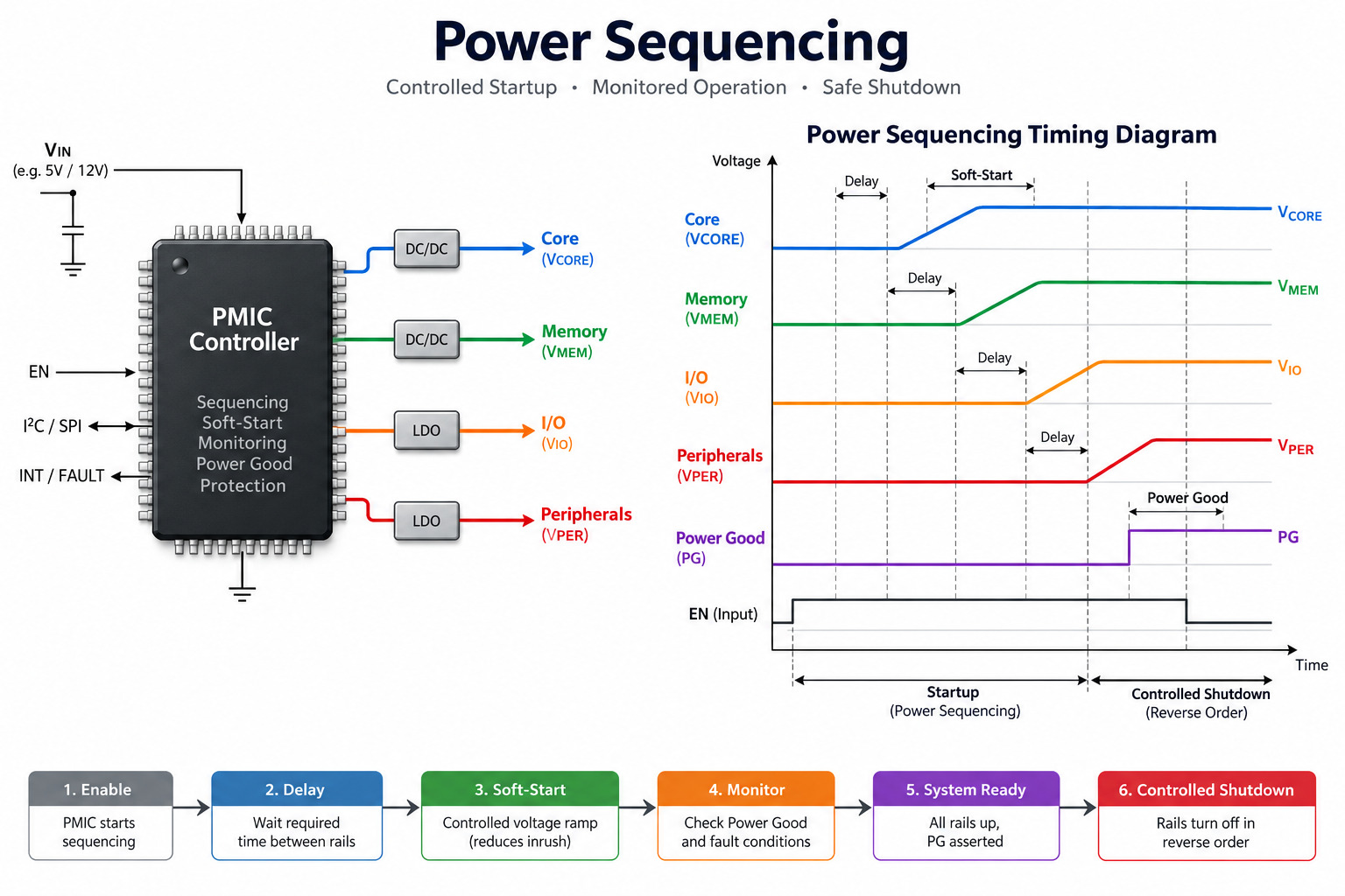
Power sequencing controls the order and timing in which voltage rails turn on and off.
Processors, FPGAs, DDR memory, and other complex ICs may require one rail to stabilize before another starts. Applying the wrong voltage first can cause excessive current, startup failure, latch-up, or undefined device behavior.
A simplified startup sequence might be:
Core rail → Memory rail → I/O rail → Peripheral rail
A PMIC may control this using:
- Programmable delay times
- Soft-start ramps
- Power-good signals
- Enable outputs
- Voltage monitoring
- Reset generation
- Fault shutdown
- Controlled reverse sequencing during power-down
Some PMICs use fixed factory sequencing, while others allow the sequence to be programmed through registers or nonvolatile configuration.
Power-down behavior matters as much as startup. Certain processors require rails to fall in a defined order so that I/O pins, memory, or analog sections are not left biased incorrectly during shutdown.
PMIC vs Voltage Regulator vs DC-DC Converter: What Is the Difference?
A voltage regulator or DC-DC converter normally focuses on one power-conversion function, while a PMIC can coordinate several power rails and supervisory functions.
| Feature | PMIC | Voltage Regulator | DC-DC Converter |
|---|---|---|---|
| Typical rail count | Multiple | Usually one | Usually one |
| Voltage regulation | Yes | Yes | Yes |
| Buck/boost conversion | Often several | Device dependent | Main function |
| Sequencing | Often | Usually limited | Usually limited |
| Monitoring | Often integrated | Basic or limited | Basic or limited |
| Battery management | Possible | Rare | Rare |
| Digital programming | Often available | Less common | Device dependent |
| System-level control | Strong | Limited | Limited |
An LDO is a voltage regulator. A buck converter is a DC-DC regulator. Both may be part of a PMIC.
The distinction is therefore mainly about integration and system coordination, not whether the IC can regulate voltage.
A design with one 3.3 V rail may not need a PMIC at all. A processor board with six rails, sequencing, reset logic, fault monitoring, and low-power modes is a much stronger PMIC application.
PMIC vs Discrete Power Design: When Does Integration Make Sense?
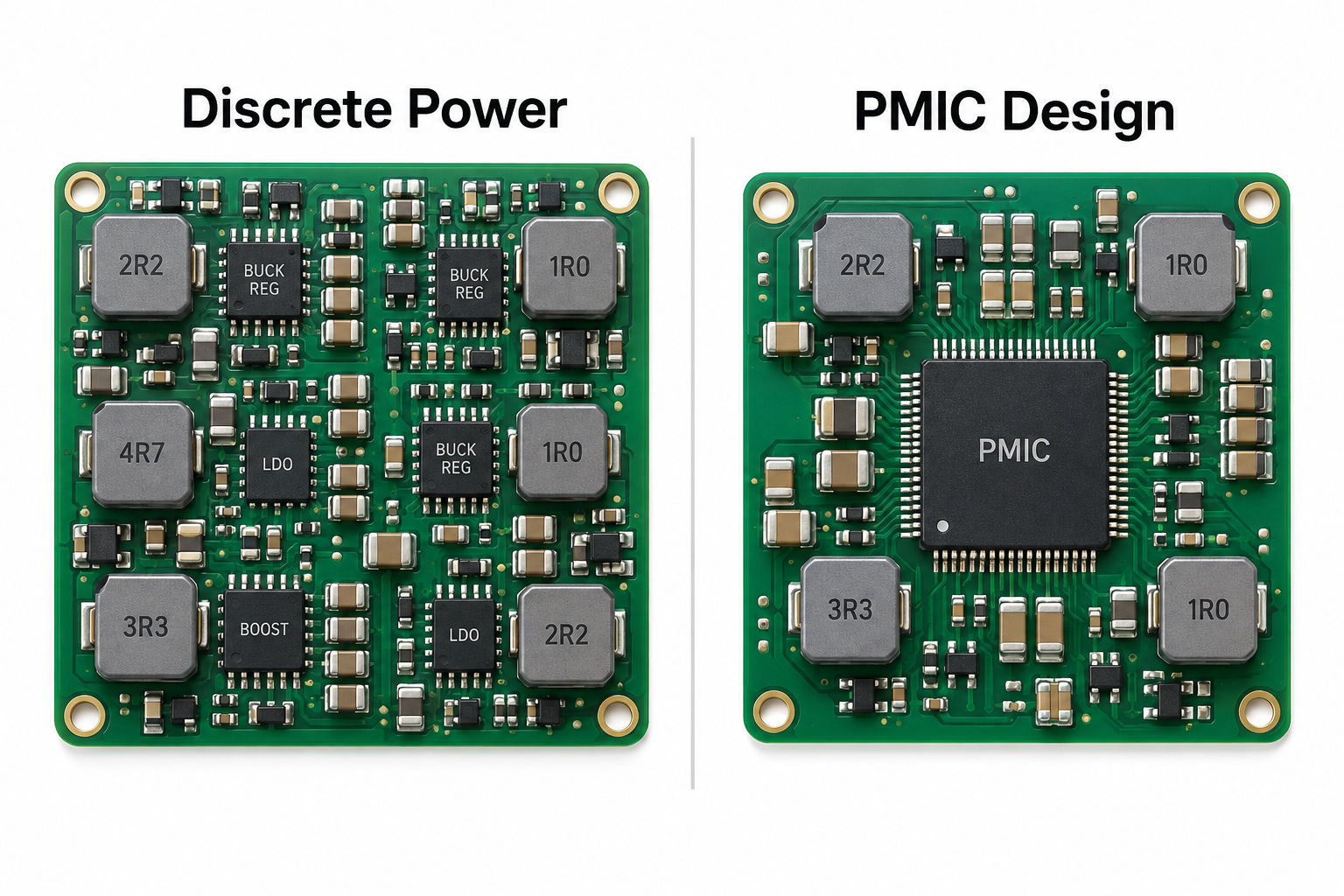
A PMIC becomes more attractive as the number of power rails and coordination requirements increase.
PMIC advantages include:
- Smaller PCB area
- Fewer separate control ICs
- Integrated sequencing
- Central fault monitoring
- Programmable rail control
- Reduced system-level design complexity
- Coordinated low-power modes
A discrete design can still be the better choice when:
- Only one or two rails are needed
- Rail requirements change frequently
- Different regulator vendors must be second-sourced
- Heat needs to be distributed across the PCB
- One rail requires an unusual converter topology
- Independent replacement or qualification matters
A PMIC can also create sourcing concentration because several rails depend on one component. If that device becomes unavailable, replacing it may require more redesign than replacing one discrete regulator.
The decision should therefore consider not only board area and BOM count, but also lifecycle, sourcing, thermal distribution, and firmware configuration.
Key Specifications When Selecting a PMIC
Selecting a PMIC starts with the complete power tree, not simply the number of output channels. Input conditions, rail voltage, peak current, transient response, efficiency, sequencing, thermal limits, and control interfaces should all be checked against the processor and system requirements.
The ranges can vary significantly between PMIC families. For example, TI’s TPS65219-Q1 accepts up to 5.5 V, integrates 3 buck converters and 4 LDOs, provides up to 3.5 A from its highest-current buck, and switches at up to about 2.3 MHz. ST’s STPMIC1L also accepts 2.8–5.5 V, provides two buck converters rated up to 2 A, and operates at 2 MHz.
| Specification | Check Item | Typical PMIC Specifications |
|---|---|---|
| Input voltage range | Normal input, tolerance, startup and transient conditions | STPMIC1L: 2.8–5.5 V; TPS65219-Q1: up to 5.5 V |
| Output rail count | Number of buck, boost and LDO rails required | TPS65219-Q1: 3 buck + 4 LDO |
| Output voltage range | CPU core, DDR, I/O and peripheral voltages | TPS65219-Q1: 0.6–3.4 V; STPMIC1L BUCK1: 0.5–4.2 V depending on mode |
| Output current | Continuous, peak and startup current on each rail | TPS65219-Q1: 3.5 A + 2 A + 2 A buck capability |
| Voltage accuracy | Processor/DDR rail tolerance over line, load and temperature | STPMIC1L buck regulation: typically around the ±1% to ±1.5% class, depending on rail and condition |
| Efficiency | Efficiency at real operating loads, not only peak value | Modern buck stages commonly operate in the 80–90%+ range, depending on VIN, VOUT and load |
| Quiescent current | Standby power and battery-life impact | TPS65219-Q1: about 250 µA typical |
| Switching frequency | Inductor size, ripple, EMI and switching loss | STPMIC1L: 2 MHz; TPS65219-Q1: up to about 2.3 MHz |
| Sequencing | Power-up/down order, delay, ramp and power-good behavior | Programmable sequencing is available on many processor PMICs |
| Protection | OCP, OVP, UVLO, thermal shutdown and fault reporting | Feature set varies by PMIC |
| Digital control | I²C, SPI or other runtime configuration | TPS65219-Q1 and STPMIC1L support I²C |
| Package / thermal path | PCB area, exposed pad and heat transfer | STPMIC1L: 4 × 4 × 1 mm VFQFPN-28 |
Protection features should also match the application. Useful functions can include:
- Overcurrent protection (OCP)
- Overvoltage protection (OVP)
- Undervoltage lockout (UVLO)
- Thermal shutdown
- Short-circuit protection
- Soft start
- Output discharge
- Power-good and fault reporting
Finally, do not select a PMIC from electrical specifications alone. Package size, exposed thermal pad, junction temperature, PCB copper area, thermal vias, external inductors and capacitors all affect how much usable power the PMIC can deliver in the finished board.
Where Are PMICs Used?
PMICs are common wherever electronic systems require several controlled voltage domains in limited PCB space.
Typical applications include:
- Smartphones
- Tablets
- Wearables
- IoT devices
- Edge AI hardware
- Embedded Linux systems
- FPGA boards
- Automotive infotainment
- ADAS electronics
- Industrial control systems
- Medical devices
- Networking equipment
- Cameras and imaging systems
A smartphone PMIC may manage the processor, memory, display, camera, radio, battery, and always-on rails.
An FPGA or edge-computing board may use a PMIC to supply core, auxiliary, I/O, memory, and transceiver voltages in a defined sequence.
Automotive PMICs may add watchdogs, safety monitoring, protected outputs, and communication with the main processor. The underlying architecture changes by application, but the common requirement is coordinated management of several power domains.
What PCB Layout Rules Matter for a PMIC?
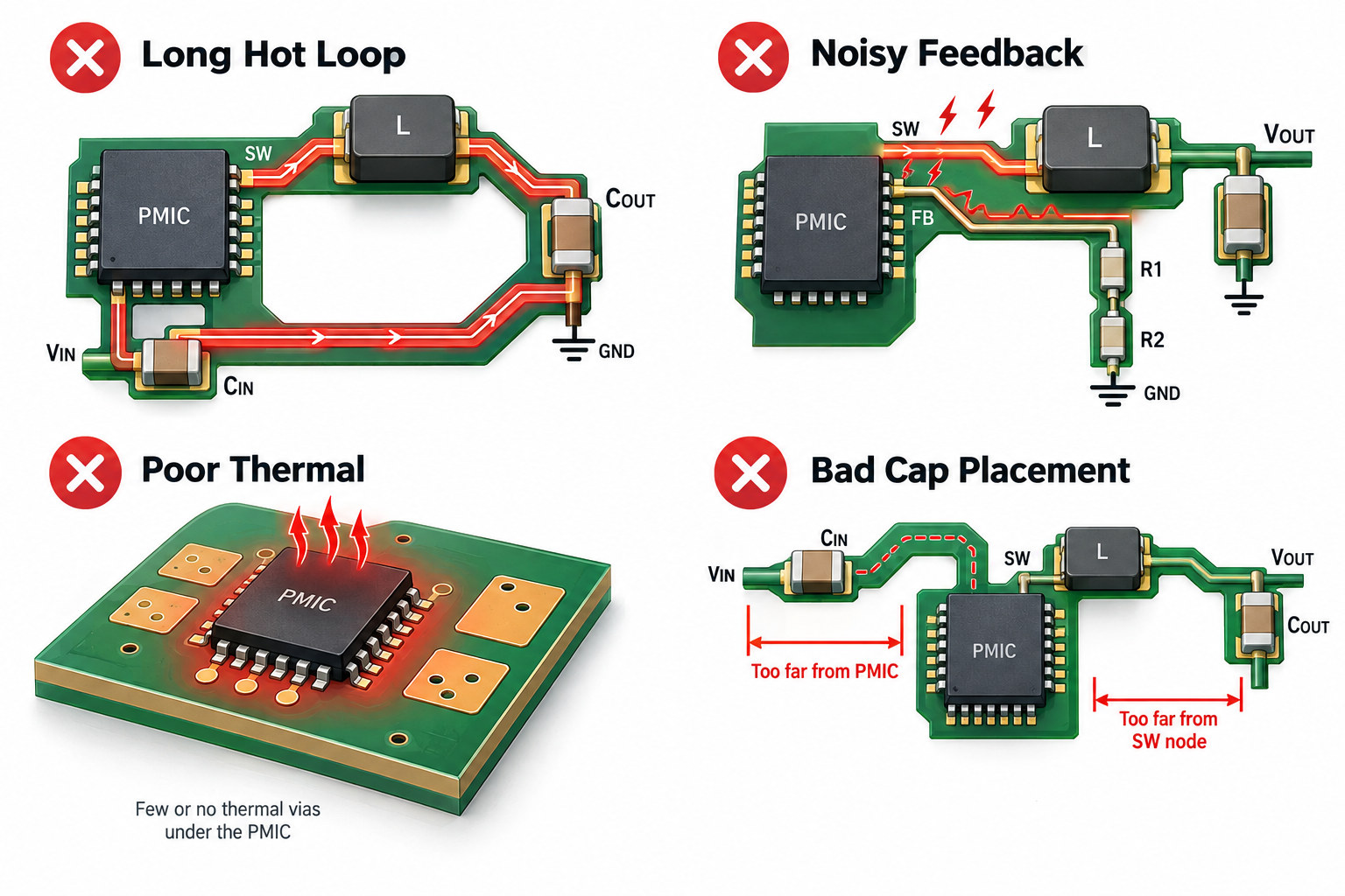
PMIC PCB layout is critical because switching converters combine high current, fast switching edges, sensitive feedback nodes, and thermal dissipation within a small area.
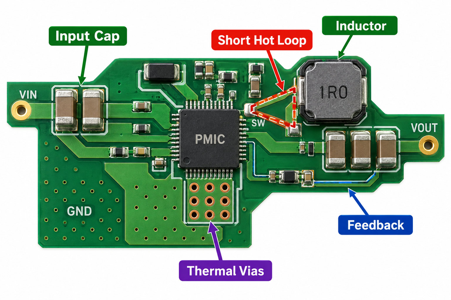
Important layout rules include:
- Place input capacitors close to VIN and power ground.
- Minimize high-di/dt switching loops.
- Keep inductors close to switching pins.
- Keep the SW node compact.
- Route feedback away from noisy switching nodes.
- Use wide copper for high-current paths.
- Provide low-impedance ground return paths.
- Place output capacitors close to their rails.
- Use thermal vias under exposed pads where required.
- Avoid routing sensitive analog signals through switching-current paths.
The input capacitor, switching FETs, inductor, and output capacitor form critical current loops. Increasing their loop area raises parasitic inductance and can worsen ringing, EMI, and voltage ripple.
Grounding also needs to follow the PMIC vendor’s recommended layout. Analog ground, power ground, thermal pad connections, and feedback return paths should not be rearranged casually because the schematic appears electrically equivalent.
EBest Circuit can review PMIC placement, high-current copper, thermal vias, power planes, component spacing, and assembly requirements during PCB DFM.
What Common PMIC Design Mistakes Cause Power Problems?
PMIC problems often come from system integration rather than a defective IC.
Common mistakes include:
- Selecting a rail with insufficient output current
- Ignoring processor startup or transient current
- Using the wrong startup sequence
- Incorrect power-down timing
- Poor input or output capacitor placement
- Choosing the wrong inductor
- Routing feedback close to the SW node
- Making switching hot loops too large
- Inadequate thermal vias
- Excessive copper loss on high-current rails
- Ignoring PMIC configuration or OTP settings
- Using the wrong I²C address
- Forgetting power-good or reset timing requirements
- Assuming every rail can run at maximum current simultaneously
Thermal design is another frequent issue. A PMIC supplying several rails can dissipate significant heat even when individual converters operate efficiently.
The exposed thermal pad, PCB copper area, via array, airflow, ambient temperature, and neighboring heat sources all affect junction temperature.
Startup testing should therefore be performed with the real processor, memory, and peripherals rather than only checking the PMIC outputs with no load.
How Should a PMIC Design Be Prepared for PCB Assembly and Testing?
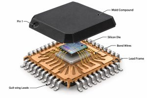
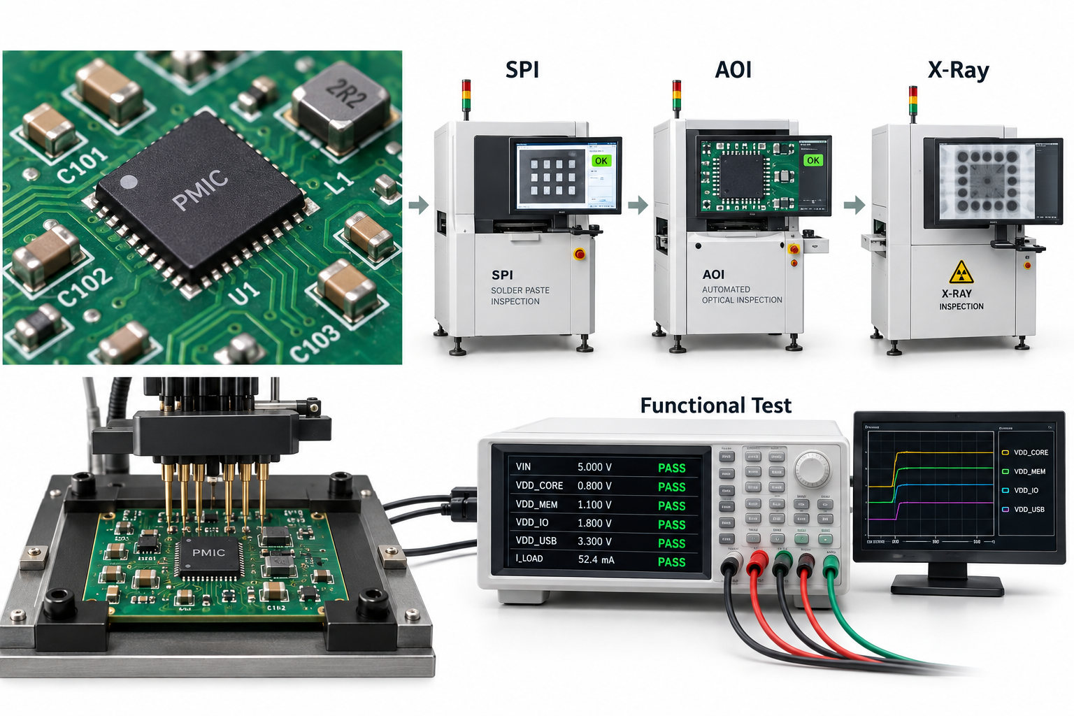
PMIC assembly requirements depend strongly on the package. QFN, BGA, and WLCSP devices need different stencil, placement, inspection, and rework strategies.
For QFN PMICs, review:
- Exposed thermal pad
- Paste aperture ratio
- Thermal via layout
- Solder-mask definition
- Void control
- Package orientation
For BGA or WLCSP packages, additional concerns include:
- Fine-pitch pad geometry
- Via-in-pad requirements
- Solder-mask registration
- Board warpage
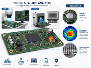
- X-ray inspection
- Rework capability
A production test plan should verify more than static output voltage. Useful checks can include:
- Rail startup sequence
- Rail shutdown sequence
- Output-voltage accuracy
- Ripple
- Load response
- Power-good timing
- Reset timing
- Fault response
- I²C/SPI communication
- Thermal behavior under load
SPI can verify solder-paste deposition before placement, while AOI helps inspect visible joints and nearby passives. X-ray is particularly useful for hidden BGA/WLCSP joints and exposed-pad voiding where relevant.
FAQ About PMIC Power Management ICs
1. What does PMIC stand for?
The PMIC full form is Power Management Integrated Circuit.
2. What is PMIC in electronics?
The PMIC meaning in electronics is a chip that generates, regulates, sequences, monitors, and protects one or more system power rails.
3. Is a PMIC chip the same as a voltage regulator?
No. A voltage regulator normally controls one rail, while a PMIC chip can integrate several regulators plus sequencing, monitoring, protection, charging, or digital control.
4. Does a PMIC need external components?
Usually yes. Depending on the architecture, a PMIC may require external inductors, input and output capacitors, resistors, sense components, and sometimes external MOSFETs.
5. Why is power sequencing important in a PMIC?
Processors, memory, and I/O rails may need to start and stop in a defined order. Incorrect sequencing can cause startup failure, excessive current, or undefined system behavior.
6. Can one PMIC power a processor, memory and peripherals?
Yes, if the PMIC provides the required number of rails, voltage ranges, output currents, sequencing, and total thermal capacity.
Planning a PCB Around a PMIC?
A PMIC can simplify a complex power tree, but its performance still depends on the surrounding PCB. High-current loops, inductors, decoupling, feedback routing, thermal pads, sequencing signals, and assembly quality all need to be considered together.
EBest Circuit supports PMIC-based PCB fabrication, DFM review, fine-pitch SMT assembly, component sourcing, SPI, AOI, X-ray inspection, and functional testing. For a new power-management PCB project, send your Gerber files, BOM, schematic, stackup, and power requirements to sales@bestpcbs.com for engineering review.