modular PCB design divides an electronic system into defined functional boards or circuit blocks that can be developed, verified, replaced, and reused with controlled interfaces. It is useful when a product family needs several configurations, when different teams work in parallel, or when one subsystem is likely to change before the rest of the product.
The method does not make a system reliable by itself. A module boundary adds connectors, return-path transitions, power-entry conditions, mechanical tolerances, and version-control decisions. The design succeeds only when those interfaces are treated as engineering specifications rather than convenient pin headers added near the end of layout.
What Is Modular PCB Design?
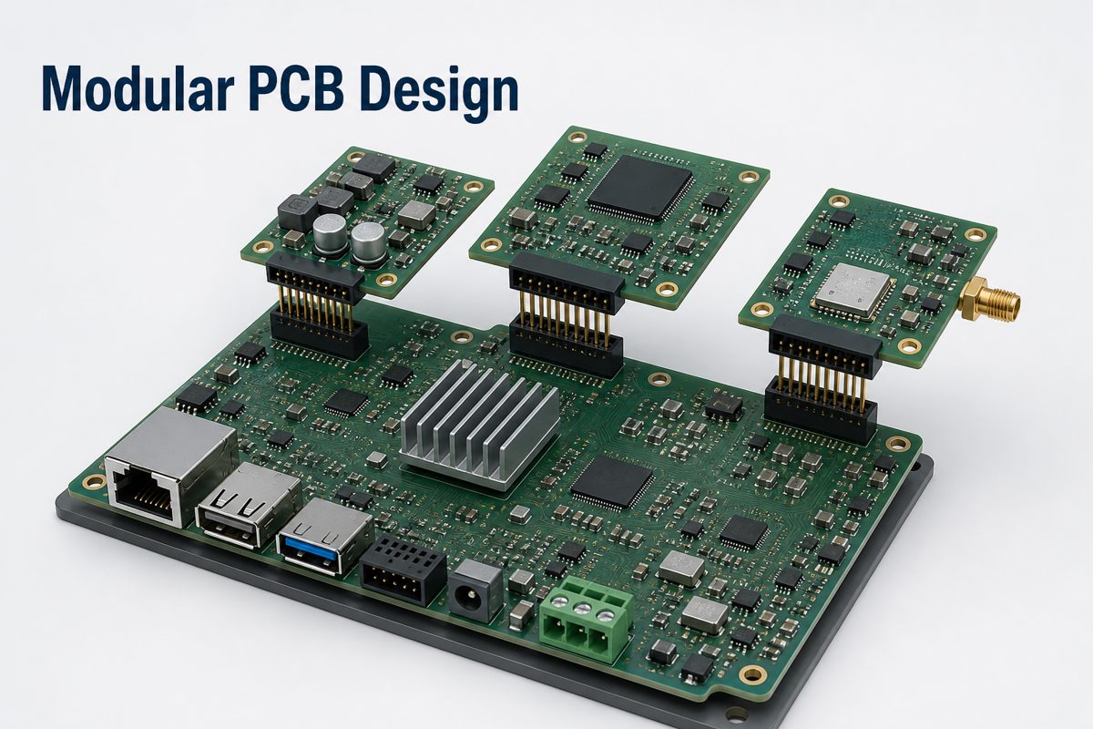
Modular PCB design is a system architecture in which each module has a defined function, a controlled interface, and a clear verification boundary. A module might handle power conversion, processing, sensing, motor control, communication, data acquisition, or a user interface.
Modularity can exist at two levels:
- Logical modularity: functional blocks remain on one PCB but use separate schematic sheets, layout zones, power domains, and test boundaries.
- Physical modularity: functions are placed on separate boards connected by mezzanine connectors, card-edge contacts, cables, backplanes, or soldered modules.
A product does not need multiple boards to benefit from modular thinking. Even a single-board design becomes easier to review when power, analog, digital, RF, and safety-related sections have explicit boundaries. Physical separation is justified when it improves reuse, serviceability, configuration control, parallel development, enclosure fit, or risk isolation enough to offset the added interconnect cost.
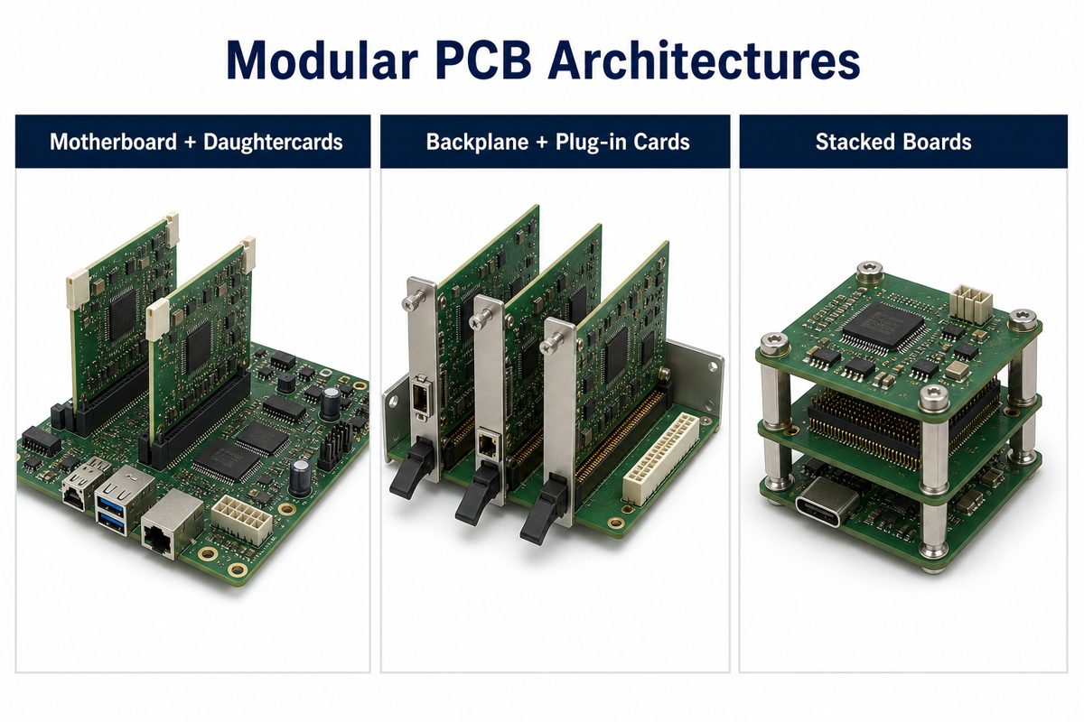
Which Modular PCB Architecture Fits the System?
The best architecture follows the product’s service model, signal bandwidth, available volume, mechanical envelope, and expected upgrade path. It should not be chosen only because stacked boards look compact.
| Architecture | Best Fit | Main Constraint |
| Motherboard with daughtercards | Products with optional or replaceable functions | Connector alignment, stack height, and local support |
| Backplane with plug-in cards | Expandable industrial, communications, and test systems | Shared power, bus loading, card guides, and airflow |
| Stacked boards | Compact embedded devices with limited footprint | Thermal shadowing, inspection access, and tolerance stack |
| Cable-linked boards | Modules placed around an enclosure or moving assembly | Cable loss, EMI, strain relief, and connector retention |
| Soldered castellated module | Reusable RF, sensing, or processing subassemblies | Reflow profile, pad geometry, rework, and test access |
For a deeper look at stacked structures and their assembly implications, compare this architecture decision with our PCB on PCB design guide. That physical stacking decision is only one part of a complete modular system.
How Should Functional Boundaries Be Defined?
Start with functions and failure domains, not arbitrary board outlines. A useful boundary minimizes the number of signals crossing between modules while keeping each module independently understandable and testable.
Review each proposed boundary against these questions:
- Does the module perform one coherent function with clear inputs and outputs?
- Can it be powered, programmed, and tested without the complete product?
- Are high-current paths, precision analog signals, clocks, RF feeds, or safety barriers being forced through an unnecessary connector?
- Will the module be reused across enough products or variants to justify interface control and separate lifecycle management?
- Can a failed module be isolated without replacing a large portion of the system?
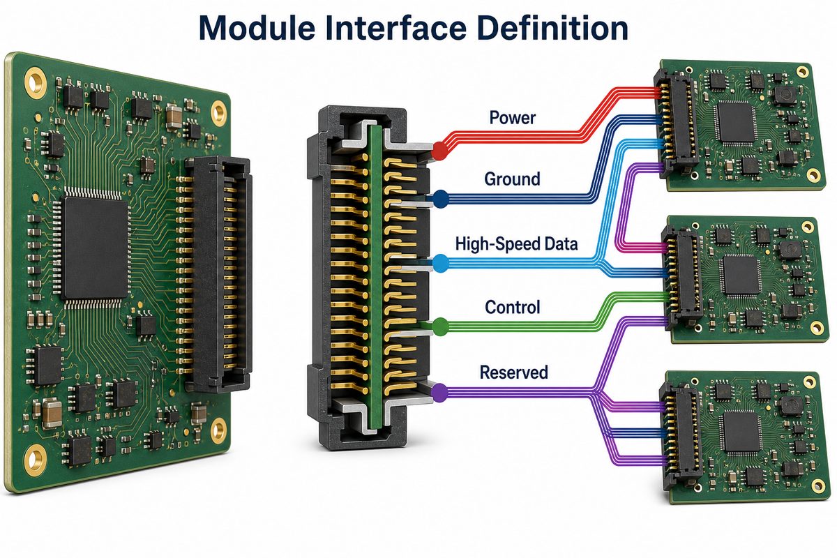
Create an interface control document before detailed layout. It should identify every pin, direction, electrical level, power state, allowable load, timing requirement, reference ground, pull-up ownership, default state, reserved position, mating sequence, and compatibility rule. The document should also state which module revision is compatible with each host-board revision.
How Should a Modular PCB Connector Be Specified?
A modular PCB connector must be selected as an electrical, mechanical, assembly, and service component at the same time. Pitch and pin count alone are not enough.
- Electrical: current per contact, contact resistance, voltage rating, ground-to-signal ratio, shielding, and high-speed performance.
- Mechanical: mating height, insertion force, retention, alignment features, durability cycles, keying, and tolerance to vibration or shock.
- Assembly: SMT or through-hole termination, coplanarity, reflow compatibility, paste design, inspection access, and repair method.
- Lifecycle: availability, second-source strategy, connector revision control, and the consequence of obsolescence.
Place ground contacts beside sensitive or fast signals when the connector system supports it. Avoid assigning every ground pin to one end of a long connector because that can force return current to take a larger loop. For removable modules, add polarization or mechanical keying so an incompatible card cannot be inserted in the wrong orientation.
How Do Signal Integrity and Return Paths Cross Module Boundaries?
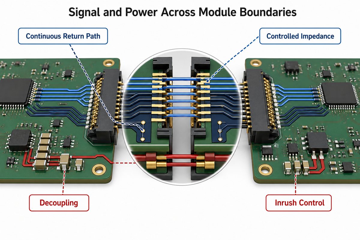
Every connector is an impedance discontinuity. The signal sees PCB traces, pads, vias, contacts, another set of pads and vias, then a second PCB. At low edge rates this transition may be forgiving; at high edge rates it can create reflection, loss, crosstalk, mode conversion, and timing error.
Control the complete channel rather than checking each board in isolation:
- Route fast signals over continuous reference planes up to the connector launch.
- Provide nearby ground contacts so return current can cross the same physical boundary.
- Minimize stubs, unused connector branches, and unnecessary layer changes.
- Keep differential pair geometry and skew controlled through both launches.
- Include connector models, via models, and both PCB stackups in channel simulation when the data rate requires it.
- Define whether termination is located on the source module, destination module, or backplane.
Our high-speed digital PCB guide explains controlled impedance, differential pairs, vias, crosstalk, and return-path planning in more detail.
How Should Power Be Distributed Across Modular Circuit Boards?
Power architecture should be defined before connector pinout. Decide whether the host distributes raw input power, regulated system rails, or both. A raw-bus approach gives each module local regulation and fault isolation, while shared regulated rails can reduce duplicate circuitry but make voltage drop, transient loading, and compatibility more sensitive.
For every rail crossing modular circuit boards, document:
- Nominal voltage, tolerance, continuous current, peak current, and startup current.
- Contact allocation, current derating, acceptable voltage drop, and temperature rise.
- Power-up and power-down sequence, reset behavior, and back-powering risks through signal pins.
- Local input capacitance, decoupling, bulk storage, and load-transient limits.
- Fuse, current-limit, reverse-polarity, overvoltage, and fault-containment strategy.
- Whether live insertion is prohibited or intentionally supported.
Do not assume a removable card is hot-swappable. Live insertion may require staggered contacts, pre-charge, inrush control, power-good logic, and firmware behavior that prevents undefined bus activity. If the product is serviced only when powered off, say so clearly in the interface and service documentation.
Which Mechanical and Thermal Constraints Need Early Control?
A modular electrical design can fail at integration because the boards do not mate reliably, the enclosure loads the connector, or one card blocks airflow to another. Use the mechanical model early enough to influence board outline and placement.
- Set connector location, mating height, board spacing, and allowable positional tolerance as shared dimensions.
- Add guide pins, card guides, standoffs, screws, latches, or enclosure features when the connector should not carry the full mechanical load.
- Check keep-outs around extraction paths, fasteners, cable bends, test probes, and rework tools.
- Model component height on both sides of every board, including manufacturing tolerances.
- Review heat-source alignment, airflow blockage, heatsink access, and thermal coupling between stacked modules.
- Define the expected insertion cycles and service environment before choosing a connector family.
Mechanical reference points must match across the PCB outline, assembly drawing, enclosure model, and connector drawing. Small coordinate or revision errors can create a system-level interference even when each individual board passes inspection.
How Should Each Modular PCB Board Be Prepared for Manufacturing?
Each modular PCB board needs its own buildable data package plus one system-level document that connects the revisions. Reusing a circuit block does not mean reusing an old manufacturing package without checking its current components, stackup, footprint data, and interface revision.
Before release, apply the same fabrication and assembly discipline to every module:
- Gerber or approved intelligent data, NC drill files, board outline, and fabrication drawing.
- Stackup, controlled-impedance requirements, material, copper, finish, thickness, and tolerances.
- BOM, centroid data, assembly drawing, polarity notes, approved substitutions, and do-not-fit variants.
- Connector part numbers, mating orientation, stack height, keep-outs, and inspection requirements.
- Programming files, module serial or revision marking, test procedure, and pass/fail limits.
Run a PCB design for manufacturability review on each board and then repeat the review at the system level. The second pass catches problems that a board-only check misses, such as inaccessible connectors, blocked test points, conflicting revisions, and assembly-order constraints.
How Should a Modular PCB System Be Tested?
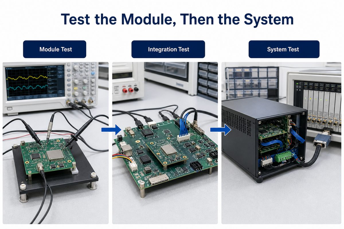
A modular PCB system should be verified in layers: module test, interface integration test, and complete system test. Passing a module-level functional test does not prove that the connector channel, shared power network, firmware handshake, enclosure, or thermal environment will work after integration.
- Test each module independently. Verify its power input, outputs, communications, programming, protection, and boundary conditions.
- Use known-good counterparts. A golden host board or golden module helps isolate whether a failure follows the module or the interface.
- Test every interface state. Include startup, reset, sleep, communication loss, overload, missing module, incorrect revision, and permitted insertion or removal conditions.
- Validate the complete assembly. Measure signal margins, rail behavior, temperatures, EMI-sensitive conditions, and performance inside the final enclosure.
- Preserve traceability. Record board revision, firmware version, BOM variant, module serial number, and test result as one system configuration.
Test points should remain accessible before and after modules are installed. If a fixture cannot contact critical nets in the assembled state, provide a dedicated test connector, boundary-scan path, built-in self-test, or another agreed diagnostic interface.
When Does a Modular Design Add Cost or Risk?
Modularity is not automatically cheaper. It can reduce redesign and service cost while increasing unit hardware cost. The correct comparison uses total product and lifecycle impact, not the PCB price alone.
| Potential Benefit | Possible Added Cost or Risk |
| Reuse of validated functions | Interface documentation and compatibility validation |
| Parallel development | More coordination, revision control, and integration testing |
| Replaceable or upgradeable modules | Connectors, retention hardware, enclosure volume, and service access |
| Fault isolation | Extra protection, diagnostic circuitry, and test fixtures |
| Product configuration from common blocks | Variant management, inventory, and end-of-life coordination |
A monolithic board may be better when the product is small, cost-sensitive, built in one stable configuration, and dominated by short high-speed or high-current paths. A modular architecture becomes stronger when the product family changes frequently, field replacement matters, teams can truly work in parallel, or validated functions will be reused across several products.
FAQ About Modular PCB Design
- Is a modular PCB the same as a daughterboard? No. A daughterboard is one physical module type. Modular design also includes backplanes, stacked boards, cable-linked assemblies, soldered modules, and logical blocks on one PCB.
- Can a modular PCB improve repairability? Yes, when failed functions can be diagnosed and replaced independently. Repairability still depends on accessible connectors, spare-module control, service documentation, and safe replacement procedures.
- Are board-to-board connectors suitable for high-speed signals? They can be, but the connector, launches, vias, reference contacts, stackups, and complete channel must meet the interface bandwidth and signal-integrity requirements.
- Should every module use the same connector? Not necessarily. Standardization helps reuse, but power, high-speed, RF, safety, mechanical, and environmental requirements may justify different connector families.
- What files are needed to quote a multi-board assembly? Provide the fabrication package for every PCB, BOM and placement data for every assembly, mechanical drawings, the module/interface definition, test requirements, quantities, variants, and one revision matrix for the full system.
The most important rule is to treat modular PCB design as a controlled system architecture. Reusable boards are valuable only when their electrical, mechanical, firmware, manufacturing, and test interfaces remain explicit.
How Can EBest Circuit Support Your Modular PCB Project?
At EBest Circuit, we support PCB fabrication, component sourcing, PCBA assembly, DFM review, and agreed inspection or functional testing for multi-board electronic products. We can review the individual module files together with connector orientation, stack height, controlled-impedance needs, assembly sequence, and system test access before the build is released.
For a useful engineering review and quotation, send the Gerber or ODB++ data for each board, NC drill files, stackups, fabrication drawings, BOMs, placement files, assembly drawings, connector specifications, quantities, revision matrix, and test requirements. Our PCB manufacturing and assembly guide can help you organize that package.
Email sales@bestpcbs.com with your project files and system constraints. We will review the manufacturing and assembly scope against the actual module architecture instead of treating each PCB as an unrelated order.