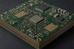
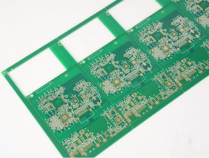
A mixed signal PCB integrates analog and digital circuits on a single board, making manufacturing accuracy critical to signal integrity, noise control, and overall circuit reliability. Proper material selection, stackup construction, impedance control, and grounding all contribute to consistent electrical performance. This guide explores mixed signal PCB manufacturing, fabrication requirements, assembly processes, testing methods, and cost considerations to help engineers and purchasing teams make informed manufacturing decisions.
At EBest Circuit (Best Technology), we provide integrated mixed signal PCB fabrication and assembly services, covering multilayer PCB production, component sourcing, SMT assembly, inspection, and functional testing. Our free DFM support, No MOQ policy, four SMT production lines, and MES single-board traceability help customers manage projects from prototype builds to repeat production. Whether you need a new manufacturing partner or want to streamline your existing supply chain, send your Gerber files, BOM, quantity, and project requirements to sales@bestpcbs.com for a technical review and quotation.
What Is a Mixed Signal PCB?
A mixed signal PCB is a printed circuit board that contains both analog and digital circuitry. It allows continuous electrical signals and digital processing functions to operate within one electronic system.
These boards commonly integrate analog-to-digital converters (ADCs), digital-to-analog converters (DACs), operational amplifiers, microcontrollers, sensors, and communication interfaces.
For manufacturers, the challenge is to fabricate a board that maintains the electrical characteristics established during circuit development.
Common mixed signal PCB applications include:
- Medical monitoring equipment: Sensor acquisition, analog filtering, and digital signal processing.
- Industrial control systems: Precision measurement, ADC conversion, and microcontroller-based control.
- Communication equipment: RF signal processing, frequency conversion, and digital interfaces.
- Automotive electronics: Sensor interfaces, data acquisition, and electronic control modules.
- Test and measurement instruments: Low-noise analog inputs, precision references, and digital analysis.
- IoT devices: Environmental sensing, wireless communication, and embedded processing.
A mixed signal board may require conventional multilayer FR4 fabrication or more advanced structures involving HDI technology, tighter impedance control, and specialized materials.
The appropriate construction depends on operating frequency, signal sensitivity, thermal conditions, and component density.
Mixed Signal PCB Design Guidelines for Manufacturing
Mixed signal PCB design guidelines should account for actual fabrication tolerances, material properties, and assembly constraints. A layout that performs well in simulation must also be practical to fabricate and reproduce.
For this reason, engineering review before production is particularly valuable.
Key manufacturing considerations include:
- Trace width and spacing: Confirm that critical analog and digital traces meet the manufacturer’s achievable geometry and tolerances.
- Layer alignment: Consider registration tolerances when placing narrow traces, buried features, and closely spaced vias.
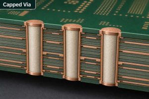
- Via structures: Select through-hole, blind, or buried vias according to routing density and production requirements.
- Copper distribution: Balance copper coverage where practical to support consistent lamination and plating.
- Component footprints: Check pad dimensions, solder-mask openings, and assembly clearance against the selected components.
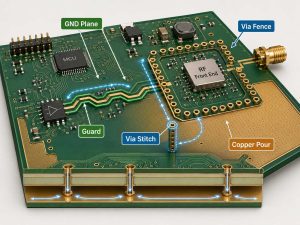
- Reference planes: Preserve continuous return-current paths for sensitive and high-speed signals.
Our DFM review focuses on the relationship between the released design and the selected manufacturing process. For example, an impedance-controlled trace may need an adjusted width after the actual laminate thickness and copper construction are confirmed.
Likewise, closely spaced ADC components, fine-pitch packages, and dense via fields may require additional review before the design is released for production.
Engineers can submit Gerber files, stackup details, drill files, and critical electrical requirements for evaluation. This helps identify practical manufacturing adjustments before boards enter production.
Mixed Signal PCB Layout and Partitioning for Production
Mixed signal PCB layout plays an important role in reducing interference between analog and digital circuits. However, effective partitioning does not simply mean separating the board into two isolated copper regions.
The main objective is to control where signals travel, how return currents flow, and how noisy circuitry interacts with sensitive analog sections.
Important layout considerations include:
- Analog and digital placement: Group related components by function, keeping low-level analog circuits away from high-current switching nodes.
- ADC and DAC placement: Position conversion devices close to their associated analog signal paths and supporting components.
- Clock routing: Keep fast clock traces away from sensitive analog inputs and voltage-reference connections.
- Power distribution: Provide suitable filtering and decoupling for analog and digital supply domains.
- Signal return paths: Maintain a continuous reference beneath critical traces wherever practical.
- Via transitions: Account for changes in reference planes when signals move between layers.
For example, an industrial data acquisition PCB may include an analog sensor interface, a precision ADC, and a microcontroller.
Placing the analog front end near its input connector can shorten sensitive signal paths. Locating the microcontroller and associated switching circuits in a separate functional region can reduce unwanted coupling.
From a fabrication perspective, the manufacturer must preserve the intended copper geometry, layer registration, and reference-plane structure.
A well-planned layout also improves manufacturing efficiency. Clear routing, suitable component clearance, and manufacturable via structures help reduce the need for design changes during production.
Mixed Signal PCB Stackup and Material Selection
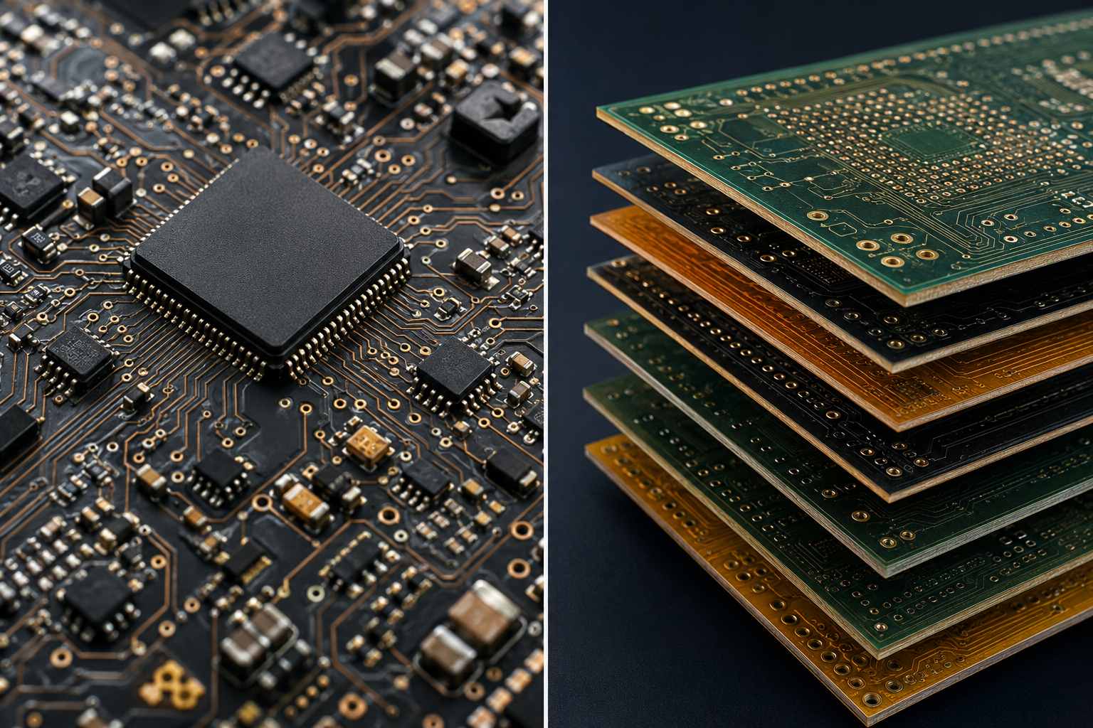
Mixed signal PCB stackup determines the arrangement of signal, ground, and power layers. It affects impedance, electromagnetic coupling, power distribution, and the routing space available for analog and digital circuits.
Four-layer and six-layer constructions are common starting points, while denser or more demanding applications may require eight or more layers.
The final structure should be selected according to circuit requirements rather than layer count alone.
Typical mixed signal PCB stackup options
| PCB Layers | Typical Construction | Suitable Applications |
|---|---|---|
| 4 Layers | Signal / GND / Power / Signal | Compact ADC and MCU boards |
| 6 Layers | Signal / GND / Signal / Signal / Power / Signal | Industrial control and data acquisition |
| 8 Layers | Multiple signal and reference planes | Dense, high-speed mixed signal systems |
These are illustrative configurations, not universal production stackups. A six-layer board, for example, may benefit from additional ground referencing or a different plane arrangement. The final construction must be reviewed against routing, EMC, and impedance requirements.
Material Selection
For many mixed signal applications, standard FR4 provides a practical balance between cost and electrical performance. Higher-frequency circuits or demanding thermal environments may require alternative materials.
| PCB Material | Main Characteristic | Typical Use |
|---|---|---|
| Standard FR4 | Cost-effective multilayer construction | General industrial electronics |
| High-Tg FR4 | Higher glass-transition temperature | Elevated thermal demands |
| Low-Loss Laminate | Reduced dielectric loss | High-frequency signal paths |
| Hybrid Laminate | Combines different material properties | Mixed RF and digital circuits |
Material selection should consider dielectric constant, dissipation factor, thermal expansion, operating temperature, and procurement availability.
Controlled Impedance Requirements
For impedance-sensitive traces, several manufacturing parameters must be evaluated together:
- Finished trace width and copper thickness
- Dielectric thickness and material properties
- Spacing between differential conductors
- Distance from traces to reference planes
- Fabrication tolerances and impedance verification
A nominal 50-ohm single-ended trace or 100-ohm differential pair is only a common design target. Actual impedance requirements depend on the interface and circuit design.
At EBest Circuit, engineers can provide the target impedance, preferred stackup, and applicable tolerances for a manufacturing review. The final trace geometry should be agreed upon before fabrication.
Mixed Signal PCB Fabrication and Impedance Control
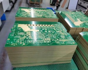
Mixed signal PCB fabrication requires consistent control of copper patterns, dielectric structures, plated holes, and surface finishes.
Unlike a simple board used for low-frequency switching, a mixed signal circuit may contain sensitive analog traces alongside fast digital connections and multiple power domains.
Manufacturing variation can affect these features differently.
Our PCB fabrication services support the following requirements:
| Manufacturing Feature | Available Solution |
|---|---|
| PCB Construction | Multilayer FR4, HDI, RF/microwave |
| Materials | Standard FR4, High-Tg, specialized laminates |
| Via Technology | Through-hole and HDI structures |
| Impedance | Controlled-impedance fabrication |
| Surface Finish | Project-specific finish selection |
| Quality Inspection | Optical, dimensional, and electrical inspection |
| Production Support | Prototypes and repeat manufacturing |
Specific line widths, spacing, drill sizes, layer counts, and impedance tolerances are confirmed against the board construction and fabrication drawings.
The most important manufacturing controls are:
1. Copper Geometry
Trace width, spacing, and finished copper thickness influence impedance and electrical resistance.
Controlled etching and appropriate process compensation help maintain the required conductor dimensions.
2. Lamination Consistency
Dielectric thickness affects the impedance of microstrip and stripline structures. Material selection and lamination conditions therefore need to match the approved stackup.
3. Drilling and Plating
Reliable plated through-holes and vias provide electrical connections between PCB layers. Hole geometry, plating quality, and interconnection reliability are particularly important in multilayer assemblies.
4. Impedance Verification
When specified, controlled-impedance production can include suitable test coupons and measurements against the agreed target and tolerance.
5. Electrical Inspection
Electrical testing helps identify opens and shorts before assembly. Additional structural inspections can be applied according to board complexity and customer specifications.
By coordinating stackup approval, fabrication, and assembly preparation, EBest Circuit helps customers establish a consistent build package for subsequent production orders.
PCB Grounding in Mixed Signal Design and Return Paths
PCB grounding in mixed signal design affects noise performance, signal integrity, and electromagnetic compatibility.
The main manufacturing concern is preserving the intended ground structure and avoiding unintended interruptions in signal return paths.
A continuous reference plane is often preferable for mixed signal boards because high-frequency return currents tend to flow close to their associated signal traces.
Separating analog and digital components into functional regions can reduce interference without requiring a physical split in the ground plane.
Grounding and return-path considerations
| PCB Feature | Recommended Approach |
|---|---|
| Ground Plane | Maintain continuous reference copper where practical |
| Analog Signals | Keep sensitive return paths localized |
| Digital Signals | Avoid routing across reference-plane gaps |
| ADC/DAC Grounding | Follow the device manufacturer’s guidance |
| Layer Transitions | Provide suitable reference continuity |
| Power Decoupling | Minimize connection inductance |
One common concern is whether analog ground (AGND) and digital ground (DGND) should be separated.
There is no universal answer for every device. Many mixed signal designs benefit from a shared, low-impedance ground plane combined with careful component partitioning. Other systems may require a specified connection between separate ground regions.
The ADC, DAC, or mixed signal IC manufacturer’s grounding recommendations should guide the final implementation.
An unnecessary ground-plane split can force a high-frequency return current to travel around a gap, increasing loop area and potentially introducing noise.
During fabrication, the approved ground geometry must be preserved. Changes to copper clearances, plane openings, or via arrangements should be reviewed whenever they affect critical return paths.
For boards with sensitive analog measurements, grounding requirements should be included in the engineering review rather than treated as ordinary copper-fill details.
Mixed Signal PCB Assembly and Testing Services
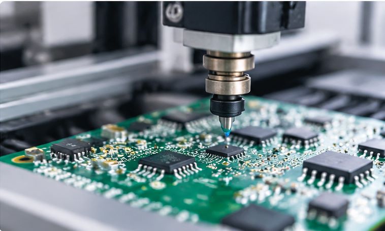
Mixed signal PCB assembly requires precise component placement, controlled soldering, and appropriate inspection methods.
Many assemblies combine small passive components, fine-pitch ICs, ADCs, DACs, microcontrollers, and connectors on a compact PCB.
The assembly process must support both electrical reliability and the performance of sensitive circuit functions.
At EBest Circuit, our PCB assembly services are supported by four SMT production lines, including two JUKI lines and two YAMAHA lines.
Our SMT and PCBA capabilities include:
| Assembly Capability | EBest Circuit |
|---|---|
| SMT Production | 4 lines |
| SMT Equipment | 2 JUKI + 2 YAMAHA |
| Smallest Components | 01005 |
| Fine-Pitch BGA | Down to 0.2 mm pitch |
| Soldering | Nitrogen reflow, wave, selective wave |
| Inspection | SPI, AOI, X-Ray |
| Electrical Testing | ICT and FCT |
| Additional Services | Programming, coating, box build |
| Traceability | MES single-board tracking |
These capabilities allow customers to coordinate complex component placement, soldering, inspection, and testing with their PCB fabrication requirements.
How We Control Assembly Quality
- Solder Paste Inspection (SPI): Checks paste volume, height, and placement before component mounting.
- Automated Optical Inspection (AOI): Identifies visible placement and soldering defects.
- X-Ray Inspection: Supports inspection of concealed joints, including BGA solder connections.
- In-Circuit Testing (ICT): Checks accessible electrical characteristics and circuit connections when a suitable test fixture is available.
- Functional Testing (FCT): Verifies specified circuit functions using the customer’s test requirements.
- MES Traceability: Connects production records and inspection information to individual boards.
For a mixed signal PCB, functional testing deserves particular attention.
A board can pass basic continuity checks while still experiencing excessive analog noise, unstable reference voltage, or conversion errors.
Where required, the customer and manufacturer can establish functional tests for ADC operation, power rails, communication interfaces, and relevant measurement points.
Testing limits should be based on the actual circuit specification and approved test procedure.
Our one-stop PCBA service also supports component sourcing, through-hole assembly, programming, conformal coating, and finished product integration, depending on project requirements.
This gives customers one manufacturing partner to coordinate fabrication, assembly, inspection, and delivery.
Mixed Signal PCB Prototype Cost and Lead Time
Mixed signal PCB manufacturing costs depend on board construction, material selection, precision requirements, component sourcing, and testing scope.
A standard four-layer FR4 PCB with conventional through-hole vias will generally have a different cost structure from an eight-layer HDI board requiring controlled impedance and specialized laminates.
Key factors affecting PCB cost and lead time
| Cost Factor | Main Impact |
|---|---|
| Layer Count | Lamination complexity |
| PCB Material | Laminate price and availability |
| Fine Traces | Fabrication precision and yield |
| HDI Microvias | Additional processing |
| Impedance Control | Stackup and test requirements |
| Surface Finish | Processing and material cost |
| Component Availability | PCBA scheduling |
| Testing Requirements | Fixtures and test time |
For purchasing teams, the lowest bare-board price may not represent the lowest total project cost.
Component sourcing, assembly yield, test preparation, engineering changes, and shipment coordination all influence the final cost of delivered assemblies.
Flexible Prototype and Production Support
At EBest Circuit, we help customers manage these requirements with practical manufacturing options:
- No MOQ: Order engineering samples or small batches without a fixed minimum quantity requirement.
- Free DFM Review: Identify manufacturing concerns before production begins.
- Rapid Prototyping: Fast-turn options are available for suitable PCB constructions.
- Coordinated PCB and PCBA: Reduce separate supplier communication for board fabrication and assembly.
- Four SMT Lines: Support both initial builds and scheduled repeat production.
- MES Traceability: Maintain board-level production information for quality review and repeat orders.
For qualifying PCBA projects, we also offer fast-turn production options, including a 1.5-week delivery target where materials, process requirements, and production schedules allow.
Actual lead times depend on PCB complexity, component availability, testing requirements, and order quantity.
How to Request an Accurate Mixed Signal PCB Quote
To receive a useful quotation, provide:
- Gerber files, drill files, and PCB fabrication drawings
- Stackup and controlled-impedance requirements
- BOM and component placement files for assembly
- Required order quantity
- Inspection and functional testing requirements
- Target delivery date and shipping destination
Our team can review the manufacturing package and provide a quotation with an appropriate production schedule.
For complex mixed signal boards, early engineering communication is especially valuable because stackup and component decisions can affect both cost and production readiness.
Why Choose EBest Circuit for Mixed Signal PCB Manufacturing?
Choosing a mixed signal PCB manufacturer involves more than checking available layer counts or comparing unit prices.
Customers also need dependable engineering communication, stable assembly processes, traceable production records, and a practical route from prototype validation to repeat manufacturing.
EBest Circuit (Best Technology) combines PCB manufacturing and assembly services with engineering support for demanding electronics applications.
Our key advantages include:
- 20 Years of PCB Industry Experience: Established manufacturing experience across conventional multilayer, HDI, flexible, rigid-flex, and specialized PCB products.
- One-Stop PCB and PCBA: Fabrication, component sourcing, SMT/DIP assembly, inspection, testing, and box build support.
- Free DFM and No MOQ: Flexible support for engineering validation, prototypes, and repeat orders.
- Four SMT Production Lines: Two JUKI and two YAMAHA lines support diverse assembly requirements.
- Fine-Pitch Assembly: Capability for 01005 components and BGA packages down to 0.2 mm pitch.
- MES Traceability: Single-board production tracking helps support manufacturing consistency and quality investigations.
- Experienced Technical Team: Engineering, production, quality, and sales managers with more than 10 years of industry experience and long-term company service.
- Quality Management: ISO 9001, ISO 13485, IATF 16949, and AS9100D certifications support relevant customer qualification requirements.
For mixed signal projects, one particularly useful advantage is the ability to discuss PCB fabrication, component placement, and testing requirements within the same manufacturing workflow.
For example, an engineer developing a precision data acquisition board may need to confirm controlled-impedance routing, an appropriate reference-plane structure, and fine-pitch ADC assembly.
Our team can review the board manufacturing requirements alongside the assembly package to help identify possible conflicts before production.
For repeat orders, approved revisions, BOM information, and traceability records provide a clearer basis for ongoing manufacturing.
Our manufacturing operations in China and Vietnam support customers across international markets, including the United States.
Looking for a reliable mixed signal PCB manufacturing partner? Send your Gerber files, BOM, quantity, impedance requirements, and target delivery date to sales@bestpcbs.com. EBest Circuit can review your project and provide a manufacturing quotation, DFM feedback, and proposed delivery schedule.
FAQs about Mixed Signal PCB Manufacturing
1. How many layers are needed for a mixed signal PCB?
Many mixed signal PCBs use four or six layers because dedicated ground and power reference structures help support stable electrical performance. More complex designs may require eight or more layers for additional routing space, power distribution, or signal isolation. The appropriate layer count depends on component density, interfaces, impedance requirements, and circuit performance targets.
2. Can a mixed signal PCB be manufactured with standard FR4?
Yes. Standard FR4 is suitable for many industrial, medical, and embedded mixed signal applications. Designs involving higher frequencies, greater dielectric-loss sensitivity, or demanding thermal conditions may benefit from low-loss or specialized laminate materials.
3. Is controlled impedance necessary for every mixed signal PCB?
No. Controlled impedance is particularly relevant to transmission lines whose electrical performance depends on characteristic impedance, including many high-speed and RF interfaces. Low-frequency analog connections may instead be more sensitive to noise, leakage, grounding, and parasitic effects. The actual requirements should follow the circuit specification.
4. Should analog and digital grounds be separated on a mixed signal PCB?
Not necessarily. A continuous ground plane combined with careful functional partitioning is often effective. Some devices or systems require a different grounding arrangement. Always review the relevant IC manufacturer’s recommendations and consider the complete return-current path before selecting a split-ground structure.
5. What testing methods are used for mixed signal PCB assembly?
Typical methods include solder paste inspection, AOI, X-Ray inspection, electrical testing, and functional testing. For applications involving precision conversion or sensitive analog signals, functional testing may also check voltage references, ADC performance, output stability, and other specified circuit characteristics.
6. Can I order mixed signal PCB prototypes without a minimum order quantity?
Yes. EBest Circuit offers no-MOQ PCB and PCBA manufacturing services. Customers can request small engineering batches before moving to larger production quantities. The applicable schedule and cost depend on board specifications, components, and testing scope.
7. What information should I provide for a mixed signal PCB manufacturing quotation?
Provide your Gerber files, drill data, board thickness, layer count, stackup, material preferences, controlled-impedance requirements, quantity, and delivery target. For assembled boards, include the BOM, placement data, assembly drawings, and testing instructions. These documents help the manufacturer evaluate fabrication and assembly requirements together.
Choosing the right manufacturing partner can make a significant difference in mixed signal PCB quality, production efficiency, and long-term supply stability. At EBest Circuit (Best Technology), we combine PCB fabrication, component sourcing, SMT assembly, and testing with 20 years of industry experience, free DFM support, No MOQ, four SMT production lines, and MES single-board traceability. Supported by ISO 9001, ISO 13485, IATF 16949, and AS9100D certifications, we help customers move from prototype development to repeat production with coordinated engineering and manufacturing support. Send your Gerber files, BOM, target quantity, and delivery requirements to sales@bestpcbs.com for a technical review and project-specific quotation.