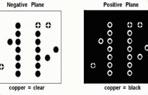
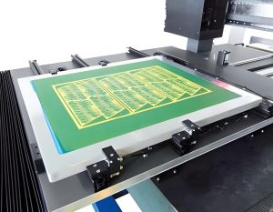
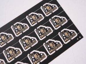
Laser direct imaging, or LDI, transfers PCB circuit and solder mask patterns directly from digital production data onto photosensitive material. Unlike conventional exposure, it does not rely on a physical film phototool. A laser direct imaging PCB workflow uses digital production data instead of a physical mask.
This gives the PCB manufacturer more control over image scaling, alignment, and panel distortion. The process is particularly useful for HDI boards, fine-line multilayer PCBs, flexible circuits, dense BGA designs, and boards with tight solder mask registration.
LDI is not necessary for every PCB. Conventional imaging may still be suitable for boards with wider traces, generous spacing, stable materials, and relaxed registration tolerances. The correct choice depends on the design rather than the layer count alone.
What Is Laser Direct Imaging (LDI)?
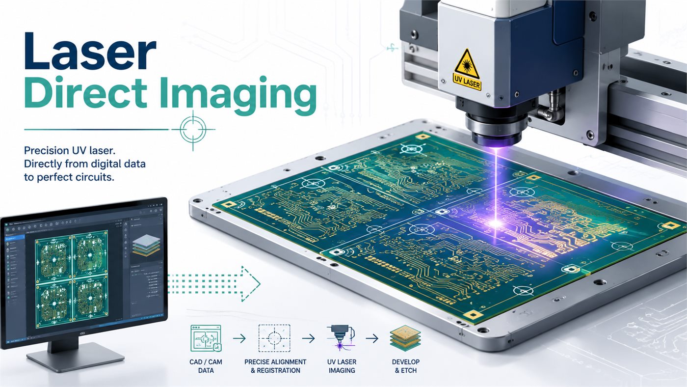
Laser direct imaging is a digital PCB exposure process. An LDI machine reads CAM data generated from Gerber or ODB++ files and exposes the required pattern directly onto photoresist or liquid photoimageable solder mask. A physical film mask is not required.
LDI may be used for:
- Inner-layer circuit imaging
- Outer-layer circuit imaging
- HDI build-up layers
- Pattern-plating processes
- Solder mask exposure
- Flexible and rigid-flex circuits
- Fine-line package substrates
LDI does not remove copper or drill holes. It creates the photosensitive pattern that controls later developing, etching, plating, or solder mask processing.
How Does Laser Direct Imaging Work?
The process begins with digital PCB artwork. CAM software converts the production data into exposure instructions for the LDI system.
Before imaging, registration cameras locate targets on the PCB panel. The machine compares their actual positions with the design coordinates and may correct:
- X-Y position
- Rotation
- Image scale
- Panel expansion or shrinkage
- Local dimensional distortion
The system then exposes selected areas of the photosensitive coating with controlled ultraviolet light. After exposure, the panel enters the developing process. Soluble resist is removed, leaving the required circuit or solder mask image.
This digital correction is one of the main reasons LDI is useful for advanced PCBs. Panels can change slightly during lamination, heating, copper plating, or flex-material processing. A fixed phototool cannot easily adapt to those changes, while an LDI image can be adjusted before exposure.
What Is the Step-by-Step LDI PCB Imaging Process?
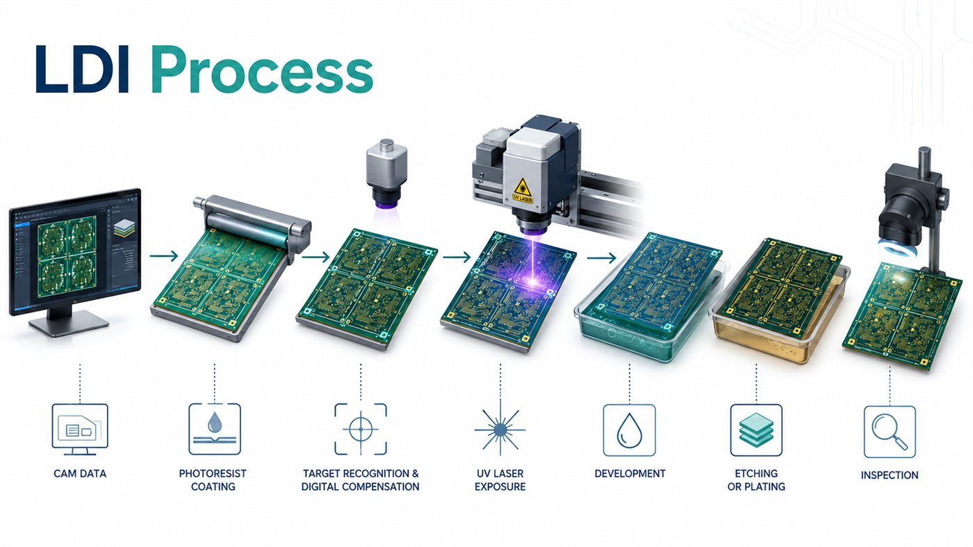
The exact workflow varies between inner layers, outer layers, and solder mask, but the main sequence is similar.
- CAM preparation: Engineers check layer polarity, panelization, tooling targets, scaling, and manufacturing compensation.
- Surface cleaning: Copper is cleaned and, when required, micro-etched. Dust, oxidation, oil, or fingerprints can weaken resist adhesion.
- Photoresist application: Dry-film photoresist is laminated onto copper. For solder mask, liquid photoimageable material is coated and tack-dried.
- Target recognition: Cameras locate tooling holes, etched targets, or fiducials on the panel.
- Digital compensation: Software adjusts the exposure image to match the actual panel dimensions.
- Laser exposure: The LDI system writes the circuit or solder mask pattern onto the photosensitive layer.
- Development: The soluble part of the resist is removed, revealing the required pattern.
- Etching or plating: Inner layers normally proceed to etching. Outer layers may enter pattern plating before final etching.
- Resist stripping: Temporary circuit resist is removed after completing its masking function.
- Inspection: AOI or solder mask inspection checks for opens, shorts, missing features, registration errors, and unwanted mask coverage.
LDI improves image placement, but it cannot correct poor cleaning, unstable development, excessive etching variation, or unsuitable photoresist.
What Are the Main Components of a Laser Direct Imaging System?
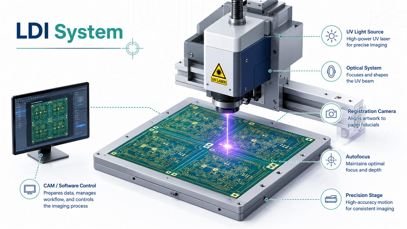
An LDI machine combines imaging, optical, motion-control, and data-processing systems. Its main components normally include:
- UV light source: Supplies exposure energy.
- Optical system: Directs and focuses the light.
- Image-modulation unit: Controls which areas are exposed.
- Registration cameras: Detect panel targets.
- Precision stage: Positions the panel or imaging head.
- Autofocus system: Adjusts for panel thickness and surface variation.
- CAM software: Converts PCB data into exposure instructions.
- Handling system: Loads, aligns, turns, and unloads panels.
- Environmental controls: Reduce dust, vibration, and temperature variation.
Equipment model alone does not prove manufacturing capability. PCB buyers should focus on stable line width, spacing, registration tolerance, supported materials, qualified resist systems, and volume-production performance.
What Photoresist Is Used for Laser Direct Imaging?
Circuit imaging usually uses dry-film photoresist designed for the wavelength and energy output of the LDI machine. A laser direct imaging photoresist must match the exposure wavelength and process energy. Liquid photoimageable materials are more commonly used for solder mask.
A suitable LDI photoresist should provide:
- Compatibility with the exposure wavelength
- Adequate photospeed
- Strong adhesion to prepared copper
- Resolution for the required line and space
- Resistance to etching or plating chemistry
- Clean developing and stripping
- Stable tenting over holes, when required
- A practical manufacturing process window
Common LDI systems operate with ultraviolet wavelengths such as 355 nm or 405 nm. Some equipment supports multiple wavelengths to improve compatibility with different resist systems.
The advertised resolution of a dry film should not be treated as the finished PCB capability. Actual production results also depend on copper surface roughness, resist thickness, lamination pressure, exposure energy, development control, copper thickness, and etching factor. The resist, equipment, and manufacturing process must be qualified together.
How Is Laser Direct Imaging Used for PCB Solder Mask?
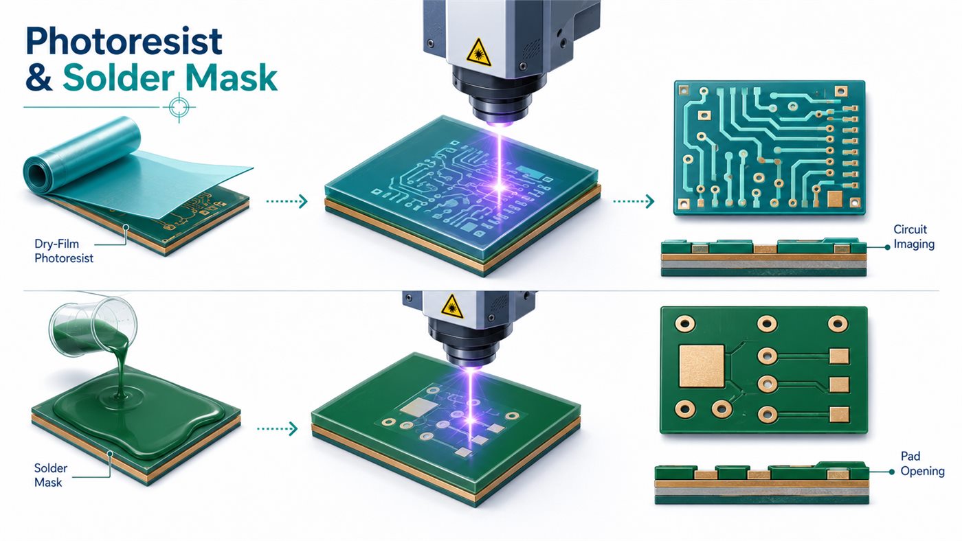
In a laser direct imaging solder mask process, the PCB is first coated with liquid photoimageable material and partially dried. The LDI system then aligns the digital solder mask pattern with the actual copper pads before exposure.
After developing, solder mask is removed from pads, holes, test points, and other required openings. LDI solder mask is particularly useful for:
- Fine-pitch BGA pads
- QFN and LGA footprints
- Small solder mask dams
- Dense connector pads
- Closely spaced test points
- Flexible circuits
- Boards with tight mask-to-pad registration
Because the image is aligned to the real panel, the manufacturer may not need to enlarge solder mask openings as much as with less accurate exposure methods. This can help preserve narrow dams between adjacent pads.
LDI does not remove the need for realistic design rules. Final solder mask openings still depend on manufacturer registration tolerance, coating thickness, solder mask chemistry, development control, surface finish, assembly requirements, and solder mask color. White, black, and other less-transmissive colors may require different exposure settings, so critical dams and colors should be specified during quotation.
Laser Direct Imaging vs Traditional Photolithography
The choice depends on whether the PCB needs digital compensation, tighter registration, or phototool-free processing.
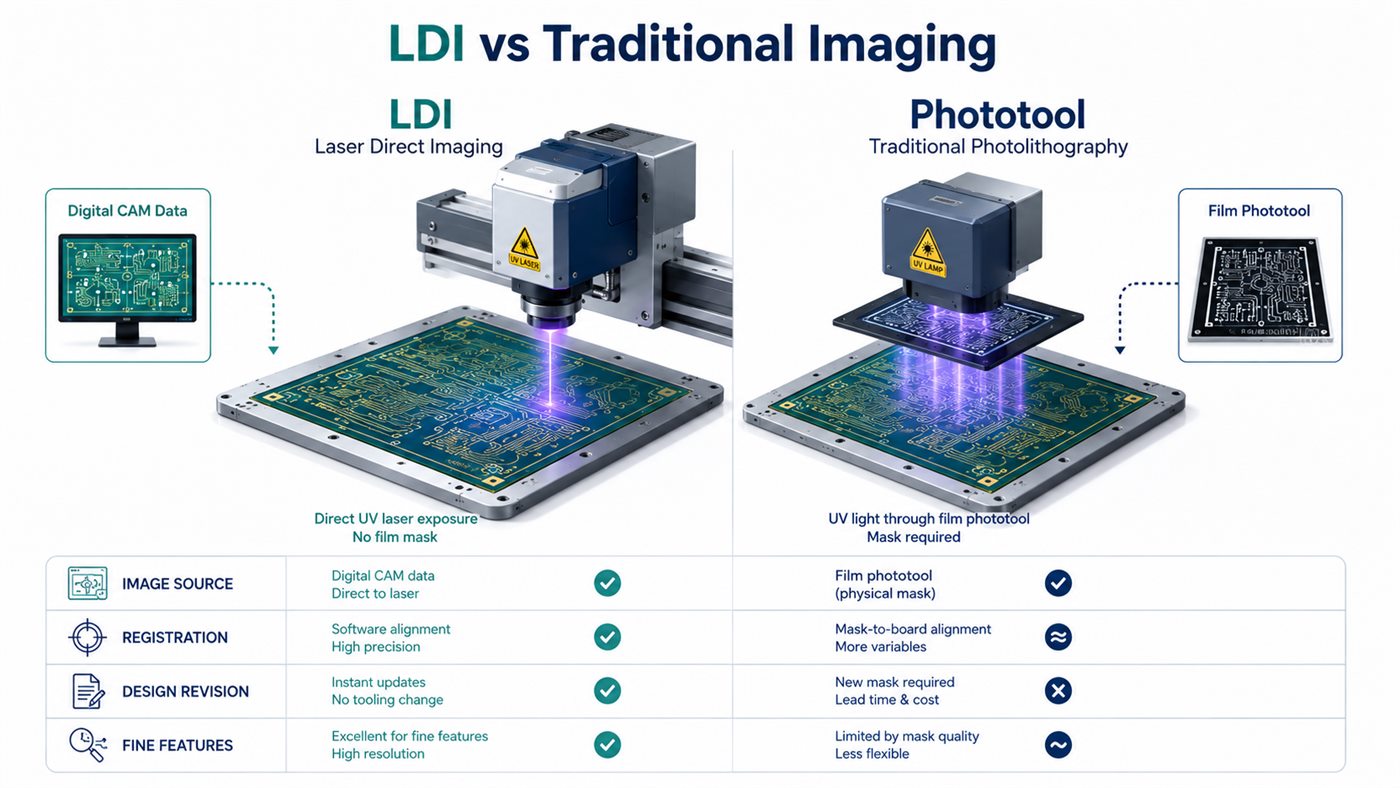
| Comparison Point | Laser Direct Imaging | Traditional Photolithography |
|---|---|---|
| Image source | Digital CAM data | Film or glass phototool |
| Physical mask | Not required | Required |
| Registration | Digitally corrected | Depends on film and tooling |
| Panel distortion | Can be compensated within process limits | More difficult to correct |
| Design revisions | CAM data can be updated | New film may be required |
| Fine features | Better suited to dense patterns | Suitable for conventional geometry |
| Prototype setup | No film preparation | Additional phototool preparation |
| Flex materials | Better compensation for dimensional movement | More dependent on fixed scaling |
| Equipment investment | Higher | Usually lower |
| Simple volume boards | May offer limited benefit | Often practical and economical |
Traditional imaging remains suitable when the board geometry is comfortably within the manufacturer’s process window. LDI becomes more valuable as trace, spacing, and registration margins become tighter.
What Are the Advantages of Laser Direct Imaging?
LDI provides practical benefits when imaging accuracy is a major manufacturing constraint:
- More accurate registration: The exposure image can be matched to the measured panel.
- Better fine-line support: Narrow traces, spaces, pads, and solder mask dams can be positioned more accurately.
- Faster engineering revisions: Updated artwork does not require a new film set.
- Fewer phototool defects: Film scratches, stretching, dust, and handling damage are removed from the process.
- Material compensation: Digital scaling helps with thin cores, flex materials, and sequentially laminated structures.
- Efficient prototype preparation: Small batches and revised designs can move into exposure without film production.
- Improved solder mask alignment: Openings can follow the actual copper pattern rather than the nominal panel position.
These advantages matter most when conventional imaging is close to its practical limits. LDI will not compensate for weak stack-up design, excessive etching variation, or unrealistic PCB tolerances.
What Are the Limitations of Laser Direct Imaging?
LDI equipment requires high capital investment, controlled production conditions, regular calibration, preventive maintenance, and trained operators.
Other limitations include:
- Exposure speed may drop with slow photoresist or dense image areas.
- Photoresist and solder mask must match the machine wavelength.
- Poor copper cleaning can still cause resist failure.
- Warped panels may exceed the autofocus or handling range.
- Uneven coating thickness can affect exposure results.
- Severe panel distortion cannot always be corrected.
- Fine imaging still depends on stable plating and etching.
- Simple PCBs may not gain enough benefit to justify the process cost.
For a standard double-sided PCB with wide traces and generous clearances, conventional exposure may provide the same usable result at a lower cost.
Which PCB Types Benefit Most from LDI?
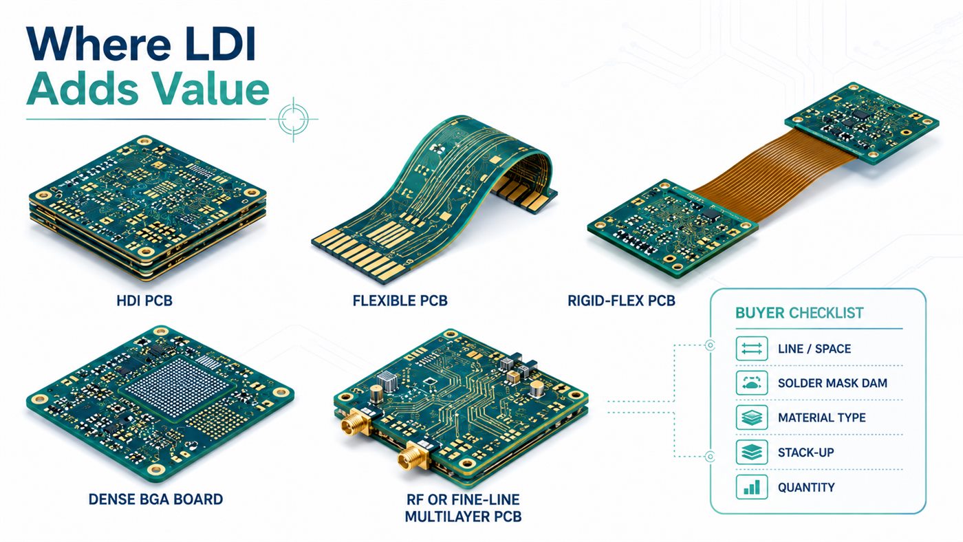
LDI provides the greatest value where feature density or material movement leaves little room for registration error.
| PCB Type | Why LDI Helps | Main Imaging Concern |
|---|---|---|
| HDI PCB | Supports dense build-up routing | Fine lines and small microvia pads |
| Fine-line multilayer PCB | Improves layer pattern placement | Narrow traces and annular rings |
| Flexible PCB | Compensates for material movement | Stretching and shrinkage |
| Rigid-flex PCB | Handles different material behavior | Uneven dimensional change |
| BGA breakout board | Supports dense fan-out routing | Fine spacing and mask dams |
| RF or microwave PCB | Preserves conductor geometry | Line-width accuracy |
| Package substrate | Supports very dense patterns | Fine features and registration |
| Prototype PCB | Simplifies design revisions | Repeated artwork changes |
A PCB does not need LDI simply because it has many layers. A high-layer-count board with conservative geometry may be easier to image than a thin four-layer flex PCB with tight solder mask registration.
When Should a PCB Design Require LDI?
LDI should be discussed when the design includes one or more of the following:
- Trace and space near the manufacturer’s conventional imaging limit
- Small annular rings
- Dense BGA fan-out
- Fine-pitch connector routing
- Small solder mask dams
- Tight solder mask-to-copper alignment
- Thin flex materials
- Sequential lamination
- Tight layer-to-layer registration
- Frequent prototype revisions
The design package should clearly state:
- Minimum line width and spacing
- Smallest annular ring
- Finished copper thickness
- Solder mask dam and color
- Material type and stack-up
- Impedance requirements
- Quantity and lead time
These values allow the PCB manufacturer to decide whether LDI is necessary, beneficial, or unnecessary.
What Affects LDI PCB Cost, Lead Time, and Manufacturing Yield?
PCB buyers rarely need to know the purchase price of the LDI machine. Their project cost is influenced more directly by exposure time, materials, panel utilization, process complexity, and expected yield.
- Trace and spacing: Features near the process limit require tighter control.
- Layer count: Each additional circuit layer adds imaging and inspection steps.
- Image density: Dense patterns may increase exposure time.
- Photoresist speed: Slower materials reduce equipment throughput.
- Solder mask detail: Small dams and tight openings require a narrower process window.
- Material stability: Flex and thin-core materials may require more compensation.
- Panel utilization: Poor nesting increases the cost per finished board.
- Inspection requirements: Fine-line designs may require more detailed AOI review.
- Yield risk: Designs combining several minimum features may require engineering trials.
LDI can shorten phototool preparation, but drilling, lamination, plating, surface finish, electrical testing, and material availability may have a greater effect on the final lead time.
How Should Buyers Evaluate a PCB Manufacturer’s LDI Capability?
Owning an LDI machine does not mean a supplier can produce every fine-line design reliably. Ask the manufacturer:
- What minimum trace and space are stable in volume production?
- Are the stated limits standard capability or prototype capability?
- What registration tolerance can be maintained?
- Is LDI used for inner layers, outer layers, solder mask, or all three?
- Which dry-film and solder mask materials are qualified?
- Can the process compensate for flexible-material movement?
- What registration targets are required?
- How are exposure focus and energy controlled?
- What inspection follows the imaging process?
- How is capability verified across the entire production panel?
For quotation, provide:
- Gerber or ODB++ data
- NC drill files
- Fabrication drawing
- Stack-up and material specification
- Finished copper thickness
- Impedance requirements
- Solder mask color and minimum dam
- Order quantity and delivery target
At EBest Circuit, we can review these details before quotation and determine whether LDI is required for the circuit pattern, solder mask, or both. This is more useful than requesting a specific equipment brand because the imaging method must match the complete PCB construction.
FAQs About Laser Direct Imaging
Q1. Is laser direct imaging the same as laser etching?
No. LDI exposes photosensitive material to form a pattern. Copper is removed later through chemical etching. Laser etching removes or changes material directly.
Q2. Does LDI remove copper from a PCB?
No. It defines the photoresist image. Etching or plating takes place in a later manufacturing step.
Q3. Can LDI be used for flexible PCBs?
Yes. Digital image compensation is useful for thin flexible materials that may expand, shrink, or distort during production.
Q4. Can LDI expose both dry film and liquid solder mask?
Yes, as long as the material is compatible with the machine wavelength and exposure energy.
Q5. What wavelength is used for PCB laser direct imaging?
Common systems use ultraviolet wavelengths such as 355 nm or 405 nm. Multi-wavelength equipment is also available.
Q6. Does every HDI PCB require LDI?
No. Some HDI boards can be produced with conventional exposure when their traces, spacing, annular rings, and registration tolerances remain within a stable process window.
Q7. Is LDI faster than traditional photolithography?
It removes film preparation, but exposure throughput depends on the machine, image density, panel area, resist sensitivity, and alignment method.
Q8. Does LDI improve PCB manufacturing yield?
It can improve yield when registration error or panel movement is a major defect source. Yield also depends on lamination, plating, development, etching, and inspection.
Q9. Can LDI compensate for panel expansion and shrinkage?
Yes, within the correction range of the equipment. Severe or irregular distortion may still make the panel unusable.
Q10. What files are required for LDI imaging?
The manufacturer normally needs Gerber or ODB++ data, drill files, a fabrication drawing, and stack-up information.
Q11. Is LDI suitable for prototype and volume production?
Yes. It supports fast artwork revisions for prototypes and is also used in volume production of HDI, multilayer, flex, and substrate products.
Q12. What is the difference between LDI and laser drilling?
LDI exposes photosensitive material. Laser drilling removes dielectric material to create microvias. They are separate PCB manufacturing processes.
Laser direct imaging is most useful when fine features, material movement, or registration requirements are difficult to control with conventional phototools. It can improve circuit imaging, solder mask alignment, and prototype revision efficiency, but it does not replace sound design rules or stable downstream processing.
For a manufacturing review, send your Gerber files, stack-up, quantity, minimum line and space, solder mask requirements, and delivery target to sales@bestpcbs.com. We can evaluate whether LDI is technically necessary and recommend a practical production route.