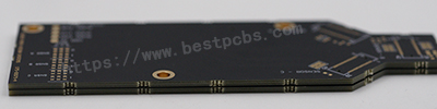
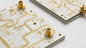
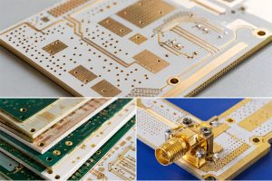
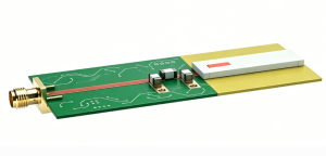
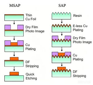
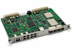
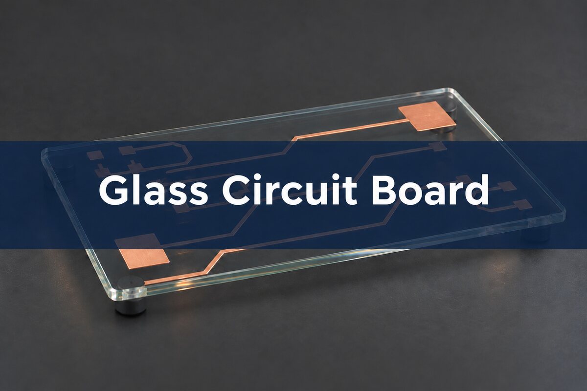
A glass circuit board can have a clear base and still have visible, opaque copper traces. If you need to see through the conductors too, you’re shopping for a transparent electrode, not simply a different board material. And if you only need a glass front panel, the circuit may not need to be built on glass at all.
Take a touch button next to a lit status window. Start by drawing the area that must transmit light. If the sensor can stay under an opaque border, a conventional board behind the glass is the first option to try. If an electrode has to cross the window, compare patterned indium tin oxide (ITO) with metal traces kept out of the viewing area. Then check both the electrical budget and the finished optical stack.
Glass Circuit Board: What Is Actually Made of Glass?
Ask for a cross-section before reading the supplier’s material name. Glass could be the cover your user touches, the rigid base that carries a conductor, or a core inside an advanced package. These are different parts. In the touch-button example, a cover glass over a separate PCB does not carry or route any electrical signal. A patterned electrode on the bottom of the cover does.
For a circuit built on solid glass, check whether the pattern is bonded copper, deposited metal, or a conductive coating. That choice determines whether you can see through a trace, how it connects to a cable, and whether it makes sense to mount any components on it. Don’t assume a clear substrate can go through your ordinary PCB soldering process.
PCB Glass Fiber: Why FR-4 Is Not a Solid Glass Board
FR-4 is a composite. Glass fabric reinforces the resin and copper is laminated to the resulting material. Isola’s 370HR data sheet, for example, describes an epoxy laminate made with E-glass fabric. The woven glass does not replace the resin or turn the assembly into an optical window.
A thin piece of uncoated laminate may pass some light and still be unsuitable for viewing a status icon, camera, or display. Scattering, copper patterns and surface finishes all affect what you see. If the board can sit behind a bezel, specify it as a conventional PCB and put the optical requirements on the separate glass assembly. Avoid buying a special conductor process to solve a cover problem.
Transparent PCB Material: Copper on Glass vs ITO vs FR-4
Pick the construction by the job the clear zone has to do. “Transparent” alone doesn’t tell you whether a trace can power a load, whether a touch pad will respond, or whether a customer can read an icon behind it.
| Construction | Choose it when | Check before release |
| Copper on glass | The spaces must stay clear but opaque traces are acceptable or can sit under a border. | Visibility of the copper pattern, metal adhesion and termination process. |
| Patterned ITO on glass | A sensing electrode overlaps a viewing area and needs to transmit light. | Sheet resistance, optical transmission and the contact to the flex or cable. |
| FR-4 PCB behind a glass cover | The window can remain clear by moving the wiring and components outside its sightline. | Mechanical stack, glass-to-sensor spacing and assembled touch response. |
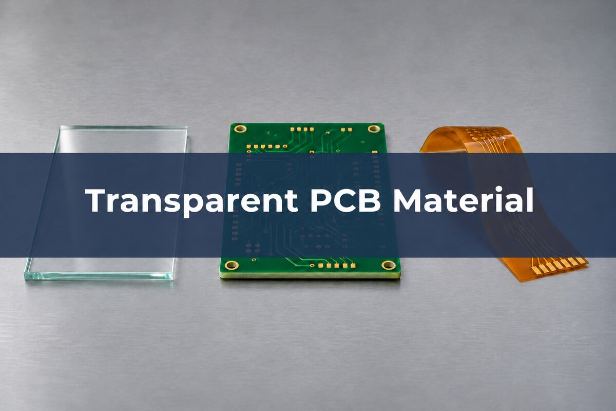
If opaque lines are allowed only outside the window, move power and ground to the opaque area first. Reserve the transparent conductor for functions that need it. If you need a flex connection, specify whether the flex body must also transmit light or just stay out of the view. An amber flex tail and a transparent electrode are not interchangeable.
ITO Glass Electrode: Parameters Worth Specifying
Start with sheet resistance in Ω/□, optical transmittance at the wavelength you care about, glass thickness and electrode dimensions. Add the coating side and the contact method. Ask the supplier to distinguish specified electrical values, typical optical curves and properties that will be measured on your finished part.
| Supplier example | Published value | How to use it |
| PG&O CEC020 S | ≤20 Ω/□ specified; 100 nm typical film | Screen a lower-resistance route; verify optics separately. |
| PG&O CEC100 S | 100 ±20 Ω/□ specified; 23 nm typical film | Use the high end of the range to screen voltage drop. |
| Optical transmission | Supplier’s typical curves measured at 0° incidence | Request a guaranteed limit and coupon geometry if it affects release. |
These values come from the PG&O ITO coating table and its transmission curves. They are examples for named products, not generic ITO values. The supplier describes those curves as typical, not production specifications. They also do not include your adhesive, printing, display or connector.
Sheet Resistance Formula: Check the Long, Narrow Segment First
For a uniform rectangular film with contacts spanning opposite ends, estimate film resistance as R = Rs × L/W. The length and width must use the same unit. A 24 mm path that is 3 mm wide has eight squares. With a 20 Ω/□ film, that is 160 Ω before the contact resistance. With a 120 Ω/□ upper bound, it is 960 Ω. The TU Wien thin-film measurement notes explain the square-film basis.
Here is a worksheet you can reuse for a DC branch from a window to a hidden connector. Assume 0.25 mA and a 50 mV budget for the whole path. That gives a 200 Ω limit. This is a screening example, not a touch-controller specification.
| Film and path | Film drop | What to do |
| 20 Ω/□, 24 × 3 mm | 40 mV | Only 10 mV remains for connections and other series losses. Verify the assembled path. |
| 120 Ω/□, 24 × 3 mm | 240 mV | Exceeds the example limit. Shorten the film path or route in metal outside the visible area. |
| 20 Ω/□, 24 × 6 mm | 20 mV | More electrical margin, but check the wider feature’s effect on the window. |
Enter the longest actual path, the narrowest designed width and the relevant sheet-resistance limit. If a line tapers or pinches, check its segments separately; a single average width can miss a bottleneck. The simple calculation leaves out contact resistance and current spreading at small terminals. For a capacitive touch electrode, verify the controller’s scan behavior and touch response as well; the DC estimate alone does not establish sensitivity.
Through Glass Vias: When You Need a Back-Side Connection
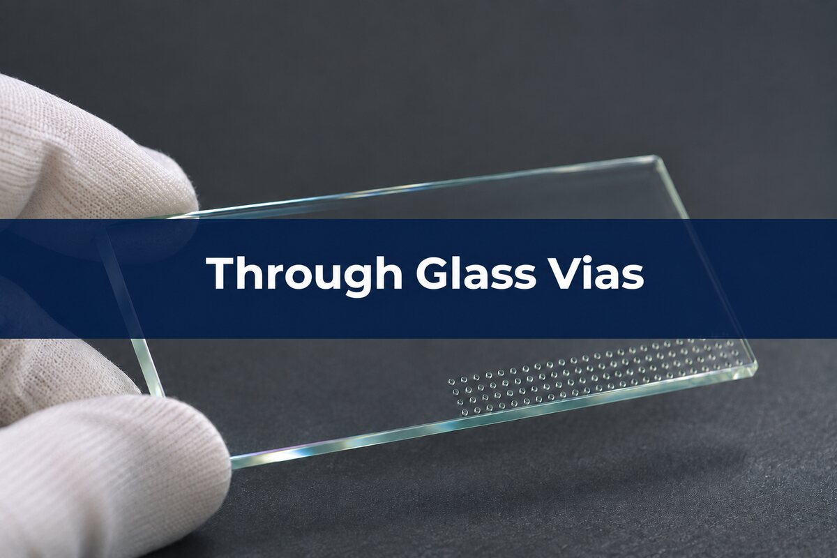
A through-glass via (TGV) is an opening through solid glass. A bare hole does not conduct; the finished electrical structure needs a specified metallization or fill and an interface to the surface wiring. A TGV is useful where a routed connection really must exit the back. It is not necessary for a one-sided electrode that can be contacted at the edge.
For scale, Corning’s August 2018 TGV product sheet lists 30–100 µm via diameter and 100–500 µm wafer thickness for its described offering. These are portfolio figures, not proof that every diameter works at every thickness or that the hole is supplied metal-filled. Ask for the supported combination, finished connection, sectioned sample and applicable electrical evidence. See the separate glass-core substrate guide for packaging uses.
Optical Transmittance Measurement: Read the Finished-Stack Report
Check the sample description before the percentage. The report should say whether it covers bare glass, coated glass, or the assembled window. Also look for the wavelength or wavelength band, incidence angle, the measured area and the optical method. Compare a measurement through the patterned zone with a control area if the user will see both.
Suppose the project calls for at least 85% transmission at 550 nm and normal incidence through a particular viewing zone. A report of 88% at 550 nm on the bare blank does not release the patterned window. Ask for the result on the actual glass, coating and adhesive stack at the specified location and conditions. If haze or contrast matters to legibility, define a separate criterion instead of assuming high transmission proves a clear image. The 85% value belongs to this example, not an industry minimum.
Capacitive Touch Sensor Through Glass: Validate the Assembly
Build the trial with the final glass thickness and adhesive. A normal bench touch on a bare board doesn’t tell you what will happen behind the window. The Texas Instruments CapTIvate design guide, Revision B, explains how overlay thickness, dielectric properties and air gaps affect the field at the sensing surface.
Start with the simplest build: an electrode behind the opaque border where the user can still touch it. If the sensor works there, you may not need ITO at all. If the electrode has to sit in the clear zone, compare the patterned film with the first build on the same controller settings. Log no-touch readings, touch delta and false triggers with the display off and on. Test the intended use conditions, such as a gloved finger or a damp surface when required. Release against your controller and product criteria, not a single successful tap on an open bench.
Glass Circuit Board FAQs
Can I make the copper traces invisible by using thinner glass?
No. Thinner glass does not make a copper trace transparent. Change the conductor or keep copper outside the sightline.
Is a translucent FR-4 board clear enough for a display?
Don’t assume so. Check contrast and haze on the actual assembly, or place the PCB where it does not obstruct the display.
Can an ITO electrode power an LED?
Calculate the drop from the sheet resistance, path geometry and LED current first. If that consumes too much of the supply budget, feed the LED with metal conductors outside the visible zone.
Can I solder a wire directly to ITO-coated glass?
Don’t specify ordinary PCB soldering without qualifying the coating and contact process. Ask about a compatible terminal, conductive bond, or flex connection.
Does double-sided ITO glass connect the two sides?
No. Two conductive surfaces are not a connected two-layer circuit. A via, edge connection or separate contacts are needed according to your circuit.
Can I check sheet resistance by touching a multimeter to two points?
A two-point reading includes contact effects and depends on the geometry. Ask for a defined sheet-resistance method, such as a four-point probe measurement with appropriate geometry corrections.
Does a high transmittance reading mean the conductor pattern is invisible?
Not necessarily. The eye may still see pattern edges or a change in reflection. Compare printed and unprinted areas under the intended lighting and viewing angle.
What drawing should I send a transparent-electrode supplier?
Mark the optical zone, coating side, electrode and contact pattern. Include outline tolerances, maximum resistance, and any transmission or haze limit with its measurement conditions.
Technical References
- PG&O ITO coating specifications
- Corning TGV product information (August 2018)
- Texas Instruments capacitive touch design flow, Rev. B
Custom Glass PCBs with Free DFM Review
Need a glass circuit board built to your drawings? Send your files to EBest Circuit for a free design-for-manufacturing (DFM) review. We’ll check the proposed construction and flag details that need to be resolved before quoting or production.
Request a quote: Email sales@bestpcbs.com with your board drawing, circuit artwork and quantities. Include the glass type or thickness if already specified, along with any optical, electrical or assembly requirements that matter to your design.