An IPC-356 netlist gives PCB manufacturers a reference for which board connections belong together and which must remain separate. Comparing that reference with the copper and drill data can reveal a missing connection or unintended short before fabrication. After manufacturing, the connectivity data also supports electrical testing of the physical bare board.
EBest Circuit supports PCB fabrication, manufacturing-data review and bare-board electrical testing, with component sourcing and PCBA assembly available for the next stage. If your board is ready for fabrication, send your manufacturing files to sales@bestpcbs.com to discuss the build and its electrical test requirements.
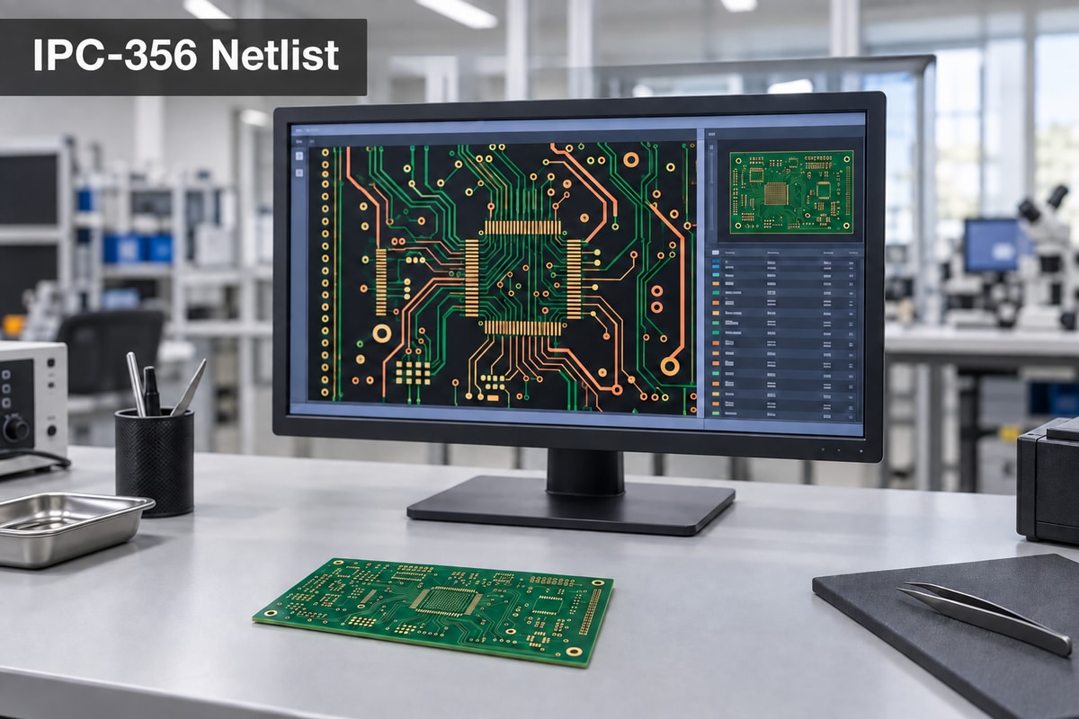
What Is an IPC-356 Netlist?
An IPC-356 netlist is a standardized text file that describes the electrical connectivity of a PCB. A net is a group of connection points intended to share the same electrical connection, such as a ground network or a signal running between two component pads.
The file associates those points with physical information, including their locations on the board. This lets manufacturing software relate an electrical connection to an actual pad, hole or accessible test location.
For example, if connector pin J1-1 and component pad R1-1 belong to the same net, the bare PCB should provide a conductive path between them. A nearby pad on a different net should remain electrically separate unless the design includes an intentional connection.
The name is often shortened to IPC-356, while PCB software may label the export IPC-D-356 or IPC-D-356A. It is a manufacturing and test-data format, not a complete PCB design file. It does not replace the copper artwork, drill files or fabrication drawing.
How Does the IPC-D-356 Netlist Format Describe PCB Connections?
The IPC-D-356 netlist format uses structured text records to identify connection points and their net membership. The fields let CAM and test software locate those points without opening the original PCB design application.
| Information | What it identifies |
|---|---|
| Net name | The electrical network assigned to a point |
| Reference and pin | The component location and pin or pad identifier, where applicable |
| X and Y coordinates | The point’s position on the PCB |
| Access information | The board side or layer information used to locate the connection |
| Pad and hole details | Physical features associated with the point, where exported |
Think of the file as a connectivity map rather than a drawing of every copper track. Two pads may be far apart and connected through several layers, yet still belong to one net. The netlist identifies their relationship; the copper and plated-hole data describe the physical route.
A simple example: J1-1 and R1-1 are assigned to SIGNAL_A, while J1-2 is assigned to GND. A comparison should find J1-1 connected to R1-1 and separate from J1-2. If the extracted copper network combines all three, it disagrees with the intended grouping.
That example describes the meaning of the records, not the literal file syntax. Actual records use defined field positions, so manually changing spacing or identifiers can make the file unreadable or alter its meaning. Regenerating the export from the PCB design is safer than editing it as ordinary text.
Why Compare an IPC Netlist with Gerber and Drill Data?
The comparison checks whether the manufacturing geometry preserves the connectivity in the PCB design. It is especially useful because a board can look correct in a Gerber viewer while containing an electrical discrepancy.
CAM software reads the copper layers and drill information, then extracts the networks formed by connected copper and plated holes. It compares that result with the separately exported CAD netlist.
The two references answer different questions:
- CAD netlist: Which connection points are assigned to the same net?
- Gerber and drill extraction: Which points are actually joined by the supplied manufacturing geometry?
Suppose an exported copper layer is missing a short track between two pads. The CAD netlist still groups those pads together, but the extracted network separates them. The disagreement reveals the missing connection before a board is manufactured.
If both the test reference and the board artwork come only from that same incomplete Gerber dataset, they may agree with each other. That agreement does not establish that they match the original design.
Gerber X2 can carry attributes, including net-related information where supported. Even so, the value of a separate CAD export is its independent reference path. It helps expose export or interpretation errors; it does not prove that an incorrect circuit connection already present in the design is functionally correct.
How Do You Export an IPC-356 Netlist from Altium Designer?
In Altium Designer, an IPC-D-356A file can be generated through a Test Point Report fabrication output. An Output Job keeps that export alongside the other manufacturing outputs for the same PCB document.
Using an Output Job:
- Open the project’s Output Job file, or add one if none exists.
- Under Fabrication Outputs, add Test Point Report and select the intended PCB document as its data source.
- Open the output’s configuration to display Fabrication Testpoint Setup.
- Enable IPC-D-356A as an output format.
- Connect the output to a folder container and set the destination and filename.
- Generate the output and locate the resulting IPC file.
Altium also provides a direct route through File > Fabrication Outputs > Testpoint Report in the PCB editor. Menu wording can vary by software version.
Generate the netlist from the same released PCB revision as the Gerber and drill files, after the copper pours and design changes are finalized. Otherwise, a valid file from an older revision can produce mismatches against the new artwork.
An exported file is not itself a successful netlist comparison. The comparison happens after the manufacturing layers, hole data and IPC netlist are imported and interpreted together. For boards with blind or buried vias, missing drill spans or an incorrect layer setup can change the extracted connectivity.
What Causes Netlist Mismatches, Opens and Shorts?
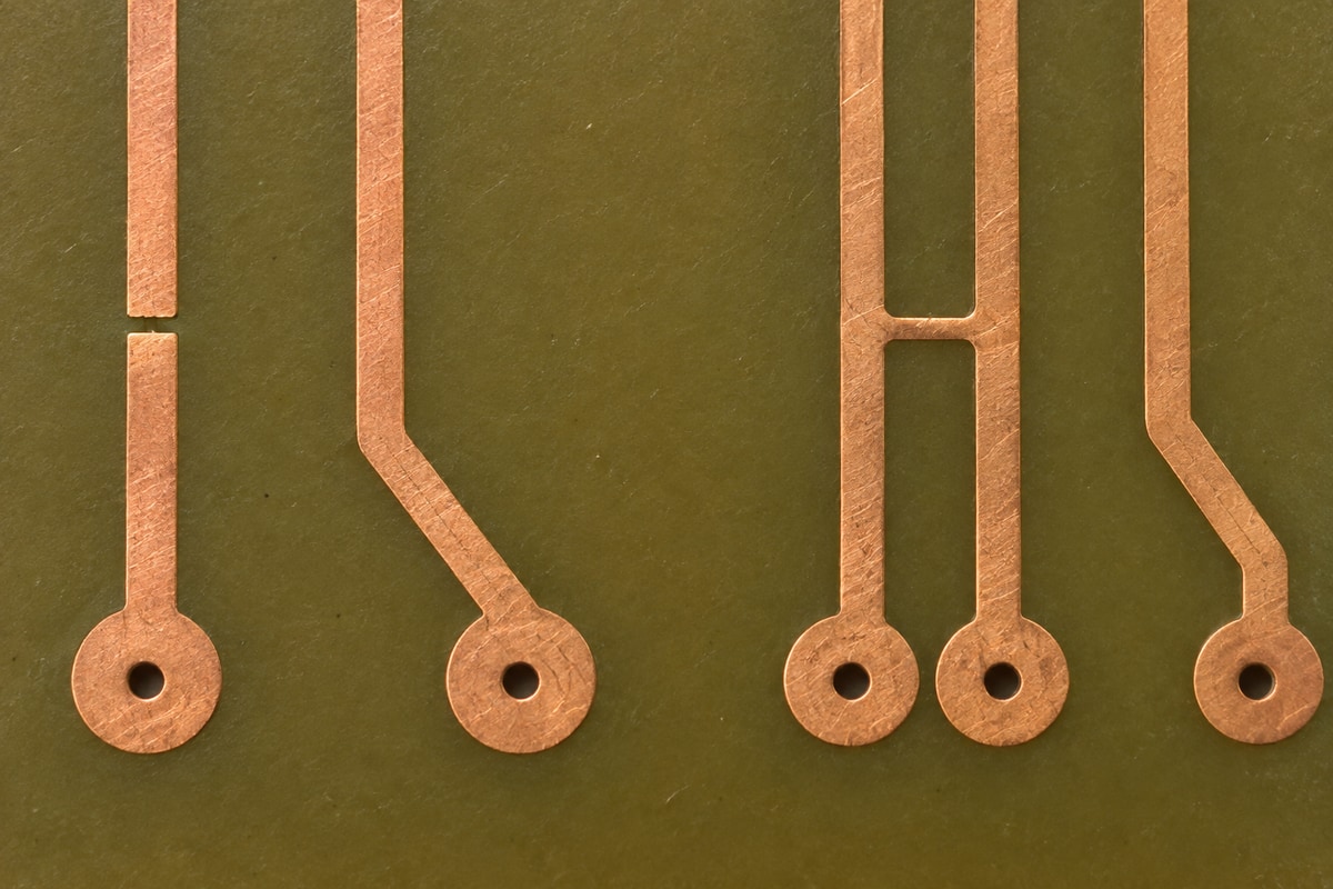
A netlist mismatch means two descriptions of the board disagree. It may reveal a real copper error, but it can also result from mixed revisions or an incorrect CAM import. The mismatch needs to be understood before it is treated as a board defect.
| Cause | How it appears in the comparison |
|---|---|
| Missing track or copper connection | One intended net is split into separate networks |
| Unintended copper bridge | Two intended nets become one connected network |
| Incorrect layer polarity or copper interpretation | Plane connections differ from the design reference |
| Missing or incorrectly assigned plated-drill data | Connections between layers appear absent or incorrect |
| Netlist and artwork from different revisions | Changed pads or nets no longer correspond |
| Intentional net tie | Differently named nets are physically joined by design |
An open breaks an intended path. In the manufacturing data, this may be a missing track or an unconnected plane feature. On a finished board, a broken conductor or defective plated connection can create an open even when the source files were correct.
A short joins paths that should be separate. It may exist in the supplied artwork or arise during fabrication. File comparison addresses the former; electrical testing of the manufactured board addresses the latter within the test’s coverage.
Not every missing-net message represents an open. Some extraction tools omit isolated single-node features or handle no-net objects differently. Likewise, an intentional net tie can join separate logical names without being an unwanted short. Reviewing the reported locations and the corresponding copper distinguishes these cases from genuine errors.
How Is an IPC-356 Netlist Used for Bare-Board Electrical Testing?
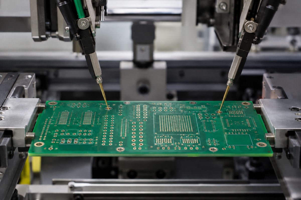
An IPC-356 netlist supplies connectivity information used to prepare a bare-board electrical test program. The equipment then measures the manufactured board rather than merely comparing files.
The main electrical checks are:
- Continuity: Does a path that should conduct meet the specified resistance limit?
- Isolation: Do networks that should remain separate meet the specified insulation-resistance requirement under the test conditions?
Flying-probe equipment moves probes between accessible locations without a dedicated bed-of-nails fixture. Fixture-based testing uses an array of contacts made for the board and can suit repeat production where fixture cost is justified. Both approaches depend on suitable access and a correctly prepared test program.
The netlist is only part of that preparation. Test voltage, resistance thresholds, probe access and coverage also affect what the test can establish. The existence of an IPC file alone does not define these settings or guarantee complete coverage.
This is why CAM comparison and bare-board electrical testing complement each other. The first can find an error in the manufacturing dataset before production. The second can find a physical connection defect introduced while making the board.
A passing bare-board test does not establish assembled-product performance. Component values, soldered assembly connections, firmware behavior and signal quality require the relevant PCBA inspections or functional tests.
Can ODB++ or IPC-2581 Replace a Separate IPC Netlist?
Yes, when the exported package contains the required connectivity and the manufacturer’s CAM and test workflow can use it. ODB++ and IPC-2581 can combine physical board information and logical connectivity in a richer manufacturing dataset.
| Manufacturing package | How connectivity is supplied |
|---|---|
| Gerber and drill files with IPC-D-356 | A separate netlist accompanies the manufacturing geometry |
| ODB++ | Net information can be included within the manufacturing package |
| IPC-2581 | Connectivity can be included in the structured manufacturing data |
An integrated package can reduce the need to match several separately exported files. However, the format name alone does not prove that the export contains all the data needed downstream. Export settings and the receiving software still matter.
A separate IPC netlist may therefore remain useful even when an integrated format is supplied, particularly when it provides an additional CAD-derived comparison reference. Whichever package is used, matching revisions and correctly interpreted connectivity matter more than the filename extension.
FAQs About IPC-356 Netlist
1. Is IPC-356 the same as IPC-D-356A?
IPC-356 is commonly used as shorthand when discussing this family of PCB netlist formats. IPC-D-356A is a specific designation that may appear in the export settings. Use the version supported by the receiving CAM or test system rather than assuming every variant is interchangeable.
2. Can I open an IPC-356 netlist in a text editor?
Yes. It is a text-based file, so a text editor can display its records. A compatible CAM viewer is more useful for relating those records to board locations. Opening the file successfully does not confirm that its contents are correct.
3. Can an IPC netlist be generated from Gerber files?
CAM software can extract connectivity from correctly interpreted Gerber and drill data and may export that result as an IPC netlist. However, a Gerber-derived netlist is not an independent record of the original CAD connectivity. An artwork error may be reproduced in the extracted netlist.
4. Does an IPC-356 netlist include the BOM?
No. References and pin identifiers associate connection points with board features, but they do not replace a bill of materials. Component values, manufacturer part numbers and procurement information belong in the assembly documentation.
5. Do I need a new netlist after changing the PCB layout?
Export a new netlist with the revised manufacturing files. Even when the circuit connections are unchanged, moved pads or altered vias can change the physical information used in comparison and test preparation. Keeping the files together as one revision avoids comparing different versions of the board.
Preparing your next PCB build? Send your manufacturing package and IPC-356 netlist, if available, to sales@bestpcbs.com. EBest Circuit can help review the fabrication data and plan bare-board electrical testing before the boards move into assembly.