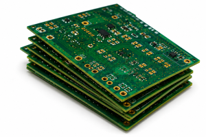
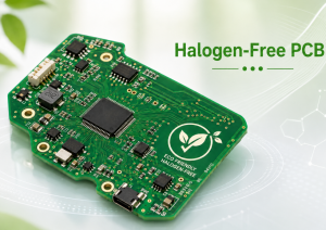
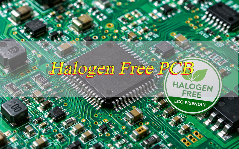
A halogen free PCB is normally specified by limiting chlorine and bromine in the base material, then controlling every additional material covered by the customer requirement. IEC 61249-2-21 is a common starting point for non-halogenated epoxy glass laminate, while test reports, material declarations, approved material grades, and drawing notes determine whether a production lot can actually be accepted.
This guide focuses on verification rather than repeating a general material overview. It explains the numerical limits, the difference between chemical and flammability requirements, the evidence a buyer should request, and the checks that should be completed before releasing a board for production.
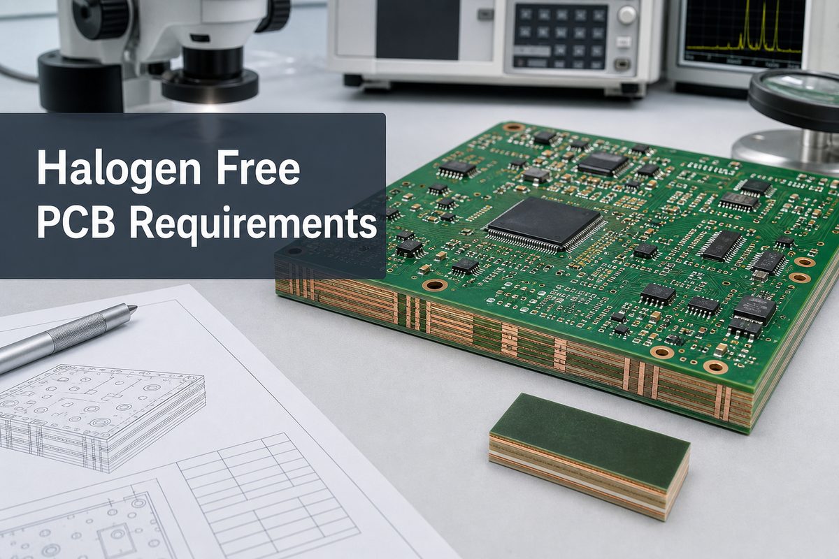
What Are the Core Halogen Free PCB Requirements?
The core chemical limits commonly used for halogen-free PCB laminate are chlorine at no more than 900 ppm, bromine at no more than 900 ppm, and the combined total at no more than 1,500 ppm. These limits are associated with IEC 61249-2-21 and should be applied to the exact material scope stated in the purchase specification.
| Requirement | Common Limit or Evidence | What It Covers |
| Chlorine content | ≤ 900 ppm | Chlorine in the tested base material |
| Bromine content | ≤ 900 ppm | Bromine in the tested base material |
| Combined chlorine and bromine | ≤ 1,500 ppm | Total of the two measured elements |
| Flammability | Specified material rating, often UL 94 V-0 | Burning behavior at the qualified thickness |
| Material identity | Approved grade and manufacturer | The laminate and prepreg actually used |
The limits do not mean the material contains absolutely zero halogen. They establish maximum measured concentrations. The drawing should therefore name the applicable standard, approved laminate grade, required flame rating, and evidence needed for lot acceptance.
Why Is Halogen Free Important?
Halogen-free requirements matter when an OEM must control restricted material chemistry, product environmental policy, combustion by-products, or supply-chain declarations. The requirement is most useful when it is tied to a defined product or customer specification rather than treated as a general synonym for “environmentally friendly.”
For engineers and buyers, the practical benefits are traceability and design control. A clear requirement reduces the chance of an unapproved laminate substitution, establishes which materials need declarations, and makes prototype-to-production transfer easier. For a broader explanation of the terminology and applications, see our halogen-free PCB overview.
How Do IEC, RoHS, REACH, and UL 94 Differ?
IEC 61249-2-21, RoHS, REACH, and UL 94 answer different compliance questions, so passing one does not prove the others. A procurement specification should list each required condition separately.
| Reference | Primary Scope | Decision It Supports |
| IEC 61249-2-21 | Non-halogenated epoxy glass base materials | Material composition and base-material properties |
| IPC-TM-650 2.3.41 | Total halogen test method for base materials | How chlorine and bromine are measured |
| RoHS | Ten restricted substances in electrical and electronic equipment | Whether regulated substances meet applicable limits |
| REACH | Chemical obligations, including Candidate List substances in articles | Supply-chain communication and substance obligations |
| UL 94 | Small-scale flammability behavior of plastic materials | Whether the material has the specified flame classification |
A board can be RoHS compliant without meeting a customer’s halogen-free definition because RoHS restricts specific substances, including PBB and PBDE, rather than all chlorine and bromine content. Likewise, UL 94 is a flammability classification, not a complete chemical-composition declaration. Our RoHS information page provides additional context for projects that require both controls.
Which Materials Must Be Covered by the Requirement?
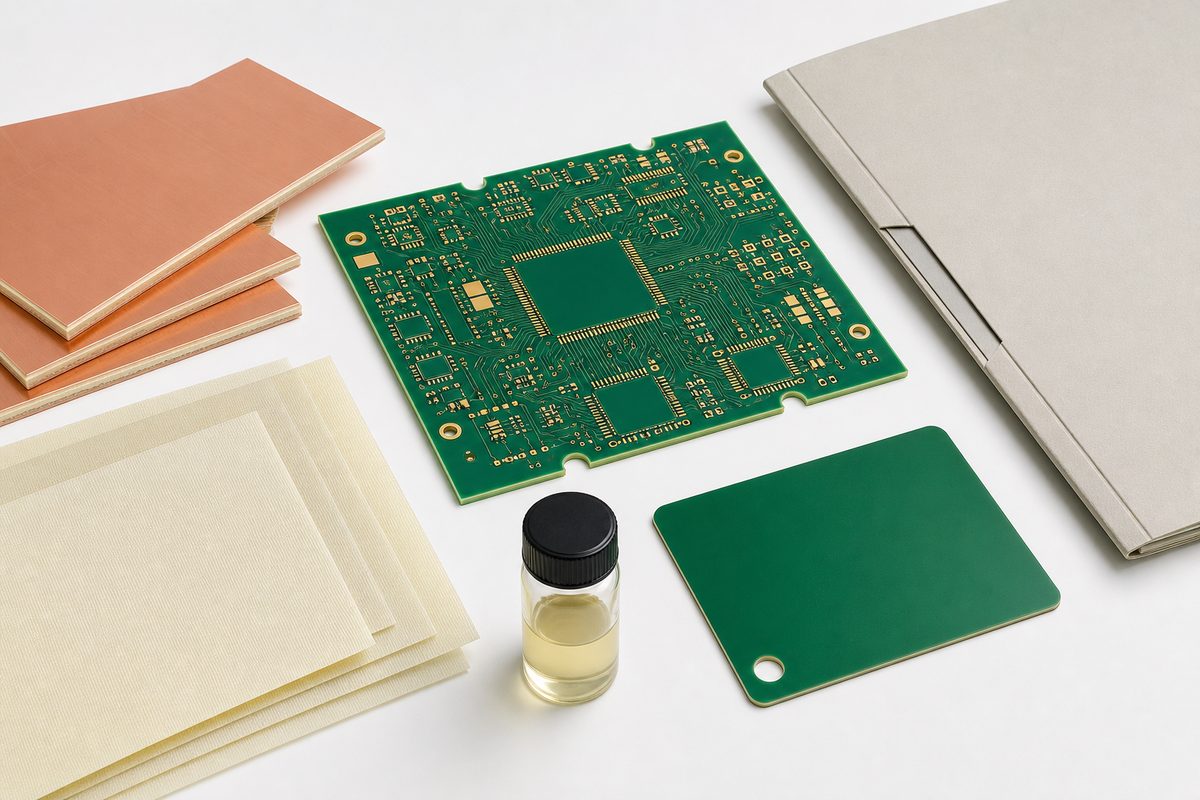
The required scope should include every material named by the customer specification, not only the laminate core. A narrow base-material requirement and a finished-PCB requirement are not automatically equivalent.
- Laminate cores and prepregs: confirm the exact manufacturer, grade, thickness, resin system, and supporting declaration.
- Solder mask and legend ink: request declarations when the customer requirement covers the finished bare board.
- Bonding films and adhesives: include them for flex, rigid-flex, heat-spreader, or other bonded constructions when applicable.
- Plugging, filling, and coating materials: review via-fill resin, peelable mask, carbon ink, and conformal coatings when they remain in the delivered product.
- Assembly materials: solder paste, flux, wire insulation, connectors, and component packages require separate PCBA-level control if the finished assembly is in scope.
The phrase halogen free pcb material is therefore too broad for a purchasing drawing unless the controlled materials are listed. The same applies to halogen free pcb laminate: a compliant laminate does not, by itself, document every material added later. Our detailed halogen-free PCB material guide explains the main laminate families and engineering properties.
How Should Halogen Free PCB Requirements Be Written on Drawings?
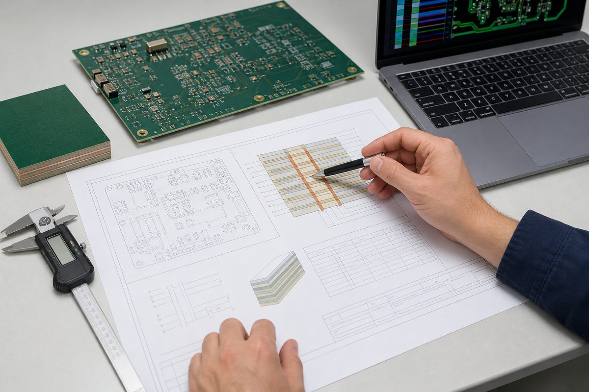
A useful fabrication note names the standard, material scope, approved grade or equivalency rule, flame rating, assembly compatibility, and required documentation. A note that only says “halogen-free FR4” leaves too many decisions open.
An example starting point is:
“Use halogen-free laminate and prepreg compliant with IEC 61249-2-21: Cl ≤ 900 ppm, Br ≤ 900 ppm, and Cl + Br ≤ 1,500 ppm. Material shall meet the specified UL 94 rating at the finished construction thickness. Supplier substitution requires written approval. Provide material declaration and certificate of conformity with the shipment.”
This example must be adapted to the product specification. The drawing may also need the laminate manufacturer and grade, IPC-4101 slash sheet, Tg, Td, Z-axis CTE, Dk/Df targets, copper foil type, lead-free assembly requirement, and lot traceability. Designers can also compare available rigid-board material options on our FR4 PCB page.
Which Documents Should a Supplier Provide?
The documentation package should prove material identity, declared composition, and production traceability at the level required by the contract. A generic marketing statement is not enough for controlled projects.
- Material declaration: identifies the applicable laminate or material family and its declared halogen status.
- Technical data sheet: provides Tg, Td, CTE, Dk/Df, moisture absorption, flammability, and other grade-specific properties.
- Certificate of conformity: links the delivered product to the purchase order and specified requirements.
- Lot or batch traceability: links incoming material, production traveler, and shipment records.
- Test report: provides measured chlorine and bromine results when contractually required.
- Change notification: prevents silent substitution of the laminate, prepreg, solder mask, or other controlled material.
The buyer should also define whether documents are needed with every lot, only for first-article approval, or upon request. That decision affects administration time, test cost, and release lead time.
How Is Total Halogen Content Tested?
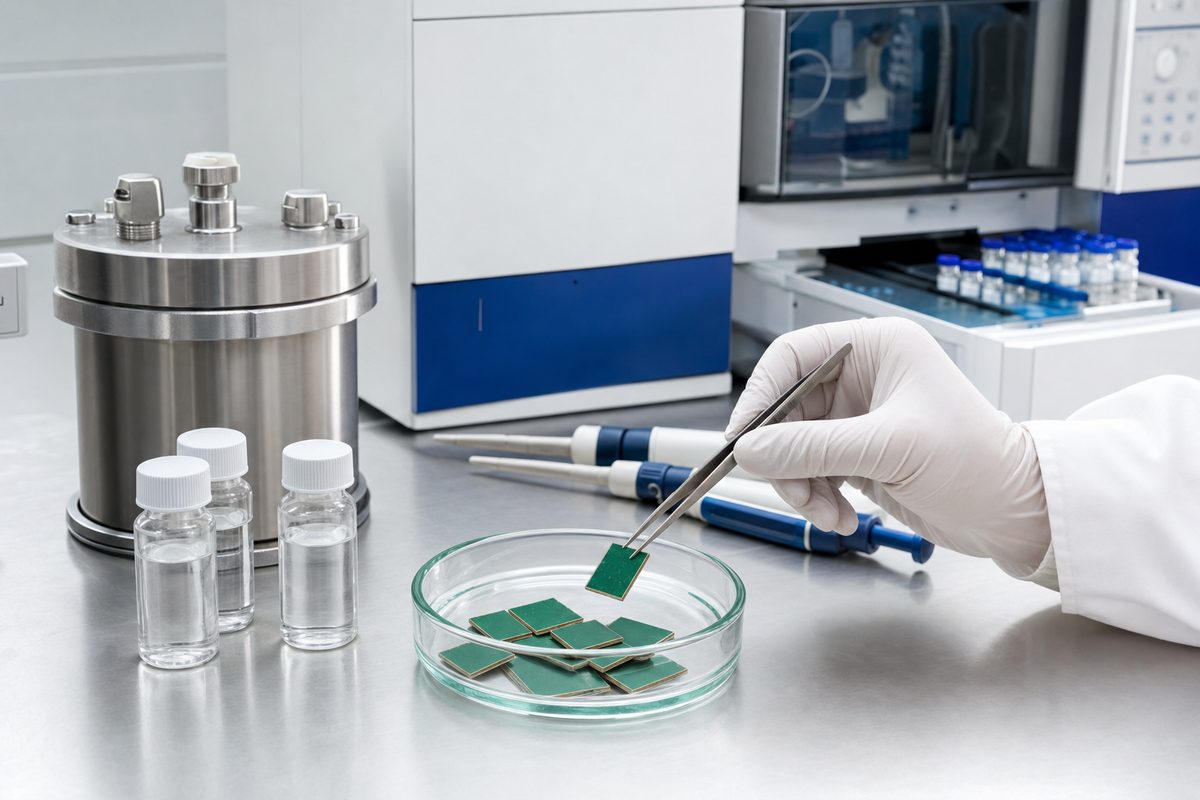
Total halogen testing for base materials commonly uses combustion sample preparation followed by ion chromatography to quantify chlorine and bromine. IPC-TM-650 2.3.41 describes a total-halogen method for base materials; surface ionic contamination methods answer a different question.
- A representative material specimen is selected and weighed.
- The specimen is combusted so chlorine- and bromine-containing compounds are converted into measurable ions.
- The combustion products are absorbed into a prepared solution.
- Ion chromatography separates and measures chloride and bromide.
- The laboratory reports results in ppm and compares them with the specified limits.
XRF screening can help identify elevated bromine or chlorine in some materials, but it may not provide the same compound-specific or low-level quantitative evidence as the contract test method. The test plan should state the sample type, preparation method, laboratory method, reporting limit, and acceptance criteria.
What Engineering Trade-Offs Need Review?
A halogen-free designation does not establish electrical, thermal, or mechanical suitability. Engineers still need to qualify the selected grade against the stackup, assembly profile, operating environment, and reliability target.
- Thermal behavior: compare Tg, Td, T260/T288, and Z-axis CTE with the expected reflow and repair cycles.
- Drilling and desmear: filler content and resin chemistry can change tool wear, smear behavior, and hole-wall preparation.
- Signal performance: confirm Dk, Df, resin content, and glass style for controlled-impedance or high-speed designs.
- CAF and moisture performance: review laminate data and construction spacing for humid or high-bias applications.
- Availability: approved grades, prepreg styles, and copper-clad thicknesses may affect material lead time and substitution risk.
- Cost: special testing, lot-specific documentation, and restricted material choices may add cost beyond the laminate price.
The safest selection is not simply the grade with the highest Tg. It is the grade whose complete property set and processing history fit the actual board design.
What Should Be Checked Before Production Release?
Production should be released only after the drawing, stackup, approved materials, compliance evidence, and change-control path agree. The following checks prevent most avoidable specification gaps:
- The standard and numerical halogen limits are written on the controlled drawing or specification.
- The material scope is defined: laminate only, finished bare PCB, or complete PCBA.
- The laminate manufacturer, grade, prepreg styles, and acceptable equivalents are approved.
- UL 94, RoHS, REACH, and customer-specific requirements are listed separately.
- Tg, Td, CTE, Dk/Df, CAF, moisture, and lead-free assembly needs have been reviewed.
- Required documents and their delivery frequency are stated on the purchase order.
- Substitutions and supplier changes require written approval.
- First-article or third-party testing is defined when declarations alone are insufficient.
These checks turn halogen free PCB requirements into an auditable production instruction instead of an informal preference.
FAQ About Halogen Free PCB Requirements
Does halogen-free mean zero chlorine and bromine?
No. In common PCB specifications, halogen-free means the measured chlorine, bromine, and combined total remain below defined limits. It is a threshold-based requirement, not a claim that every halogen atom has been eliminated.
Is a RoHS-compliant PCB automatically halogen-free?
No. RoHS restricts ten named substances, including PBB and PBDE, but it does not set a universal limit for all chlorine and bromine in PCB materials. Halogen-free and RoHS requirements should be specified and documented separately.
Does UL 94 V-0 prove a laminate is halogen-free?
No. UL 94 V-0 describes flammability behavior under a defined small-scale test. It does not provide a full chemical-composition result. Use material declarations or the specified chemical test evidence to verify halogen content.
Can a standard FR4 PCB be halogen-free?
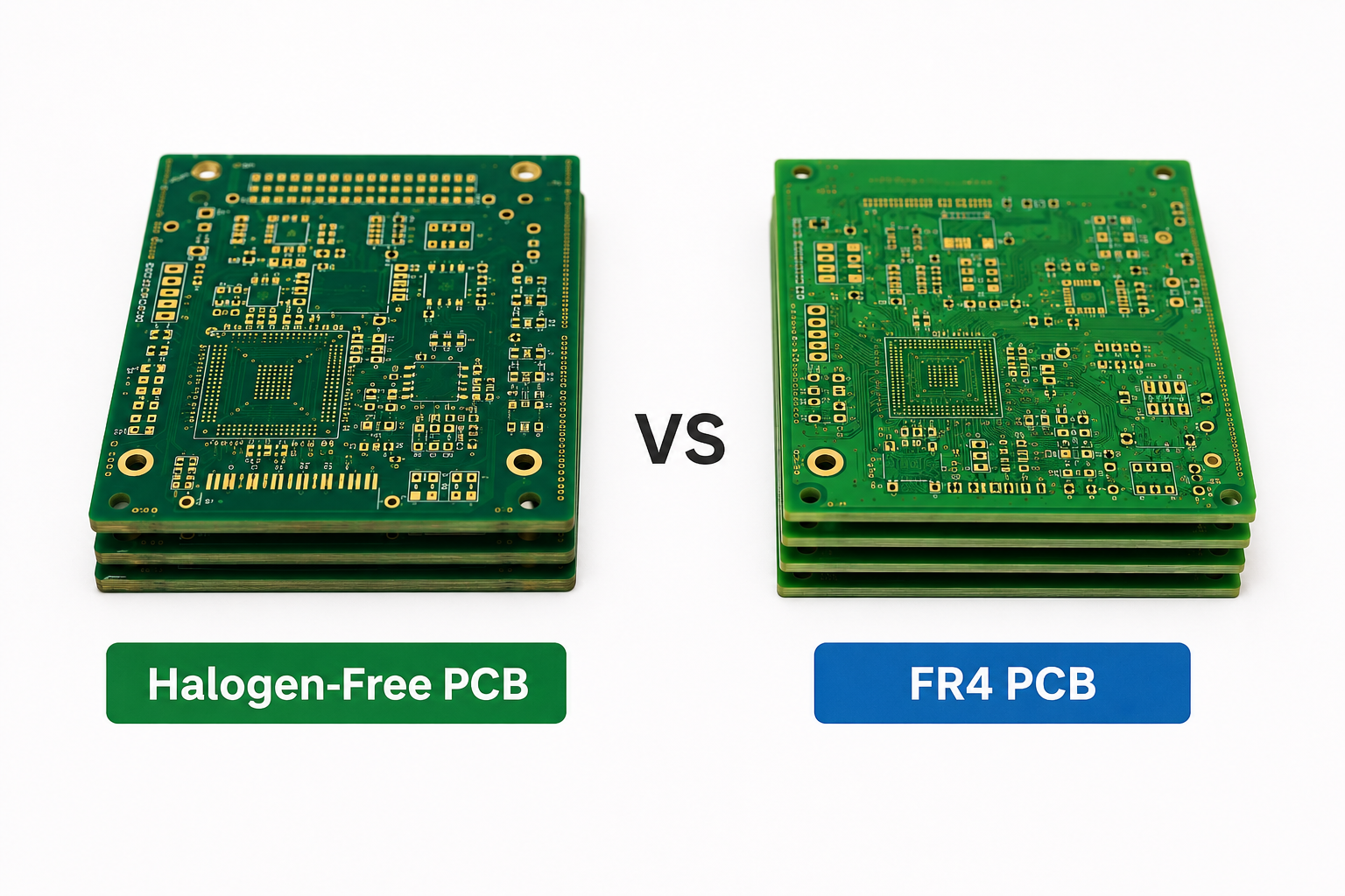
Yes. FR4 describes a flame-retardant glass-reinforced epoxy material class, while individual grades can use different flame-retardant systems. The exact laminate grade and its documentation determine whether it meets the project’s halogen-free requirement.
Should solder mask be included in the requirement?
Include solder mask when the customer specification applies to the finished bare PCB rather than only the base laminate. The same logic applies to legend ink, via-fill resin, bonding films, adhesives, and other materials that remain in the delivered board.
Is halide-free flux the same as halogen-free assembly material?
No. Halide-free classifications focus on ionic halides in flux chemistry, while a halogen-free product requirement may cover a broader set of halogen-containing compounds. Confirm the applicable assembly-material standard and customer definition before approving solder paste or flux.
When is third-party testing needed?
Third-party testing may be appropriate for first-article qualification, regulated or safety-sensitive products, disputed material identity, supplier changes, or contracts that explicitly require measured data. Routine lots may rely on approved material control and declarations when the customer specification allows it.
What sample should be tested?
The test specimen must match the scope of the requirement. A laminate coupon can support a base-material claim, but it may not represent solder mask, ink, adhesives, or assembly materials. Define whether the laboratory receives raw laminate, a finished bare board, or a complete assembly.
What changes require requalification?
Requalification may be required after a laminate or prepreg substitution, resin-system change, solder-mask change, manufacturing-site change, or customer drawing revision. The purchase agreement should identify which changes require notification, documentation review, or repeat testing.
Do halogen-free materials always cost more?
Not always, but approved-grade availability, special prepreg styles, minimum purchase quantities, lot testing, documentation, and restricted substitution can increase cost. Compare the complete stackup and compliance package rather than judging only the laminate unit price.
How Can EBest Circuit Support a Halogen-Free PCB Project?
At EBest Circuit, we review the fabrication drawing, stackup, approved material grade, assembly profile, and required compliance documents before quotation and production. Halogen-free FR4 is available as an optional material route, subject to the selected grade and project requirements.
Send us your Gerber files, stackup, quantity, approved material list, and compliance notes for review. Our team can clarify material availability, documentation scope, and manufacturability before the order is released. Contact us through our PCB enquiry page or email sales@bestpcbs.com.