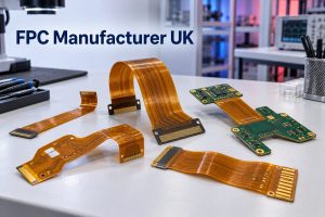
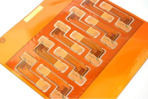
A flexible pcb board is a printed circuit built on a bendable dielectric film, usually polyimide, instead of a rigid laminate. It can replace wires and connectors, route signals through tight three-dimensional spaces, and move with a product. Reliable results depend on treating the bend requirement, material stack, copper construction, thickness and component locations as one system.
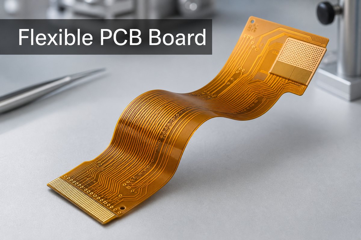
The first design question is not simply whether the circuit can bend. The team must define whether it bends only during installation or moves throughout the product’s service life. That distinction changes the stackup, copper choice, trace routing, bend radius, reinforcement and qualification plan.
What Is a Flexible PCB Board and When Should You Use One?
A flexible printed circuit board (PCB), also called an FPC or flex circuit, carries etched conductors on a thin flexible substrate. Use one when a conventional rigid board plus cable assembly creates too much volume, weight, assembly work or interconnection risk.
A flex circuit is especially useful when it must:
- fit around a housing, hinge, camera module, battery or other mechanical feature;
- replace point-to-point wiring with a repeatable conductor pattern;
- connect rigid sections without a separate cable and connector pair;
- reduce package thickness or weight; or
- survive controlled motion when the stackup is designed for dynamic flexing.
Pure flex is not automatically the best choice for every compact assembly. If components need a mechanically stable mounting area and the flexible interconnect must be permanently integrated with that area, a rigid-flex PCB may reduce connectors and assembly steps. If the circuit only needs to bridge two existing boards, a cable or flex jumper may be simpler to service.
Which Flexible PCB Board Materials Shape Performance?
The flexible pcb board material system controls electrical insulation, bend behavior, temperature exposure, dimensional stability and manufacturing yield. A useful material review looks beyond the base film and includes the conductor, bonding system, coverlay, stiffeners, shielding and exposed-pad finish.
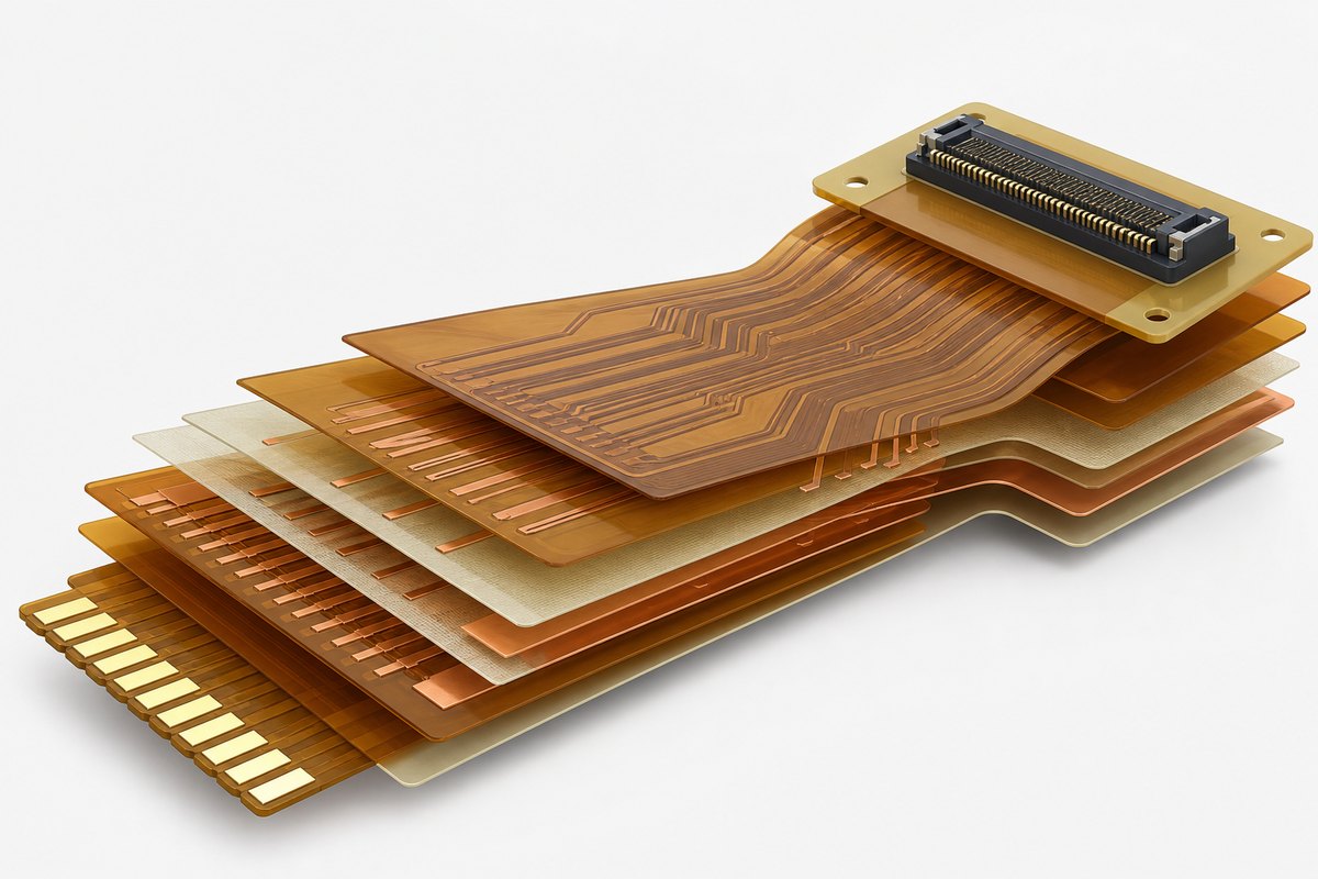
| Material element | What it does | Selection question |
| Polyimide film | Provides the flexible dielectric foundation and electrical insulation. | What temperature, dimensional stability and bend-life conditions must the circuit withstand? |
| Rolled-annealed or electrodeposited copper | Forms the conductors; copper grain structure and thickness influence flex fatigue and etching behavior. | Is the application static, installation-flex or dynamic-flex, and what current and fine-line needs apply? |
| Adhesive or adhesiveless construction | Bonds copper and dielectric layers or removes a separate adhesive layer from the core construction. | Is lower thickness, tighter bending or repeated movement more important than the economics of a conventional construction? |
| Coverlay | Protects conductors while leaving pads and contact areas exposed. | Can the coverlay opening and adhesive flow be controlled around fine-pitch pads and bend transitions? |
| Stiffener | Reinforces a connector, component or contact area without making the entire circuit rigid. | Where must insertion force, component support or finished thickness be controlled? |
| Shielding layer | Supports EMI control and reference continuity but adds thickness and can reduce flexibility. | Does the electrical need justify the mechanical and cost trade-off? |
Material names alone do not define performance. The copper weight, adhesive thickness, coverlay construction, plated features and local reinforcement all change the finished stack. For a deeper material review, see the BestPCBs guide to flexible PCB materials.
Which Flexible PCB Types Fit Different Layer and Bend Needs?
The main flexible pcb types are single-sided, double-sided and multilayer flex circuits, plus rigid-flex constructions that combine rigid and flexible sections. Choose the simplest structure that meets routing, shielding, current, connector and mechanical needs because every added layer increases thickness and makes the bend region harder to manage.
| Type | Best fit | Main design watchpoint |
| Single-sided flex | Simple jumpers, sensors, membrane interfaces and low-density interconnects. | Limited routing and no plated connection between conductor sides. |
| Double-sided flex | More routing density, plated-through connections and circuits needing conductors on both sides. | Added copper and plating make the stack less compliant than a single-sided circuit. |
| Multilayer flex | Dense signal routing, shielding, controlled references or complex interconnection. | Layer count, bonded areas and via placement must be coordinated with the intended bend zones. |
| Rigid-flex PCB | Assemblies that need component-bearing rigid areas connected by integrated flexible sections. | The rigid-to-flex transition, layer construction and fabrication sequence require early supplier review. |
Do not select a layer count from routing density alone. First identify the active bend area, then check whether reference planes, shielding, plated holes or bonded multilayer sections can stay outside it. A thinner, simpler flex tail connected to a rigid component area may be more reliable than forcing every electrical feature through a moving zone.
Flexible PCB Design Rules for Reliable Bending
Reliable flexible pcb design keeps mechanical strain low and avoids local stress concentrations. The bend region should be treated as a controlled mechanical feature, not as leftover routing space after the electrical layout is complete.
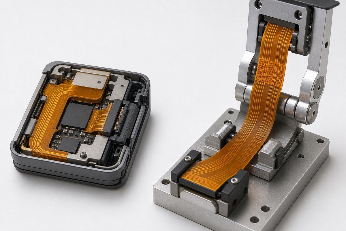
- Define the motion: record whether the bend occurs once during assembly, occasionally during service or continuously through many cycles.
- Route traces through the bend: use smooth, consistent paths and avoid abrupt width changes, sharp corners and unnecessary jogs in high-strain areas.
- Keep discontinuities away: move vias, plated holes, component pads and stiffener edges out of the active bend wherever the design permits.
- Stagger features: avoid creating a straight line of vias or pad edges that concentrates strain across the circuit width.
- Manage copper direction: align conductor paths with the intended bending action and review plane or hatch patterns for both electrical and mechanical behavior.
- Use gradual transitions: add suitable fillets, teardrops or other strain-relief geometry where conductors enter pads, subject to fabricator DFM rules.
- Control the installed shape: prevent folds, pinching, torsion and contact with sharp housing edges.
Static and dynamic flex should not share an unexamined rule set. A circuit bent once and retained in a housing can often use a different stack and routing approach from a circuit moving in a hinge. Review bend direction, bend angle, available envelope, motion cycles and environmental conditions with the manufacturer before freezing the mechanical design.
How Do Flexible PCB Thickness, Bend Radius and Stiffeners Work Together?
Flexible pcb thickness and bend radius are linked: a thicker, more heavily bonded stack generally develops more strain for the same bend geometry. Stiffeners solve local support problems, but their edges also create transitions that must be kept away from active bending.
There is no single bend-radius multiplier that is safe for every flex circuit. The required radius depends on:
- single-sided, double-sided or multilayer construction;
- finished thickness and local thickness changes;
- copper type, copper thickness and plating;
- adhesive-based or adhesiveless materials;
- static installation versus repeated dynamic movement;
- trace orientation and density inside the bend;
- coverlay, shielding and reinforcement; and
- temperature, assembly constraints and expected service life.
Use IPC-2223 as a design reference, then obtain a stack-specific DFM review instead of treating one online ratio as a universal guarantee. The BestPCBs overview of IPC-2223 and flex PCB bend radius explains why construction and use conditions must accompany any bend recommendation.
What Are the Advantages and Disadvantages of a Flexible PCB?
A flex circuit can reduce interconnect volume, weight and assembly complexity, but it demands closer coordination between electrical, mechanical and manufacturing decisions. Its value should be judged at the assembly level, not by bare-board price alone.
| Potential advantage | Corresponding limitation |
| Routes through compact three-dimensional spaces. | The installed bend and housing clearances must be controlled. |
| Can replace wires and connector interfaces. | Design changes may require a new artwork, tooling or mechanical review. |
| Supports low-profile, lightweight assemblies. | Thin circuits need suitable handling, fixtures and support during assembly. |
| Provides repeatable conductor routing. | Poor bend-zone layout can create concentrated copper fatigue. |
| Can move with hinges or mechanisms when designed for dynamic use. | Dynamic life depends on the complete material stack, geometry and motion profile. |
| May simplify final assembly and reduce interconnection count. | Bare flex fabrication can cost more than a comparable simple rigid board. |
A design that saves two connectors, a cable and manual routing time may reduce total installed cost even when the flex circuit itself has a higher unit price. Conversely, a simple stationary product with generous space may gain little from flexible construction.
What Drives Flexible PCB Board Price and Supplier Selection?
Flexible pcb board price is driven by the stackup, panel utilization, feature density, reinforcement, surface finish, testing and production volume. A useful quote therefore needs more than Gerber files and a layer count.
Common cost and manufacturability drivers include:
- board outline, nesting efficiency and array or panel requirements;
- material family, adhesiveless construction, copper type and copper thickness;
- layer count, finished thickness and selective bonding requirements;
- minimum trace, spacing, annular ring and hole features;
- coverlay openings, fine-pitch pads and adhesive-flow control;
- stiffeners, shielding films, pressure-sensitive adhesive and local reinforcement;
- surface finish, impedance requirements and electrical testing;
- prototype versus production quantity and repeat-order expectations; and
- assembly fixtures, component loading and final functional tests when PCBA is included.

When comparing flexible pcb board manufacturers, ask each supplier to review the same controlled data package. Include fabrication files, drawing, stackup, material requirements, finished thickness, stiffener details, bend location, bend direction, minimum installed radius, expected motion cycles, surface finish, test requirements, quantities and assembly scope. This makes quotations more comparable and exposes DFM assumptions before they become production changes.
For a manufacturing-focused evaluation path, review BestPCBs’ flex PCB manufacturer page, then request written confirmation for the exact stackup and mechanical use case rather than relying on a generic capability statement.
Flexible PCB Board RFQ Checklist
A complete RFQ should define the mechanical life of the circuit as clearly as its electrical construction. The following inputs reduce avoidable assumptions during DFM and quotation.
- Gerber or ODB++ fabrication data, drill files, netlist and a controlled drawing.
- Layer stack, copper requirements, base film, coverlay and any adhesive restrictions.
- Finished thickness, thickness tolerance and local stiffener thickness.
- Bend-zone drawing with bend direction, angle, available radius and installed envelope.
- Static, installation-flex or dynamic-flex classification, including expected cycles for moving designs.
- Connector, contact-finger, component and assembly requirements.
- Surface finish, impedance, shielding, pressure-sensitive adhesive and marking requirements.
- Electrical test, dimensional inspection, reliability or functional-test requirements.
- Prototype quantity, production volumes, panel preferences and delivery destination.
Mark critical dimensions and bend restrictions on the drawing rather than leaving them in an email thread. If the supplier proposes a material or stack change, request an updated stackup and confirm its effect on thickness, impedance, bending and assembly interfaces before approval.
Frequently Asked Questions
Is a flex board the same as an FPC?
In most PCB manufacturing contexts, flex board, flexible circuit and FPC refer to the same product family: patterned conductors supported by a flexible dielectric. Individual suppliers may use the terms differently for product categories, so the fabrication drawing and stackup should define the construction instead of relying on the label alone.
Can a flexible PCB be bent repeatedly?
Yes, but only when it is designed for dynamic flexing. Repeated motion requires a compatible material stack, suitable copper, controlled thickness, smooth trace routing, an adequate bend radius and a defined motion path. A circuit designed only for installation flex should not be assumed to survive continuous hinge movement.
How many layers can a flexible PCB have?
Flexible circuits can be single-sided, double-sided or multilayer. The practical layer count depends on the fabricator, material set, routing density and whether the area must bend. More layers increase thickness and strain, so designers often keep active bend zones simpler than component or termination areas.
Why can a flexible PCB cost more than a rigid PCB?
Flex fabrication uses specialized films, coverlay processing, handling, reinforcement and inspection. Complex outlines and low panel utilization can also affect price. The relevant comparison is total assembly cost: a flex circuit may remove cables, connectors and manual wiring even when its bare-board price is higher.
Can components be mounted directly on a flexible PCB?
Yes. Component areas normally need suitable support, land patterns, assembly fixtures and strain control. Stiffeners are often used beneath connectors or component regions, while active bending is kept away from solder joints and abrupt stiffener edges.
Which surface finishes can be used on flexible PCB pads?
Several common PCB finishes can be applied, but the correct choice depends on pad function, soldering, contact wear, storage, assembly process and supplier capability. Connector fingers and solderable component pads may have different requirements, so define each finish area on the fabrication drawing.
Can controlled impedance be designed on a flex circuit?
Yes. Impedance control requires defined dielectric thickness, copper geometry, reference structure and material properties. Bending and stack transitions can affect geometry, so controlled-impedance regions and moving zones should be reviewed together with the fabricator.
Should vias be placed in a bend area?
Vias are stress discontinuities and should generally be kept outside an active bend when the layout allows. If packaging makes that impossible, the via construction, reinforcement, bend direction and use condition need an explicit DFM and reliability review.
Can a damaged flexible PCB be repaired?
Some pad, trace or component-area defects may be repairable under a controlled procedure, but damage in a repeatedly flexing region is difficult to restore reliably. Repair feasibility depends on access, conductor geometry, insulation restoration and the product’s reliability requirements.
What files are needed for a flexible PCB quote?
Provide fabrication data, drill files, a controlled drawing, stackup, material and thickness requirements, stiffener details, bend-zone geometry, motion classification, finish, testing needs and quantities. For assembly, also include the BOM, centroid data, assembly drawings and any programming or functional-test instructions.
Plan the Stackup Around the Bend Requirement
A dependable flex circuit starts with a defined mechanical use case. Establish the bend zone and motion profile first, then select materials, copper, layer count, thickness, stiffeners and routing that support that requirement. Complete drawings and early DFM review are more valuable than applying a generic bend rule after layout.
If you need a flex PCB fabrication or assembly review, send the BestPCBs engineering team your files, stackup, quantities, bend radius and motion-cycle requirements at sales@bestpcbs.com. The team can review manufacturability and prepare a project-specific quotation.