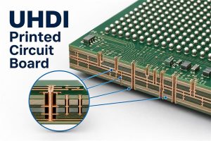
The emc meaning in electronics is electromagnetic compatibility: the ability of equipment to work as intended in its electromagnetic environment without creating unacceptable interference for other equipment. In practical terms, an EMC-compatible product controls what it emits and continues operating when exposed to expected disturbances.
EMC is a system-level result, not a single component or PCB feature. Circuit architecture, PCB stackup, return paths, power integrity, cables, shielding, enclosure design, firmware states, and the test setup can all change the result. Engineers therefore need to address EMC during design and verify it against the standards that apply to the finished product.
Key Takeaways
- EMC stands for electromagnetic compatibility, the ability of electronic equipment to operate correctly without causing or suffering unacceptable electromagnetic interference.
- The purpose of EMC is to let electronic devices coexist reliably by limiting emissions and maintaining immunity in their intended electromagnetic environment.
- EMC testing checks both emissions and immunity under the standards, operating modes, cable arrangements, and performance criteria applicable to the finished product.
- In the United States, EMC requirements depend on the product and its functions, so the applicable FCC rules and product standards must be confirmed for each device.
- EMI risk can be reduced through continuous return paths, compact switching loops, correct decoupling, connector filtering, cable control, shielding, and appropriate enclosure design.
- EMI and EMC are not interchangeable terms, because EMI is the unwanted electromagnetic disturbance while EMC is the broader goal of controlling emissions and maintaining immunity.
What Does EMC Mean in Electronics?
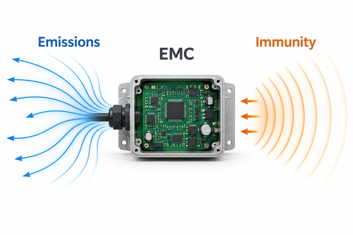
In electronics, EMC means that a device can coexist with other electrical and electronic equipment in its intended environment. The device must keep its electromagnetic emissions within the applicable limits and maintain acceptable operation when exposed to defined disturbances.
This definition has two complementary sides:
- Emissions: electromagnetic energy leaving the product through radiation or conductors must remain below the applicable limits.
- Immunity: the product must continue to meet specified performance criteria when exposed to disturbances such as RF fields, electrostatic discharge, transients, or conducted noise.
The phrase emc meaning in electronics is sometimes reduced to “no interference,” but that is incomplete. Every operating circuit produces electromagnetic energy. EMC engineering controls that energy and its coupling paths so nearby systems can operate together.
What Is the Difference Between EMC, EMI and EMS?
EMC is the ability to coexist, EMI is the disturbance that causes or may cause a problem, and EMS describes susceptibility to that disturbance. The terms are related, but they are not interchangeable.
| Term | Full Form | Practical Meaning |
| EMC | Electromagnetic compatibility | The product limits emissions and tolerates specified disturbances in its intended environment. |
| EMI | Electromagnetic interference | Unwanted electromagnetic energy that can degrade or disrupt operation. |
| EMS | Electromagnetic susceptibility | The tendency of equipment to be affected by electromagnetic disturbances; immunity expresses resistance to them. |
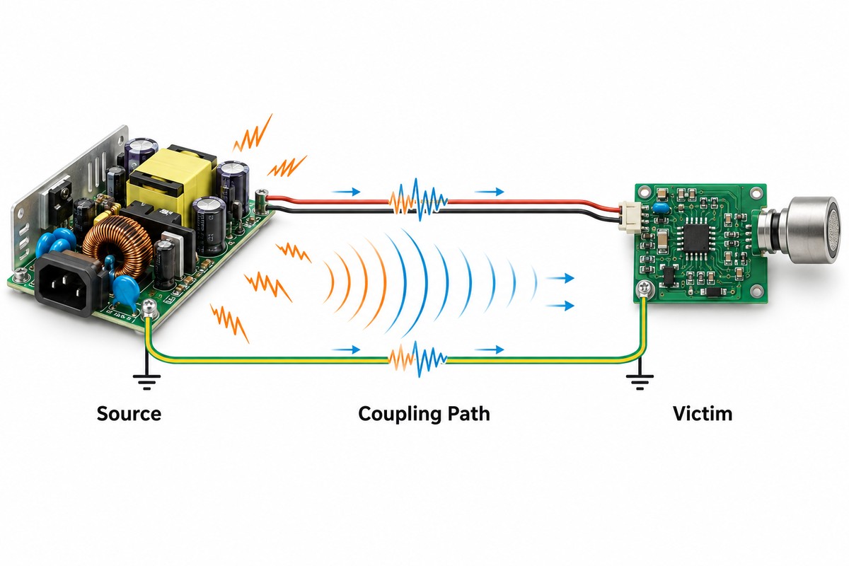
For example, a switching converter can be an EMI source, a cable can provide a coupling path, and a sensitive analog input can be the victim. An EMC design review looks at the complete source-path-victim relationship rather than treating the noise source alone.
What Does EMC Cover: Emissions, Immunity and Coupling?
EMC covers how disturbances are generated, how they travel, and how circuits respond. A useful diagnosis separates the source, coupling path, and victim because changing any one of the three can reduce the problem.
- Conducted coupling: noise travels through power, ground, signal, or cable conductors.
- Capacitive coupling: changing electric fields transfer energy between nearby conductors.
- Inductive coupling: changing magnetic fields induce voltage in an adjacent current loop.
- Radiated coupling: traces, cables, slots, or enclosures behave as transmitting or receiving structures.
Fast edge rates often matter more than the nominal clock frequency. A low-frequency digital signal with sharp transitions can contain high-frequency energy, while a cable connected to the board can convert common-mode current into radiated emissions.
What Is EMC Testing?
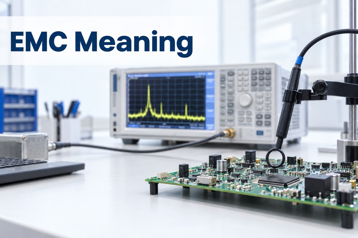
The emc testing meaning is the controlled evaluation of a product’s emissions and immunity against specified limits, test levels, setups, and performance criteria. It is not one universal test; the correct program depends on the product category, intended environment, interfaces, power source, and target market.
If you are asking what is emc testing, the most useful distinction is between pre-compliance and formal compliance work. Pre-compliance measurements help find high-risk frequencies, cables, operating modes, and PCB areas before the final test. Formal testing follows the applicable standard using the required equipment, calibrated setup, distances, limits, and documentation.
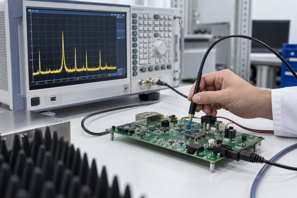
For a deeper test-oriented overview, see our guide to EMI and EMC testing in PCBs.
Which EMC Tests Are Common for Electronic Products?
Common EMC evaluations include conducted and radiated emissions plus several immunity tests, but not every product needs every test. The applicable product or product-family standard should define the final test plan.
| Test | What It Evaluates | Typical Coupling Path |
| Conducted emissions | Noise returned through power or connected conductors | Power leads and cables |
| Radiated emissions | Electromagnetic energy radiated by the product and its cables | Enclosure openings, traces, cables, and common-mode currents |
| Radiated RF immunity | Operation under an external radio-frequency field | Enclosure, PCB, and cables acting as receiving structures |
| Conducted RF immunity | Response to RF energy coupled onto connected cables | Power and signal ports |
| Electrostatic discharge | Response to direct or indirect ESD events | Exposed metal, seams, displays, buttons, and connectors |
| EFT/burst and surge | Response to fast repetitive transients or higher-energy events | Power and external I/O wiring |
Performance criteria also matter. A disturbance may permit no degradation, temporary self-recovery, or controlled operator intervention depending on the applicable standard. Teams should define acceptable behavior before the test instead of deciding after a failure.
Why Do PCBs Cause EMC Problems?
PCBs contribute to EMC problems when fast currents flow through large or discontinuous loops, when noise couples into sensitive nodes, or when common-mode energy reaches an efficient radiator such as a cable. The schematic may be correct while the physical current paths are not.
Frequent board-level causes include:
- high-speed traces crossing a split or void in the reference plane;
- large switching-current loops around converters, drivers, or power devices;
- decoupling capacitors placed too far from IC power and ground pins;
- long parallel routes that increase crosstalk;
- filters placed far from the connector where interference enters or leaves;
- poor shield or chassis termination that forces high-frequency current through signal ground;
- layer changes without a nearby return-path transition;
- uncontrolled cable common-mode current.
A PCB is only one part of the final electromagnetic structure. The enclosure, harness, display, power supply, grounding arrangement, connector shells, and installed accessories can turn a small board-level noise source into a compliance failure.
How Can PCB Layout Improve EMC Performance?
PCB layout improves EMC by reducing loop area, preserving continuous return paths, containing high-frequency fields, and preventing noise from reaching external cables. The most effective changes are usually architectural and placement-related, not late additions of random filter components.
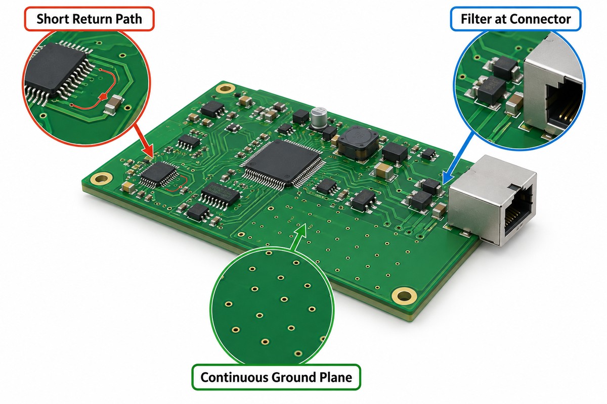
- Route critical signals over a continuous reference plane and avoid plane splits beneath them.
- Keep switching loops compact and place high-di/dt components close together.
- Place decoupling capacitors at the relevant power pins with short connections to the reference plane.
- Keep noisy power sections away from clocks, RF paths, analog inputs, and external connectors.
- Place filtering and transient protection at the connector boundary.
- Provide nearby stitching vias when signals change reference layers.
- Control impedance, return paths, and pair geometry for fast interfaces.
- Plan shield-can pads, via fences, chassis bonds, and keep-outs before routing is complete.
Our article on the circuit board ground plane explains why return-path continuity and layer references are central to both signal integrity and EMC.
Which Standards and Regulations Apply to EMC?
The applicable EMC requirements depend on the product, environment, interfaces, and market. There is no single “EMC certificate” or universal test list that covers every electronic device.
Common frameworks include the IEC 61000 series for EMC terminology and test methods, CISPR publications for many emissions requirements, FCC rules for relevant radio-frequency emissions in the United States, and the EU EMC Directive for equipment placed on the European market. Product-specific families can add different limits, ports, test levels, operating modes, and performance criteria.
Examples include IEC 61326-1 for certain measurement, control, and laboratory equipment and IEC 60601-1-2 for medical electrical equipment. These examples should not be treated as automatic selections. Confirm the product classification and current edition with the compliance laboratory or responsible regulatory specialist before freezing the test plan.
How Should You Prepare an EMC-Sensitive PCB for Manufacturing?
An EMC-sensitive board should be released with the stackup, reference planes, controlled-impedance requirements, grounding details, shield features, connector interfaces, and assembly notes clearly defined. Fabrication and assembly must preserve the electrical geometry on which the design depends.
Before sending the package, check that it includes:
- Gerber, ODB++, or IPC-2581 data plus drill and route files;
- a stackup drawing with materials, finished thickness, and copper requirements;
- controlled-impedance definitions and coupon requirements where applicable;
- a released BOM with filter, protection, and shielding components identified;
- pick-and-place and assembly drawings with polarity and shield orientation;
- notes for via filling, ground stitching, shield-can pads, and connector-shell grounding;
- inspection and electrical-test requirements appropriate to the build.
An EMC test is still performed on the finished product or representative system, not on bare Gerber data alone. Manufacturing documentation reduces unintended variation, but it does not replace system-level compliance validation.
FAQ About EMC Meaning
What does EMC stand for in electronics?
EMC stands for electromagnetic compatibility. It describes whether electronic equipment can operate satisfactorily in its intended electromagnetic environment without causing unacceptable interference to other equipment.
Does EMC mean a device produces no EMI?
No. Every active electronic product produces some electromagnetic energy. EMC means emissions remain within the applicable limits and the product has the required immunity for its intended environment.
Is EMC the same as FCC or CE compliance?
No. EMC is the engineering and performance concept. FCC requirements, the EU EMC Directive, and product standards are regulatory or conformity frameworks that may define specific emissions, immunity, documentation, and assessment obligations.
Can a PCB manufacturer certify the finished product’s EMC?
A PCB manufacturer can build the specified stackup, impedance, grounding, shielding pads, and assembly features. Formal product compliance normally requires testing the representative finished equipment under the applicable standard and configuration.
Does a solid ground plane guarantee good EMC?
No. A continuous reference plane usually improves return-path control, but poor connector grounding, large switching loops, cable common-mode current, enclosure seams, or unsuitable filtering can still cause emissions or immunity failures.
Why can a prototype pass while a later version fails?
Changes to the stackup, component substitutions, cable routing, enclosure bonding, firmware modes, clock edges, power supply, or test configuration can change EMC behavior. Revision control should include both electrical design files and the representative test setup.
Is pre-compliance EMC testing worthwhile?
Yes. Near-field scanning and other pre-compliance checks can identify dominant frequencies, noisy PCB regions, cable effects, and operating modes before formal testing. They reduce risk, but they do not replace the required compliance test.
How Can EBest Circuit Support an EMC-Aware PCB Build?
EMC performance begins with system design, while consistent PCB fabrication and assembly help preserve the intended stackup, return paths, impedance geometry, grounding features, and shielding interfaces. At EBest Circuit, we support PCB fabrication and PCBA from prototype through volume production using the released manufacturing data and agreed inspection scope.
For projects involving industrial interfaces, power conversion, fast digital links, or shielded connectors, our industrial network PCB design checks provide a useful release reference. Send your Gerber files, stackup, BOM, assembly data, quantities, and EMC-related manufacturing notes to sales@bestpcbs.com for engineering review and a quotation.