PCB manufacturing PCB manufacturing
Home > Blog

board level emi shielding

EMI Shielding Failures in Small Medical Devices
Friday, November 13th, 2026
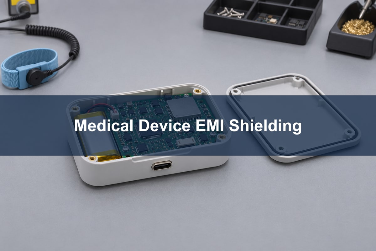
Open handheld instrument enclosure with a PCB and metal shield lid
Illustrative rendering; not a tested medical device or measurement record.

When EMI shielding fails in a compact medical device, first determine whether the disturbance bypasses the shield through a cable, leaks through a seam or enters the sensitive circuit by another path. A larger metal cover will not fix every mechanism. Compare one controlled change at a time and verify both the electromagnetic result and the device function.

Consider a hypothetical handheld monitor that behaves normally on its bench supply but occasionally produces a sensor error during immunity evaluation with its intended cable attached. The goal is to localize the coupling path, decide what to change and confirm the fix on the assembled device. This example is not a compliance procedure or a record of a tested product.

Board level shielding

Use a board shield to enclose a defined source or protect a defined victim. The can, its connection to the board reference and the return path underneath form one enclosure. A shield that covers a regulator while leaving the connector return outside the boundary may reduce a local field without changing the disturbance that reaches the sensor.

Mark three features on the layout: the suspected source, the sensitive circuit and each conductor crossing the shield boundary. Include flex tails and test leads. If the error occurs only with the external cable attached, investigate that path before changing the can. If a local source couples directly into the analog input, inspect where those circuits share geometry or return impedance.

PCB shield can

Choose a one-piece can or a removable lid according to the required RF continuity, assembly process and service access. A two-piece part can simplify inspection and rework, but the lid-to-frame interface becomes a separate contact to verify. A one-piece part still depends on how it is attached and on what passes underneath it.

Option Use when Verify on the build
One-piece board shield The region does not need routine access. Attachment, coplanarity and inspection of required joints.
Frame with removable lid Parts must remain accessible during build or service. Lid seating and repeatability after approved reassembly.
Conductive enclosure and gasket The coupling path crosses a case seam or port. Mating surfaces, contact continuity and the approved boundary design.

Use the chosen part’s drawing for footprint, flatness and height. After assembly, check that the lid does not contact tall components and that it seats with the actual board thickness and enclosure tolerances. Do not rely on a supplier shielding figure for the behavior of an assembled medical device.
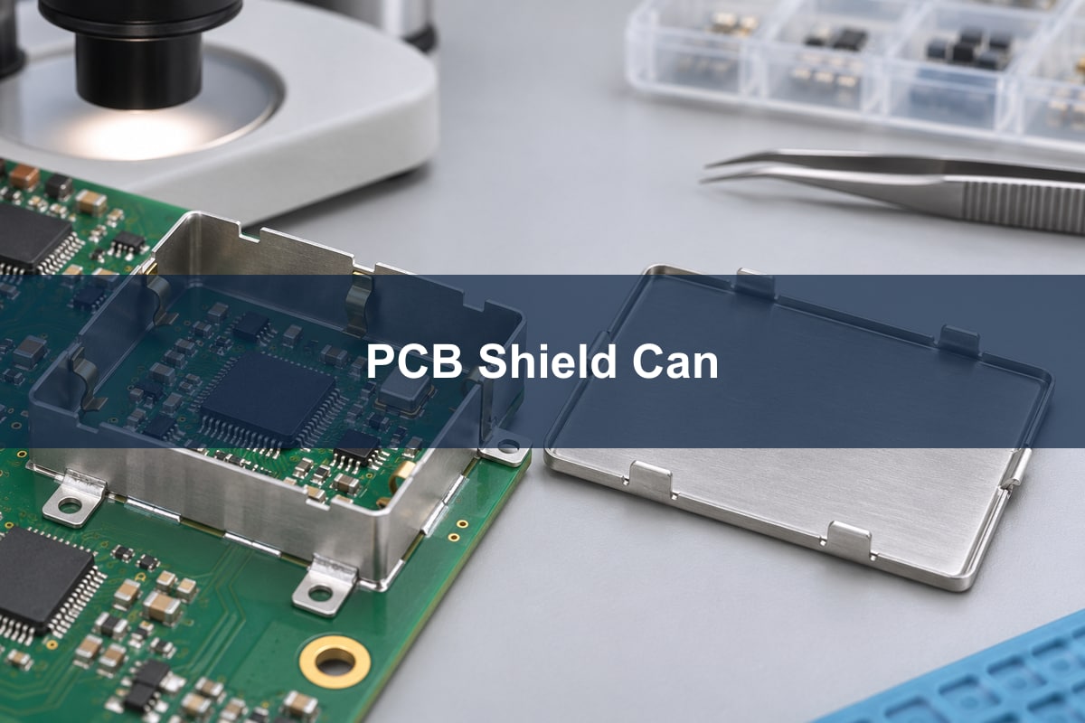
Removable metal shield beside its PCB mounting frame
Illustrative rendering; not a tested medical device or measurement record.

EMI gasket

A conductive gasket is useful only when it provides a repeatable contact across the seam it is intended to close. Inspect the actual mating surfaces for paint, gaps, pressure variation and housing distortion. A gasket that touches at the screws but loses contact between them can leave an RF leakage path even if a continuity meter beeps.

On the monitor, compare the baseline with a reversible engineering change applied to one suspected seam. Keep cable position and operating mode unchanged. Use only changes approved for the test unit: a diagnostic bond must not bypass patient isolation, protective barriers or other safety features. If the improvement depends on hand pressure, treat that as a clue about contact repeatability rather than a production fix.

Common mode current

Look for cable common-mode current when a change in cable orientation, accessory or connector bond shifts the response more than a change to the can. A clamp around all conductors in a cable can help compare net current under repeatable conditions. The measurement is a diagnostic proxy; it does not by itself establish how much of the disturbance reaches a sensitive node.

Compare only configurations allowed by the test plan. For the example monitor, log whether the cable is attached, its routing and termination, and the operating mode. If the error follows a cable change, examine the port protection and return path. Do not copy a chassis-bonding recommendation from another product where it could change leakage current or isolation.

Near field probes

Use a probe to compare local RF activity at the shield edge, connector and nearby circuits. Keep probe orientation, distance and analyzer settings fixed. When the lid is installed, the geometry changes; use the same accessible comparison points and do not compare readings taken at different distances as if they were equivalent.

A quieter regulator region with no change at the cable entry suggests that the local shield changed one path but not necessarily the one responsible for the error. Check the cable-current trend and the device log under the same conditions. The near-field probe troubleshooting guide explains the bench comparison in more detail.

Shielding effectiveness measurement

State what was compared before reporting a shielding change in decibels. A material coupon, local probe and full assembly test measure different quantities. A local result can guide a design change but cannot be transferred directly to the installed device or to a different frequency band.

Observation Likely next check What it does not prove
Local peak drops after lid installation. Check cable behavior and device response. That the final product meets emissions or immunity criteria.
Error changes with documented cable movement. Investigate the connector and common-mode path. That the shield lid is defective.
Result changes when the seam is pressed. Check lid seating, gasket pressure and repeatability. That an operator-dependent improvement is suitable for production.

For example, a receiver reading that changes from 55 to 47 dB”V in an unchanged bench setup shows an 8 dB drop for that observation. These are hypothetical readings. Do not call the difference enclosure shielding effectiveness unless the measurement method and geometry support that claim.

EMC immunity testing

Judge immunity by how the device performs under the specified disturbance, not by how quiet its spectrum looks. Log the observable product function, disturbance and configuration together. A lower local RF reading does not prove that a sensor reading, alarm or recovery behavior stays within its approved criterion.

For the hypothetical monitor, engineering should identify the sensor error or degradation that matters, how it is logged and how normal operation is assessed after exposure. The qualified product team defines the acceptance criteria from the intended use and applicable requirements. The FDA’s EMC guidance discusses device functions, intended environments, accessories and test evidence; it does not provide a universal shield design.

EMC test plan

Freeze the released assembly and record exactly what is being verified. Include the board revision, shield and gasket parts, housing, harness, supported accessories, operating modes and approved criteria. Before the formal evaluation, repeat the baseline and the proposed change in representative configurations so a result can be traced to the actual design difference.

In the example, release the fix only after the error is absent under the agreed conditions, the change is repeatable across the planned units and assemblies, and applicable safety and performance checks remain satisfied. If the result depends on one prototype, one cable position or one lid, keep the investigation open. Formal evaluation belongs with the product team and qualified lab.

FAQ

Why can a board pass emissions but fail immunity?

Emissions and immunity ask different questions: what the device produces and how it behaves when disturbed. A shield or filter may improve one path without protecting every affected function.

Does DC continuity prove good shielding?

No. It can reveal an open bond, but it does not characterize RF impedance around the whole seam or connector. Check contact geometry and compare performance under repeatable conditions.

Can removing a shield reduce one measured peak?

Yes. Changing the cover can change coupling, resonance or current paths. Compare the complete band and required operating configurations before accepting the result.

Why does a replacement lid need its own review?

Contact geometry, coatings and fit may change even if the outer dimensions match. Compare the drawing and the assembled contact condition, then repeat the affected verification.

Should the device always be tested while charging?

Include charging or other connected modes when they are part of intended use and the applicable plan. Keep the charger and cable identification with the configuration record.

Can a clip-on ferrite prove the cable is the only problem?

No. An improvement indicates that modifying the cable path affected the outcome. Other paths can still be present. Retest the affected modes and confirm the production solution separately.

Does a shield require rechecking thermal behavior?

Consider it if the change affects ventilation, heat transfer or component clearance. Compare temperatures in the assembled unit under the specified operating conditions rather than assuming a metal cover always improves cooling.

What belongs in the supplier package?

Include the shield land pattern, part and revision, height envelope, assembly constraints and inspection points. Keep product-level immunity acceptance with the device verification plan.

References

Discuss shield and board integration

For a Best Technology fabrication or assembly review, send the PCB revision, shield drawing and inspection requirements to sales@bestpcbs.com. Keep the complete-device EMC verification plan with the product team.

You may also like

PCB EMI Simulation Software: Choose the Right Model
Friday, November 13th, 2026
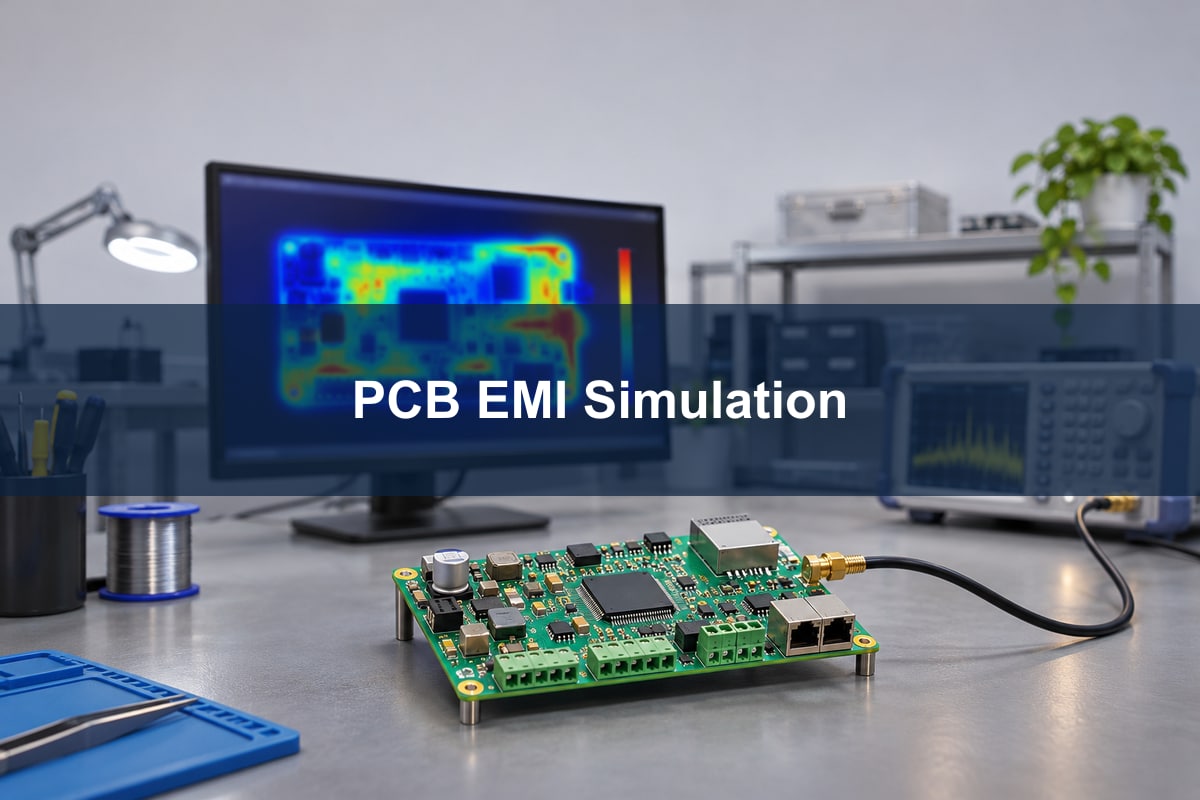
Controller PCB and cable next to a simulated field map on a laboratory monitor
Illustrative rendering; not a measurement or lab record.

Choose EMI simulation software by the decision you need to make. A circuit model can help explain which source drives a disturbance; a board field solver can show where current flows or couples; a system model can test whether a cable or enclosure changes radiation. None of these replaces an emissions test on the actual product.

Use this guide when a PCB design is still editable and you need to choose what to model before committing to another prototype. The running example is a hypothetical controller with a fast clock and an external coax connection. The question is whether to revise the board return path or investigate current on the outside of the cable shield first.

EMI simulation software

Start with the simplest model that includes the relevant source, coupling path and observation point. The useful output may be a port current, a relative field map or a predicted field at a specified location. Choose that output before picking a tool: an attractive field image is not a substitute for the quantity your decision requires.

Model type Decision it supports What it may miss
Circuit model Compare source spectra, termination and damping. Distributed geometry or radiation unless represented explicitly.
Board field solver Locate return-current detours and compare layout changes. Cables or chassis features omitted from the model.
3D assembly model Compare coupling through connectors, cable and enclosure. Operating modes or test arrangements not included in the model.

For the controller, first determine which clock harmonics need investigation. Ansys documents both board-level network extraction and near-field analysis in SIwave. These are distinct outputs, not interchangeable labels for an emissions prediction.

PCB EMI simulation

Define the source, return and measurable quantity in the same setup. Import the actual board revision and stack-up, then verify reference planes, plane cuts, vias and connector bonds. A model with a missing plane opening can be numerically stable and still represent a different board.

Set each excitation between the relevant conductors rather than connecting everything to a single ideal ground. Use a measured or documented source spectrum when amplitude matters. If a unit current is used to compare paths, label the result as a transfer comparison. It cannot be interpreted as the absolute noise generated by the operating controller.

PCB field solver

Use a board-focused solver for a predominantly planar path; use a 3D model when the return path runs through connector contacts, shielding or enclosure features not represented by the board model. Start with the suspected region and expand it when the result changes with the boundary or cutout.

For the controller, preserve the copper between the clock source and the connector, including the connector ground contacts and local return path. Compare the as-built board with a version where that return remains continuous. If the two cases give nearly the same connector current, don’t assume the detour is irrelevant; first check whether the excitation and the connector model are capable of revealing the difference.

Mesh convergence study

Refine the mesh until the quantity used for the decision stops changing materially between passes. A stable overall scattering-parameter result is helpful, but a local current at the connector can still be sensitive to how a narrow gap, via or port is modeled. Track the chosen observable as well as the solver’s convergence flag.

Suppose the project uses a 1 dB refinement tolerance for connector-current magnitude at a suspected harmonic. If successive passes change the magnitude by 0.4 dB but move the peak to a different part of the band, the model is not yet adequate for choosing a frequency-specific fix. The 1 dB is a teaching assumption, not a compliance limit. Recheck the sweep, refinement frequencies and port before proceeding.

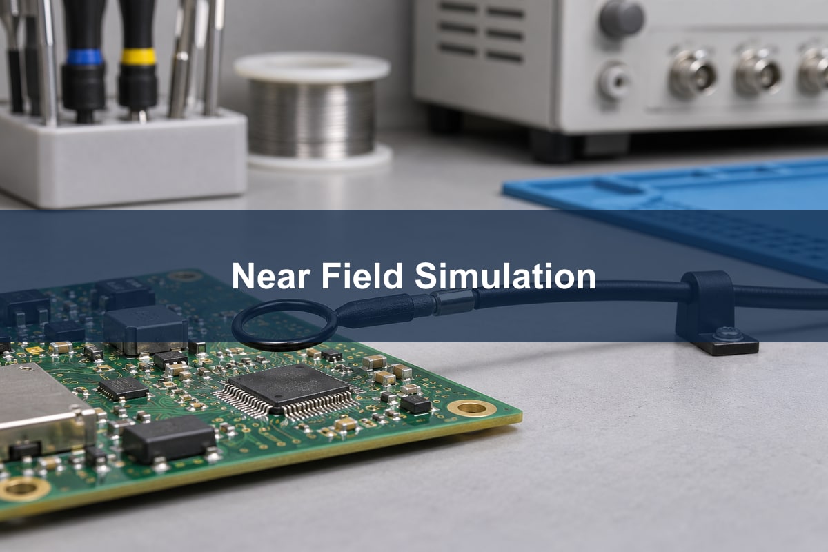
Magnetic loop probe held above a PCB on a lab bench
Illustrative rendering; not a measurement or lab record.

Near field simulation

Use near-field simulation to compare where energy is concentrated close to the board, not to infer a chamber reading. Record the field component, sampling plane, distance from the board and frequency. Compare maps using the same color scale; automatically normalized pictures can make two very different amplitudes look identical.

On the first prototype, use repeatable probe height, orientation and fixture position to look for the predicted hotspot. A magnetic loop responds to field components according to its orientation. A relative hotspot check is useful even when the instrument or model is not calibrated for absolute field strength. The near-field probe guide covers the bench technique in more detail.

Common mode current in coaxial cable

Current on the exterior of a coax shield can take a different return path from the intended center-conductor and inner-shield current. Include the connector bond and the external path when the predicted board hotspot does not explain why emissions change as the cable is moved.

Compare two controlled configurations: same board and operating mode, but different documented cable placement or shield bond. Measure the outside-current proxy with a suitable RF current probe around the entire cable. If the cable-current peak shifts while the nearby board hotspot stays fixed, investigate cable and chassis coupling before widening traces or replacing the clock.

Radiated emissions simulation

A radiated-emissions model needs a defined assembly, source level, observation distance and orientation. Keep track of what geometry and modes it excludes. A board-only model may be adequate to rank layout options; an absolute prediction for the final assembly needs a model of the relevant return and radiating structures.

Comparison Keep fixed What to do with disagreement
Modeled versus measured peak frequency Clock mode, workload and frequency axis Check source spectrum and resonance geometry.
Modeled versus measured hotspot Scan height, location and field component Check probe orientation, local mesh and return path.
Modeled versus measured cable trend Cable termination and repeatable routing Review shield bond and omitted chassis paths.

EMC pre compliance testing

Use a physical pre-compliance scan to test the model’s predictions. Save baseline and changed configurations, record operating modes and fixture geometry, and compare the same frequencies and observables. Set aside any model whose claimed improvement does not survive a repeated measurement.

For the controller, make the smallest change that separates the two hypotheses: improve the board return with the cable unchanged, then repeat with only the cable arrangement changed. If the result follows one change, update the model accordingly. Close the design review when the predicted direction is reproduced and the remaining margins are understood; formal conformity still depends on the applicable test procedure and actual assembly.

FAQ

Can a schematic-only simulator find the radiating cable?

Not unless the cable and its coupling are represented in the model. A schematic can establish the likely noise source and spectrum, but two circuits with the same connectivity can radiate differently if the geometry, return path or shield termination changes.

Do I need the complete PCB database to start?

A representative region can be enough to evaluate a local hypothesis. Document the model cutout and terminations, then enlarge it if predicted currents depend on a boundary or if the return path leaves the cropped region.

Can I use one harmonic to validate the whole model?

No. Agreement at one frequency can be coincidental. Compare additional bands and changes in geometry or excitation; a model that reproduces those trends is more useful for deciding which design change to make.

Is a stronger near-field hotspot always worse?

No. Local concentration is not the same as efficient coupling into a radiator. Check whether the hotspot couples into a cable, enclosure feature or another structure that can carry or radiate the energy.

What should I export from the PCB layout?

Use a format supported by the chosen solver, then check the imported stack-up, copper geometry, via spans, plane boundaries and net mapping. Save the source revision and the model’s simplifications so the comparison can be reproduced.

How should I model an uncertain connector bond?

Compare plausible cases rather than assigning a precise value without evidence. If your conclusion reverses across those cases, measure or characterize the actual connection before treating the simulation as a design decision.

Is the best solver the one with the most detailed 3D model?

Not necessarily. A higher-detail model is helpful if those details control the observable. A simpler model with verified ports and geometry can be more useful than a complete-looking assembly with unverified excitation and material inputs.

What is the minimum evidence for a recommended layout change?

Retain the baseline, one controlled layout change, the convergence check and a matching prototype observation. State which frequencies and configurations the result covers. Do not generalize the finding to another board or enclosure without checking the relevant coupling path.

References

Discuss the PCB build

For a Best Technology PCB fabrication review, send the layout revision, intended stack-up and critical connector or return-path geometry to sales@bestpcbs.com.

You may also like

DC-DC EMI Filter Design: From Noise Mode to Validation
Friday, November 13th, 2026
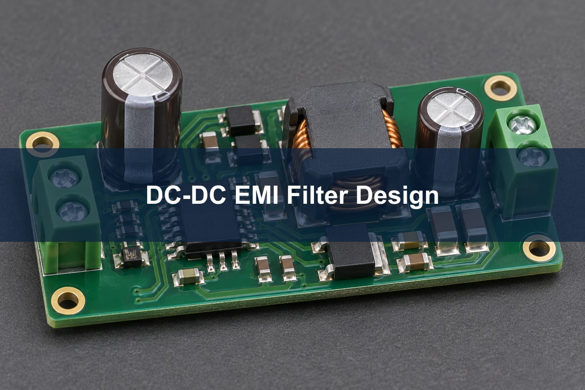
DC-DC converter board on an electronics bench
Illustrative rendering; not a photograph of a production or test setup.

For DC-DC EMI filter design, first measure which frequencies miss the conducted-emissions limit and determine how the noise returns. Use a differential-mode LC stage for noise between supply and return, and investigate common-mode paths when both wires carry noise in the same direction. Then check that the filter improves emissions without destabilizing the converter.

Consider a hypothetical 24 V industrial controller with a 400 kHz buck regulator. The engineering question is not how to build the largest filter. It is how to reduce noise on the power harness while preserving startup and load-step behavior. The numerical examples below are calculations, not measurements or compliance results.

EMI filter design for DC-DC converter

Start at the converter input and trace the switching current through its local bypass capacitor, switches and return. In a buck converter, the input current is pulsed. A capacitor beside the switching stage supplies much of that pulse locally; a filter at the input connector then reduces the part that reaches the power harness. Keep the unfiltered switching-side copper away from the connector-side copper so coupling does not bypass the filter.

Keep the local bypass in place while measuring the baseline. Removing it changes the circuit being evaluated. For this controller, identify the worst operating input and load, mark the first harmonic or frequency band that fails, and save the setup before changing any components.

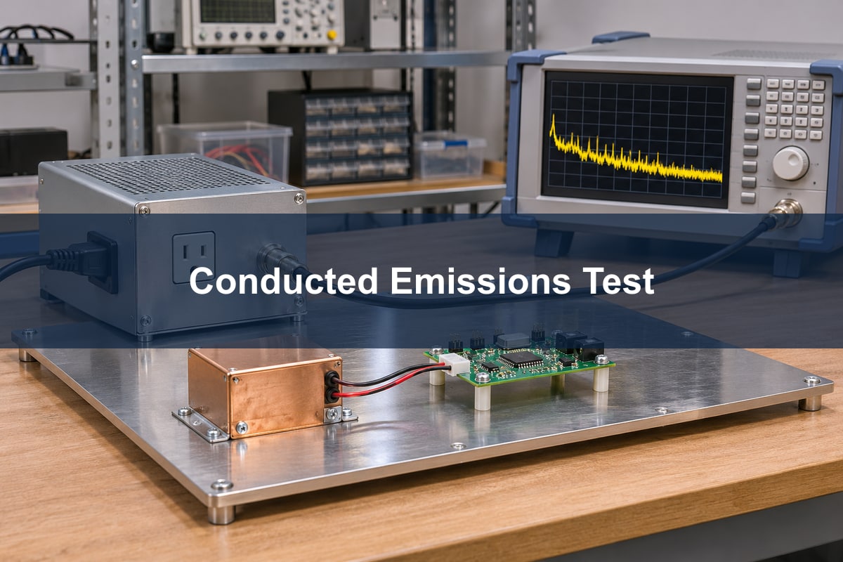
Conducted emissions test setup

Use the line impedance stabilization network (LISN), detector, bandwidth, grounding and harness specified for the product. A LISN makes the input impedance seen by the device more repeatable and couples the measured RF disturbance into the instrument. A bench supply and a long clip lead alone do not reproduce that measurement.

For a meaningful before-and-after check, hold the harness and load constant, measure the ambient floor, and capture the same operating modes with the same detector settings. Check that the measurement chain is not overloaded and that the setup follows the lab procedure. A pre-compliance scan is useful for design iteration; it is not a compliance claim.

Power supply conducted-emissions bench and DC-DC test board
Illustrative rendering; not a photograph of a production or test setup.

Common mode vs differential mode noise

Differential-mode current flows out on one power conductor and back on the other. Common-mode current travels in the same direction on both conductors and closes through another path, such as capacitance to chassis. A clamp around both power conductors together largely cancels equal and opposite differential current; a remaining signal suggests common-mode current if the probe arrangement and bandwidth support the measurement.

Observed clue Candidate path Change to test
Strong switching harmonic on individual lines, weaker with both inside the clamp Differential Test a damped LC stage and verify the local input bypass loop.
Peak remains with both lines in the clamp and shifts with chassis or cable placement Common mode Investigate coupling to chassis and trial a common-mode choke.
One band falls while another barely moves Mixed or frequency-dependent Test each band separately and check for bypass coupling.

Common mode choke filter

A common-mode choke uses coupled windings so equal and opposite load currents ideally cancel their flux, while common-mode currents see higher impedance. Select it using the impedance curve at the failing frequencies, continuous current and temperature rise. Leakage inductance adds some differential impedance, but it is not a controlled substitute for a separate differential stage unless characterized.

Before selecting a larger choke, inspect the alternative return path and the coupling from the switch node to chassis or a heat spreader. Changes to chassis capacitors may affect leakage current or isolation and must follow the product’s safety requirements. Recheck both noise modes because a layout change can alter how they couple.

EMI filter design calculation

An ideal 10 ”H and 10 ”F LC pair has an undamped resonant frequency of about 15.9 kHz, using 1/(2π√(LC)). If effective capacitance at the operating bias is 4 ”F instead, it is about 25.2 kHz. Neither result is the attenuation at 400 kHz.

Input Illustrative value How to validate
Filter inductance 10 ”H Check inductance versus current and impedance versus frequency.
Effective capacitance 10 ”F nominal; 4 ”F in bias example Use the selected part’s voltage and temperature curves.
Attenuation need 14 dB over limit + 6 dB chosen margin = 20 dB Recheck the failing frequency with the actual source, load and harness.

Inductor parasitics, capacitor ESR and ESL, source impedance, and converter input behavior all affect the real result. Use the calculation to choose parts for a prototype. Use the spectrum and stability checks to accept or reject that prototype.

EMI filter damping

Damp the input filter if its impedance peak can interact with the regulated converter. A converter drawing approximately constant input power can present a negative incremental input resistance over part of its operating frequency range: a small input voltage dip can make it draw more current. An undamped high-Q filter can amplify the resulting disturbance.

One candidate is a resistor in series with an auxiliary capacitor, placed across the filter output. The capacitor blocks continuous DC current through that resistor, while the branch can dissipate energy near resonance. Compare the filter output impedance with converter input impedance in the interaction region using the converter vendor’s method. Then measure startup and load steps across input voltage and load. Check that input ringing decays and voltage stays inside the converter’s operating limits.

EMI filter insertion loss

Insertion loss describes how much the signal falls when the filter is inserted in a specified fixture. A vendor curve obtained with standardized source and load impedances helps compare parts, but the supply, harness and operating converter do not necessarily match that fixture.

Compare the prototype and the baseline at each failing frequency under the same setup. Save the margin to the limit, not just the largest peak reduction. A filter that reduces a 400 kHz peak but raises a different band above the limit has not solved the release problem.

Conducted emission test failure reasons

When a filter does not improve the failing band, first confirm the mode, the fixture and the board’s operating state. If adding differential inductance does nothing while the paired-wire clamp still sees the peak, investigate common-mode coupling rather than continuing to increase inductance. If filter input and output run beside each other, move or shield the coupling path before changing values again.

Release the design only after meeting the applicable emissions limit across defined modes with the chosen margin, preserving startup and load-transient behavior, and recording the exact tested BOM and layout revision. For a separate introduction to passbands and cutoff, see the low-pass filter circuit guide.

FAQ

Can the same filter be used on a boost converter?

Not by default. Recheck which port has discontinuous current and where the failing noise is measured.

Will a ferrite bead replace the filter inductor?

Only if its impedance under bias covers the failing band without creating an unacceptable resonance or voltage drop.

Why did the circuit reboot after adding the filter?

Capture converter-pin voltage during startup. Inrush drop, source current limiting and filter resonance can look similar at the output.

Should an input TVS be treated as the EMI filter?

No. A TVS limits transient voltage; it does not provide predictable continuous attenuation for switching noise.

Can spread spectrum replace the filter?

It can redistribute narrowband energy, but the final detector results, other frequency bands and operating modes must still pass.

Can I use the same scan for every harness length?

Only if the test plan allows it. Cable placement and length can change common-mode paths and resonances.

Why can a part with low DC resistance still perform poorly?

DC resistance does not show its high-frequency impedance or how that impedance changes near self-resonance.

What should be retained for a design review?

Save baseline and final traces, the limit and detector settings, input and load conditions, harness photos, startup waveforms and the board revision.

References

Discuss a PCB design for manufacture

For a layout or fabrication review, send the connector and filter area, stack-up and board revision to sales@bestpcbs.com.

You may also like