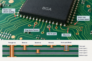
BGA PCB design succeeds when the package, fanout, stack-up, electrical constraints and manufacturing route are treated as one connected decision. A breakout that looks clean on screen can still fail if the land pattern uses the wrong package revision, the via structure is unavailable, return paths are broken, or hidden joints cannot be inspected. The design process must turn the exact ball map into a buildable PCB and assembly plan, supported by the data that EBest Circuit needs to review and quote the project.

What Should Be Checked Before Starting BGA PCB Design?
Start only after the exact package identity, ball map and manufacturing limits are controlled. BGA pitch is not enough to create a land pattern or choose a stack-up. The same nominal pitch can appear on packages with different ball diameters, depopulated regions, power fields, body sizes and vendor recommendations.
The design input set should answer six practical questions:
- Which package revision is being placed? The controlled record includes the full manufacturer part number, package code, drawing revision and approved pinout. A footprint copied from a similar device is not proof of compatibility.
- Where are the critical balls? Mark high-speed groups, clocks, differential pairs, memory interfaces, power, ground, sense pins, no-connects and reserved locations before choosing escape directions.
- What does the component vendor recommend? Reconcile the vendor’s board-land and routing guidance with the intended PCB and assembly processes.
- What can the proposed fabricator build? The capability review covers trace and spacing, drill structure, microvia spans, via filling, registration, copper weights and stack-up options.
- What must the assembler control? Assembly inputs cover solder-mask registration, stencil needs, package handling, thermal-profile constraints, neighboring-component clearance and hidden-joint inspection access.
- How will success be verified? Establish the electrical, thermal and assembly acceptance evidence before routing removes test access or forces an unsuitable inspection plan.
When an input remains provisional, label it as an open decision. That prevents an early routing assumption from silently becoming a released manufacturing requirement.
How Does BGA Pitch Affect Pad, Trace and Via Selection?
Pitch controls the physical space between balls, but it does not select the land, trace or via by itself. The usable routing channel also depends on the approved land diameter, solder-mask opening, copper tolerance, trace width, clearance and via geometry. A pitch value therefore cannot prove that a board needs HDI or that a particular trace width will fit.
Pad style belongs in the same decision. With a non-solder-mask-defined land, the mask opening is larger than the copper land and leaves the copper edge exposed. With a solder-mask-defined land, the mask opening defines the exposed soldering area. Neither style is universally better. The package recommendation, land geometry, mask registration, surface finish and assembly process determine which choice is appropriate.
As the available channel becomes tighter, ask the questions in this order:
- Pad: Does the land pattern match the exact package and the intended assembly process?
- Mask: Can the fabricator hold the required opening and web without creating registration or mask-sliver risk?
- Trace: Can a route pass through the remaining channel with the required clearance and electrical performance?
- Via: Is there space for a dog-bone transition, or must the via move into the land or use a build-up layer?
- Stack-up: Does the selected trace and via geometry still work with the impedance, copper and dielectric structure?
The deliverable is a manufacturer-reviewed geometry set for the BGA region, based on its actual package and fabrication constraints.
When Should You Use Dog-Bone, Microvia or Via-in-Pad Fanout?
The preferred fanout is the least complex structure that can escape the required balls and meet the design constraints. The decision is conditional: pitch affects the available space, but ball-map density, trace rules, stack-up access and reference continuity decide which structure actually works.
- Dog-bone fanout: This fits a package when a short trace can connect the land to a nearby plated through via without violating the land, mask, trace or clearance rules. It is often the most economical route, but the through via occupies space and creates antipads on every penetrated layer.
- Blind microvias: These fit inner rows that need denser escape when selected build-up layers provide enough routing access. The fabricator must confirm drill depth, capture lands, registration, copper filling and the permitted stacked or staggered structure.
- Via-in-pad plated over: This fits a layout when moving the transition into the BGA land provides needed escape density or a shorter electrical path. The via must be specified as a controlled filled, planarized and plated feature so the soldering surface is flat.
- Buried or combined via structures: These make sense only when the layer transition plan justifies the additional lamination and registration complexity. Adding every available via type without a clear routing purpose increases cost and failure opportunities.
A common mistake is to select via-in-pad because the package is described as fine pitch, then discover that the proposed shop cannot build the specified fill or layer span. The opposite mistake is forcing through vias into a dense field and losing the power-plane area or signal channels needed on deeper layers. A fabricator review of a sample fanout should occur before the rest of the device is completed.

How Many PCB Layers Are Needed for BGA Escape Routing?
There is no reliable layer-count formula based only on ball count or pitch. Layer demand comes from the number and location of balls that must escape, the channels opened by the chosen fanout, route direction, reference-plane needs, power distribution and the fabrication structure.
Begin with a marked ball map. Assign perimeter signals that can leave on surface layers, identify inner rows that require vias, reserve paths for critical interfaces, and keep power and ground fields visible rather than counting them as ordinary signals. Next, sketch the escape direction for each signal layer and check whether the adjacent reference remains continuous.
For example, adding a routing layer may not solve congestion if through-via antipads still block the same channels. A blind-via build-up may release those channels, but it changes lamination, cost and allowable layer transitions. A useful stack-up estimate therefore shows:
- which ball groups leave on each signal layer;
- which plane provides the return path for that layer;
- where signals change reference layers and need nearby ground transitions;
- how much plane copper is removed by via pads and antipads;
- which via spans and impedance structures the fabricator has accepted.
The stack-up can be closed after a representative inner-row breakout passes routing, plane-integrity and manufacturing review. This verification exposes residual congestion risk and avoids paying for extra layers that do not add usable escape capacity.
How Should BGA Escape Routing Protect Signal Integrity?
The breakout is part of the electrical channel and needs the same constraint discipline as the main route. Narrow neck-down traces, via barrels, antipads, reference changes and crowded return paths can create discontinuities before a signal reaches its normal controlled-impedance geometry.
A differential pair needs a symmetric escape path. Unequal fanout routes, different layer-change locations or a split reference can add skew and mode conversion while forcing return current onto a longer path. Reserve comparable transitions for both members and keep a continuous reference with nearby return vias.
The same cause-and-effect check applies to other interfaces:
- A long unused through-via stub can become electrically significant on a bandwidth-sensitive channel; model it and consider a different via span or backdrilling when justified.
- An abrupt neck-down changes impedance; include the actual breakout geometry in the channel model instead of assuming the main-route width represents the whole interconnect.
- A dense via field can create reference-plane voids and coupling between transitions; inspect antipad interaction, return-via placement and local plane continuity.
- Routing critical lanes last may force avoidable transitions and detours; reserve their channels before low-speed nets consume them.
The relevant loss, impedance, skew and transition limits come from the component or interface design guide. Geometry that is acceptable for a control signal may not be acceptable for a clock, memory strobe or high-speed serial lane.
How Should Power, Ground and Decoupling Be Planned Under a BGA?
A BGA can escape every signal and still have an inadequate power-distribution network. Power and ground balls need short, distributed transitions into usable plane copper, and each decoupling connection needs a low-inductance current loop appropriate to its rail.
A complete rail map identifies every supply, ground, analog rail, sense connection and reserved power pin in the approved ball map. The via field can then be reviewed as a current path rather than a routing obstacle. Too few power vias can concentrate current; oversized antipads can narrow a plane; poorly placed signal transitions can divide the copper that the package needs.
- At the package: distribute power and ground vias across the corresponding ball fields instead of collecting a rail through one narrow exit.
- At the planes: inspect the copper remaining after antipads, clearances and route channels are applied.
- At the capacitors: minimize the loop formed by the supply terminal, its via, the plane pair, the return via and the ground terminal within the available placement area.
- At transitions: add return vias near signal layer changes so return current does not detour around plane openings.
- At verification: evaluate voltage drop and impedance using the real stack-up, device current profile and capacitor models where the product risk requires it.
A fixed capacitor count or distance is not a substitute for this analysis. Package inductance, rail targets, capacitor behavior, mounting geometry and board construction all affect the result.
How Can BGA PCB Design Reduce Thermal and Warpage Risk?
Thermal and mechanical decisions should control device temperature without creating board bending or solder-joint strain. More copper and more thermal vias may improve heat spreading, but an asymmetric copper field or a heavy local structure can also change board stiffness and warpage.
The thermal review starts with the approved power and operating case, then follows the heat path through package lands, board copper, thermal vias, planes, airflow and any heat-spreading interface. Its interaction with the rest of the board includes:
- Copper balance: large local plane differences and uneven panel copper can contribute to bow and twist, so review distribution with the fabricator.
- Via placement: thermal vias should support the intended heat path without removing excessive plane copper or disrupting signal return paths.
- Board support: mounting points, connectors and stiffeners should not impose bending loads through the BGA region during assembly or service.
- Component neighborhood: tall parts, shields and connectors can block airflow or rework access and can impose a different thermal mass during soldering.
- Reflow behavior: the assembler should develop the profile for the actual package and board rather than reusing a profile from a smaller or less massive assembly.
High-risk products may require temperature measurement, warpage characterization, strain measurement or environmental testing. The applicable method and limit should come from the component, product or validated process requirement, not from a generic BGA claim.
Which DFM Checks Should Be Completed Before BGA PCB Fabrication?
DFM should prove that the released design can be fabricated and assembled as specified before tooling begins. This chapter owns pre-production corrections; it does not use later X-ray images as a substitute for closing design errors.
- Footprint identity: compare copper lands, solder-mask openings, paste intent, courtyard and orientation marks with the exact package revision.
- BGA-region geometry: run the proposed shop’s trace, spacing, annular-ring, drill-to-copper and mask-registration rules on the real fanout.
- Via construction: document drill type, layer span, fill, planarization, plating and any backdrill requirement. The stack-up must support every transition.
- Stack-up and impedance: obtain a manufacturable material and copper proposal, then update the controlled geometry rather than releasing an unconfirmed nominal stack-up.
- Plane and return paths: review antipad fields, splits, necked power areas and reference changes under and around the package.
- Assembly access: check stencil feasibility, neighboring clearances, component orientation, fiducials, thermal mass, rework envelope and access for the planned inspection method.
- Data consistency: compare fabrication output, drill data, assembly drawing, BOM and placement data against the same design revision.
Each open item needs an owner and a disposition in the released files. A verbal shop-floor workaround may solve one build but leaves the next lot exposed to the same ambiguity.
What Assembly Controls Reduce BGA Soldering Defects?
Good assembly control begins with board data that allows consistent paste transfer, placement and heating. The design-related controls below address PCB and package decisions that change the risk of opens, bridging, voiding, head-in-pillow and rework damage.
Paste deposition: land geometry, via-in-pad flatness, stencil design and local board topography affect the amount and uniformity of paste delivered to the joint. An open or depressed via in a solder land can pull solder away from the interface.
Placement and handling: clear orientation marks, usable fiducials, controlled package moisture handling and adequate neighboring clearance reduce placement and rework errors. If underfill or reinforcement is required, its access and inspection consequences need to be considered during layout.
Thermal profile: package size, board copper, shields and nearby thermal masses influence heating across the BGA. The assembler should validate the profile on the representative build rather than assuming that one profile fits every board.
Change control: substitutions in package code, surface finish, stencil, paste, board supplier or via construction can change soldering behavior. These changes remain tied to an approved revision and trigger the affected process verification again.
How Should BGA Solder Joints Be Inspected and Tested?
A risk-based combination of process records, imaging and electrical tests provides stronger evidence. No single method proves every hidden-joint condition, and not every PCBA needs every inspection method.
- SPI can confirm solder-paste deposition before placement when the process plan includes it, helping catch volume or alignment problems before the joints become hidden.
- AOI can verify visible placement, polarity and nearby solder features, but it cannot directly see the full joint field beneath a BGA.
- X-ray can reveal selected hidden features such as alignment, bridging patterns and void distribution. The plan should state the required views, observable features, acceptance criteria and sampling.
- ICT, flying probe or boundary scan can provide electrical coverage when the design exposes meaningful access or device support.
- Functional testing checks behavior at product level against an approved procedure, but a passing function does not explain every latent solder condition.
- Cross-section or dye-and-pry may support qualification or failure analysis when non-destructive evidence cannot resolve the cause.

When a defect is found, the corrective action should connect it back to the design and process evidence. A change to the land, via fill, stencil, profile, board support or package handling needs to answer the observed failure mechanism and produce evidence on the next build.
What Files Are Needed for BGA PCB Manufacturing and Assembly?
A manufacturer can review and quote the project accurately only when the package, PCB, assembly and test data describe the same revision. The review package therefore contains enough information to reproduce the intended product rather than only a screenshot of the BGA breakout.
- Component and package data: manufacturer part number, package drawing, ball map, land guidance, thermal data and device-specific PCB instructions.
- PCB design data: native layout or agreed intelligent exchange, schematic, net classes, constraints and controlled library identity.
- Fabrication package: Gerber or ODB++, drill files, drawing, stack-up, material notes, copper, impedance targets, via construction and acceptance criteria.
- Assembly package: controlled BOM, centroid or placement data, assembly drawing, polarity/orientation information, stencil notes and any approved substitutions.
- Inspection and test requirements: required X-ray views or criteria, test method, test files, fixtures, programming data and expected records.
- Commercial inputs: prototype and production quantities, panel or delivery preference, schedule target, packaging, traceability and documentation needs.
A quote should show what is included across PCB fabrication, components, BGA assembly, tooling, inspection, testing, special processes, packaging and freight. The lowest unit price is not the lowest project cost if essential controls or one-time items are omitted.
How Can EBest Support Fine-Pitch BGA PCB Manufacturing and Assembly?
EBest Circuit can review and quote a connected route from PCB DFM through fabrication, component sourcing, BGA assembly and agreed verification. The land pattern, via structure, stack-up and assembly requirements can then be resolved against one controlled data package before production decisions become expensive to change.
- DFM review: fewer late manufacturing changes. The returned findings identify open pad, mask, via, clearance and data-consistency issues from the package drawing, ball map, stack-up and layout before tooling.
- PCB fabrication: a route matched to the fanout. The quoted stack-up and via construction can be checked against the actual breakout instead of treating HDI, via-in-pad or backdrilling as labels.
- Component sourcing: controlled package identity. The BOM and approved manufacturer part number keep the assembled package aligned with the footprint and ball map used in design.
- BGA assembly: design and process coordination. Stencil, via-in-pad surface, placement access, package handling and thermal-profile needs can be reviewed with the board data.
- Applicable X-ray: hidden-joint evidence. Where the package and risk plan require it, the quotation can state the inspection scope and expected output instead of assuming that a generic X-ray statement is sufficient.
- Agreed testing: product-specific coverage. The intended ICT, flying-probe, programming or functional-test inputs allow feasibility and deliverables to be confirmed before the order.
This support remains project specific. Final pad dimensions, via structures, process controls and inspection criteria depend on the component, board design and approved customer requirements.
FAQs About BGA PCB Design
These answers address common boundary questions without turning them into universal layout rules. The final decision still belongs to the actual package, board stack-up and manufacturing route.
Q1: What BGA pitch is considered fine pitch?
A1: No single pitch threshold determines the PCB process. The usable pad, mask, trace and via geometry, together with the ball map and supplier capability, matters more than a label.
Q2: Can a 0.5 mm pitch BGA be routed without HDI?
A2: It is possible on some packages and board builds. Depopulated regions, outer-row access, allowed trace and spacing, land size and the exact pinout can make a conventional route practical; dense inner rows may still require microvias or via-in-pad.
Q3: Can plugged vias be placed under a BGA?
A3: Yes, when the approved via structure creates the required soldering surface. The fabricator must control the fill, planarization and plating; an unspecified plug is not equivalent to plated-over via-in-pad.
Q4: Is ENIG suitable for BGA assembly?
A4: ENIG can be suitable when its specification and process match the assembly. Select the surface finish with shelf-life, soldering, planarity and product requirements rather than by package name alone.
Q5: Can 3 mil traces be used for BGA escape routing?
A5: Only when the fabricator accepts the geometry and it meets the design requirements. Copper, clearance, impedance and reliability still apply; a width used in one stack-up should not become a universal rule.
Q6: Why does via-in-pad increase PCB cost?
A6: It can add several controlled fabrication operations. Drilling, filling, planarization, plating, inspection and possibly sequential lamination depend on the via span, board build and supplier process.
Q7: Can a BGA be reworked after assembly?
A7: Rework may be possible when the layout and an approved process permit it. Review component access, neighboring clearances and board thermal behavior before release, especially on dense or thermally massive boards.
Q8: Can AOI inspect BGA solder joints?
A8: AOI cannot directly see the hidden joint field. It can check visible placement and surrounding features, while hidden joints normally require another method such as X-ray plus appropriate electrical evidence.
Q9: When is backdrilling useful near a BGA?
A9: It can help when an unused through-via stub affects a bandwidth-sensitive transition. The stack-up, drill access and reliability plan must support it; it is not required for every BGA net.
Q10: What should be sent for a BGA PCB quotation?
A10: Send one revision-controlled package that defines the board, assembly and expected evidence. Include the package information, PCB data, BOM, placement files, quantities, inspection/test requirements and required records.
Conclusion: How Can You Reduce BGA PCB Design Risk Before Production?
BGA risk falls when package, fanout, layer, electrical, thermal and manufacturing decisions are resolved in dependency order. A controlled BGA PCB design process verifies pad and fanout geometry, protects signal and power paths, closes DFM findings and establishes assembly evidence while the footprint, via structure and stack-up can still change.
A free DFM review is available through sales@bestpcbs.com when the package drawing, ball map, native layout or fabrication data, BOM, quantities and inspection/test requirements are ready. EBest Circuit returns the open design inputs, proposed PCB and assembly route, and the evidence to include in the quotation, giving your team a clearer basis for approving the build.