PCB manufacturing PCB manufacturing
Home > Blog

What is FR4 material in PCB? – EBest Circuit (Best Technology)

July 12th, 2024

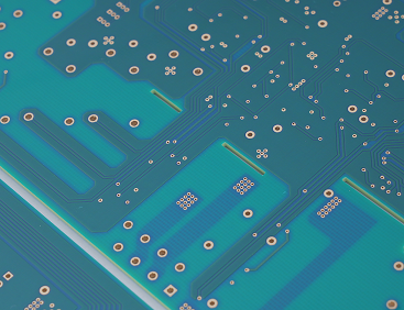
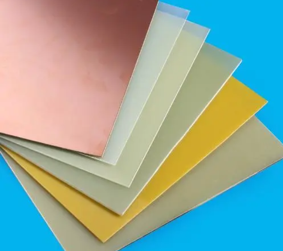
FR4 is a commonly used material in the printed circuit boards (PCBs) manufacturing. If you’re in the electronics field, you’ve likely heard of it. It is the footstone of a circuit board, provides good mechanical strengthen and electrical insulation properties. Today, we will share informational about FR4 material, its types, advantages and alternatives. Keep reading if you are interested in.

What is FR4 material in PCB? - EBest Circuit (Best Technology)

What does FR4 stand for?

FR4 stands for “Flame Retardant 4”, also called FR-4 Epoxy Glass Cloth by PCB manufacturers. It is not a material name, but a material grade, so there are many types of FR-4 grade materials used in general circuit boards. But most are composites made with so-called Tera-Function epoxy resins plus fillers and glass fibers. FR4 is made from woven glass-reinforced epoxy resin. The typical composition of FR4 includes approximately 60% glass fabric and 40% epoxy resin by weight.

What is FR4 material in PCB? - EBest Circuit (Best Technology)

This composite material is known for its high mechanical strength and flame-retardant properties. The “4” in FR4 signifies the level of flame retardancy. It means the material is resistant to catching fire, which is critical in preventing electrical fires in electronic devices.

What are the classifications of FR4 materials?

FR4 materials are classified based on various properties and specifications to cater to different applications and requirements. These classifications help in selecting the right type of FR4 material for specific PCB needs. Here are the primary classifications of FR4 materials:

1. Standard FR4

Standard FR4 is the most commonly used classification. It offers a good balance of electrical insulation, mechanical strength, flame retardancy, and cost-effectiveness. Standard FR4 materials have a glass transition temperature (Tg) typically around 130°C to 140°C. They are suitable for general-purpose PCBs used in consumer electronics, industrial controls, and telecommunications equipment.

2. High Tg FR4

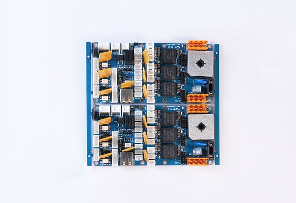
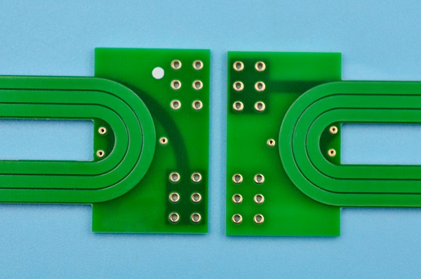
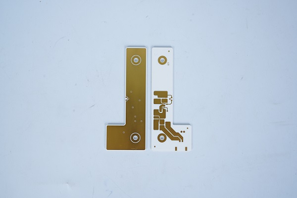
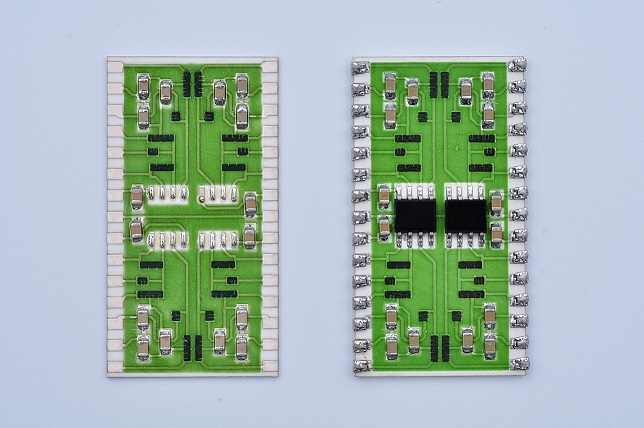
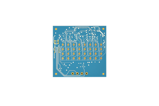
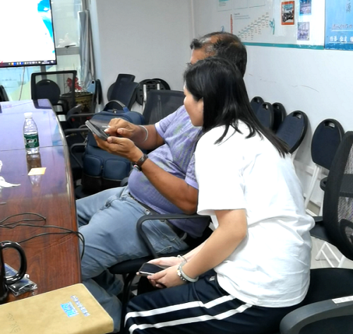
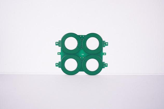
High Tg FR4 materials are designed for applications requiring higher thermal performance. These materials have a higher glass transition temperature, usually above 170°C. High Tg FR4 is used in applications where the PCB is exposed to higher temperatures, such as automotive electronics, aerospace, and high-power devices. The increased Tg provides better stability and performance at elevated temperatures. This is the high Tg FR4 PCB that we made before.

3. Low Dk FR4

Low Dk (Dielectric Constant) FR4 materials are used in high-frequency applications where signal integrity is crucial. So, we called it as “High-frequency FR4”. These materials have a lower dielectric constant, which reduces signal loss and improves signal transmission. Low Dk FR4 is often used in RF and microwave circuits, where maintaining signal integrity is essential.

4. High CTI FR4

High CTI (Comparative Tracking Index) FR4 materials have an improved resistance to electrical tracking. These materials are used in applications where the PCB is exposed to high voltages and harsh environments. High CTI FR4 provides better insulation and reduces the risk of electrical failure due to tracking.

5. Halogen-Free FR4

Halogen-free FR4 materials are designed to meet environmental and safety requirements by eliminating halogens. Which can be harmful if released during PCB manufacturing or disposal. These materials are used in applications where reducing environmental impact is a priority. Halogen-free FR4 offers similar performance to standard FR4 but without the use of halogenated flame retardants.

Benefits of using FR4 as PCB material

  • Excellent Electrical Insulation
  • High Mechanical Strength
  • Flame Retardancy
  • Moisture Resistance
  • Cost-Effectiveness
  • Thermal Stability
  • Ease of Fabrication

Properties of FR4 material

PropertyParameter
Vertical flexural strengthNormal State: E-1/150, 150±5℃≥340Mpa
Parallel layer impact strength≥230KJ/m
Insulation resistance after water immersion (d-24/23)≥5.0×108Ω
Vertical electrical strength≥14.2MV/m
Parallel layer breakdown≥40KV
Relative Dielectric Constant (50hz)≤5.5
Relative Dielectric Constant (1mhz)≤5.5
Dielectric Loss Factor (50hz)≤0.04
Dielectric Loss Factor (1mhz)≤0.04
Water Absorption (D-24/23, 1.6mm Thickness)≤19mg
Density1.70-1.90g/cm³
FlammabilityFV0

What is the Difference Between IMS and FR4 PCB?

IMS (Insulated Metal Substrate) and FR4 PCBs serve different purposes. IMS PCBs are designed for applications requiring efficient heat dissipation. They have a metal base layer that helps manage heat more effectively than FR4. This makes IMS ideal for high-power applications like LED lighting.

IMS insulated metal substrate PCB

On the other hand, FR4 PCBs are used in general electronic applications due to their balance of performance and cost. While IMS excels in thermal management, FR4 is preferred for its electrical properties and versatility.

What is the Cost of FR4 PCB Per Square Inch?

The cost of an FR4 PCB can vary based on several factors. These include the board’s thickness, the number of layers, and the complexity of the design. On average, the cost per square inch of FR4 PCB ranges from $0.10 to $0.50. However, this is a rough estimate. For a precise quote, it’s best to contact PCB manufacturers with your specific requirements. If you are searching for a PCB supplier, EBest Circuit (Best Technology) is here to waiting for you.

Why is Rogers Better Than FR4 Material?

Rogers material is often considered superior to FR4 in high-frequency applications. Here are some key reasons why Rogers might be chosen over FR4.

  1. Lower Dielectric Loss
  2. Higher Thermal Conductivity
  3. Improved Dimensional Stability
  4. Consistent Dielectric Constant
  5. Superior Performance in High-Frequency Applications
  6. Compliance with Stringent Industry Standards

What Material is Similar to FR4?

Several materials are similar to FR4 and can be used as alternatives. One such material is CEM-1, which is also a composite material made from epoxy and fiberglass. It offers good mechanical strength and electrical properties but is less flame retardant than FR4.

Another alternative is polyimide, known for its excellent thermal stability and flexibility. It is often used in applications requiring high-temperature resistance. However, polyimide is more expensive than FR4. For specific applications, materials like PTFE (Teflon) can also be considered, especially in high-frequency applications.

FAQs

1. Can FR4 be used in high-temperature applications?

FR4 can withstand moderate temperatures, but for high-temperature applications, materials like polyimide are preferred.

2. Is FR4 environmentally friendly?

FR4 is not biodegradable but can be recycled to some extent. Proper disposal and recycling methods should be followed.

3. How does the thickness of FR4 affect PCB performance?

The thickness of FR4 can impact the board’s mechanical strength and thermal dissipation. Thicker boards offer more durability but may also increase the cost.

4. Are there any disadvantages to using FR4?

FR4 has limitations in high-frequency and high-temperature applications. It is also less effective in thermal management compared to materials like IMS.

5. Can FR4 PCBs be used in flexible circuits?

FR4 is rigid and not suitable for flexible circuits. For flexible applications, materials like polyimide are used. But recently, EBest Circuit (Best Technology) developed a new product called “semi-flexible FR4 PCB”, its flex area is made by FR4 material.

  • Is FR4 RoHS Compliant?

Yes, FR4 is RoHS compliant. This means that it meets the regulations set by the European Union to limit the use of specific hazardous materials found in electrical and electronic products.
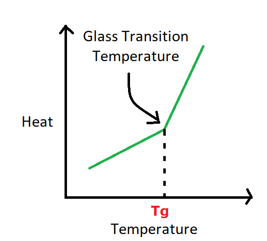
  • What is FR4 Tg?

The glass transition temperature (Tg) of FR4 is a critical property that indicates the temperature at which the material transitions from a hard, glassy state to a soft, rubbery state.

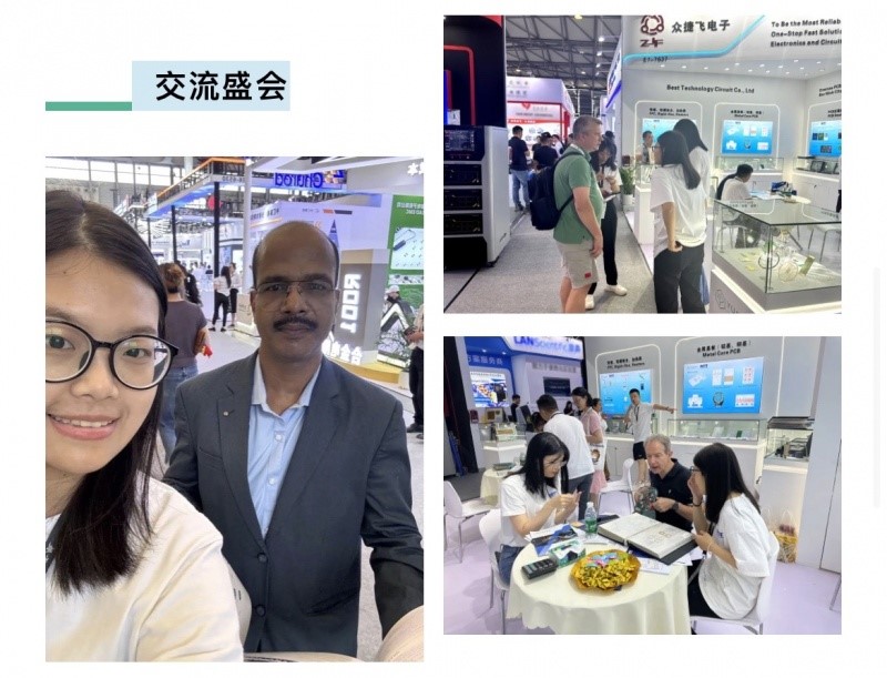
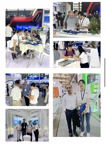
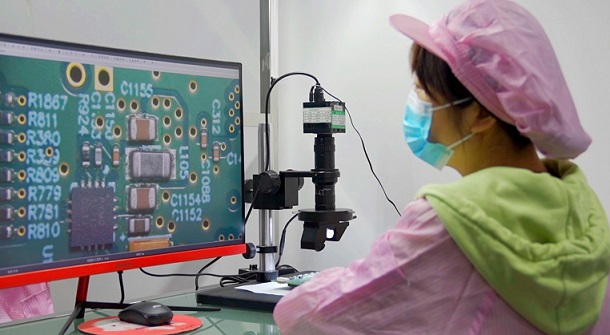
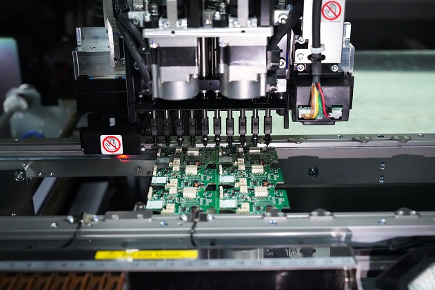
EBest Circuit (Best Technology) excels not only in PCB and assembly manufacturing, but also in offering top-quality PCB design services. Our professional engineering team is ready to support your innovation across various industries, including communications, healthcare, industrial, and consumer electronics. We welcome all the questions or inquiries from you.

A Perfect Ending in Electronica China 2024! – EBest Circuit (Best Technology)

July 11th, 2024

During July 8th to 10th, EBest Circuit (Best Technology) had an exhibition at the Electronica China 2024, and now, we are so excited to share that we had an incredible time! It was our first time at this event, and we believe it is not the last time.

It is must to say that the Electronica the perfect place for us to show off our cutting-edge PCB products. Our booth was buzzing with visitors curious about our advancements in metal core PCBs, ceramic PCBs, flexible PCBs and PCB design. We were thrilled with the positive feedback and the high interest in what we had to offer.

The exhibition wasn’t just about our products; it was also about making meaningful connections. We got to chat with industry experts, potential clients, and fellow exhibitors, discussing the latest trends and exploring possible collaborations. These conversations were incredibly valuable, and we’re excited to keep these relationships growing.

At this exhibition, EBest Circuit (Best Technology) also attracted the attention of authoritative media such as CCTV (China Central Television). It is a big and famous media in China. CCTV reporter visited our booth and conducted an interview with our founder, Peter. During the interview, Peter introduced the company’s latest products and technical advantages in detail, and shared the successful experience and future development plan of Best in the industry.

We want to send a huge thank you to all the friends and visitors who stopped by our booth. Your support and interest mean so much to us. Your enthusiasm for our products has motivated us to keep pushing the boundaries and coming up with even better solutions.

If you didn’t get a chance to see us at Electronica China 2024, don’t worry! We’ve got more exciting exhibitions lined up. You can catch us at PCB West in October and in Munich, Germany in November. We can’t wait to meet more industry pros and show off our latest innovations at these events.

EBest Circuit (Best Technology)’s debut at Electronica China 2024 was a big success. We’re so grateful for the opportunity to share our products and connect with the industry community. Thanks again to everyone who visited our booth. We look forward to seeing you at our upcoming exhibitions!

How to Make a BOM?

July 11th, 2024

If you are familiar with SMT or PCB assembly process, you may know BOM file. It is an important element in the SMT process. Creating BOM is a crucial step in the manufacturing process, especially for PCBs. A BOM serves as a comprehensive list of all the parts, components, and materials needed to build your product. It ensures that everyone involved in the production process is on the same page, reducing the risk of errors and delays. Today, EBest Circuit (Best Technology) would like to introduce BOM and giving you a guide to create a BOM file step by step.

How to Make a BOM?

What is a Bill of Materials (BOM)?

A Bill of Materials (BOM) is a detailed list of all the parts, components, and materials needed to manufacture a product. In PCB manufacturing, a BOM outlines every item required to assemble a PCB, including quantities, part numbers, and descriptions. It serves as a guide to ensure that the manufacturing process runs smoothly and that no crucial components are missing.

Types of Bill of Materials

There are several types of BOMs used in different stages of production. Each type serves a specific purpose and provides unique details to streamline processes and ensure accuracy. Here are the primary types of BOMs:

  • Engineering BOM

This type of BOM is creating during the design phase. It lists all the parts and components designed by the engineering team, including specifications and relationships as intended in the final product. And of course, it mainly used by design engineers to communicate the product structure and details to manufacturing teams.

  • Manufacturing BOM (Formal)

It is a formal BOM files that used in the assembly phase. Different with engineering BOM, it includes additional details necessary for manufacturing, such as packaging, handling instructions and assembly details. And some special instructions.

  • Sales BOM

Sales BOM is used by sales teams and includes information relevant to the sales process, such as pricing and availability. It helps in providing accurate quotes, managing customer expectations, and handling sales orders efficiently.

What Should Include in an Effective Bill of Materials?

An effective BOM should be detailed, accurate, and easy to understand. It should include all the details of components and indicated revisions. As a 18 years expertise in PCBA production, we summarized the key elements that should be included in the BOM.

  • Component details

It should include all the components and their detailed information, such as names, part numbers (PN), and descriptions for each part.

  • Quantity (QTY)

The exact quantity of each component required for the product. Accurate quantities can prevent shortages and overstocking.

  • Foot print

It is the package of each component, helping to ensure the correction of part.

  • Reference Designators

Unique identifiers that match each component to its specific location on the product layout. These are essential for assembly and troubleshooting.

  • Manufacturer Information

Manufacturer information, including the manufacturer name of components and manufacturer part number. It helps to ensure correct parts are sourced. And convenient for alternative part sourcing if it is shortage.

  • Supplier information (Optional)

It means the name of the supplier or distributor. The part number used by the supplier, which may differ from the manufacturer’s part number.

  • Assembly instructions

Any special notes for assembly such as DNF remark, and version control to track revisions should also be included. Additionally, cost information helps in budgeting, and lifecycle status information helps plan for component availability and avoid discontinued parts.

How to Make a PCB Bill of Materials (BOM)?

Creating a PCB BOM is a systematic process that involves compiling all the necessary information about each component required for the assembly of the PCB. Here’s a detailed guide on how to create a PCB BOM:

  • Open a Blank Spreadsheet

Use software like Microsoft Excel or Google Sheets to start with a blank spreadsheet. They are common to use, offering flexibility and ease of use for creating and managing BOMs.

  • Define Columns

Set up your spreadsheet with appropriate column headers. Common headers include:

  • Part Number
  • Component Name
  • Quantity
  • Reference Designator
  • Manufacturer
  • Manufacturer Part Number
  • Supplier
  • Supplier Part Number
  • Description
  • Package Type
  • Cost
  • Notes
  • Input Data

Enter the required details for each component under the appropriate headers. Please be make sure that all information is accurate and complete. This may involve referencing design files, datasheets, and supplier catalogs. If it is incorrect, then it needs a lot of time to find out and revise the errors, resulting in schedule delay.

  • Use Formulas

Utilize Excel formulas to automate calculations, such as summing total quantities or calculating costs. This helps in reducing manual errors and saves time.

  • Format for Clarity

Use cell formatting options to highlight important information and ensure the spreadsheet is easy to read. For example, you can use bold text for column headers, color coding for different component types, and borders to separate sections.

  • Include Version Control

Add a version control section to your BOM to track revisions and updates. This can be a simple row at the top or bottom of the spreadsheet, indicating the version number, date of revision, and a brief description of changes.

How to Make a BOM?
(BOM file reference)
  • Save and Update

Save your BOM and update it regularly to reflect any changes in the design or component availability. Regular updates ensure that the BOM remains accurate and up-to-date, preventing issues during production.

  • Review and Verify

Have multiple team members review the BOM for accuracy. Cross-check all component details, quantities, and part numbers against the design files. Verification helps catch errors early and ensures the BOM is reliable.

  • Communicate with Suppliers:

Maintain open communication with suppliers to confirm component details and availability. This ensures that you can source the correct parts and avoid delays in the production process.

How Can I Optimize My BOM for PCB Assembly?

Sometimes, a simple BOM is not good to process PCB assembly process, and manufacturers may need to spend a lot of time to optimize it, make into convenient for manufacturing. If you are a layman, here are some steps to help you in optimizing your BOM file.

First, it’s a good idea to standardize components where possible. Using standard parts that are readily available from multiple suppliers can simplify procurement and reduce costs. This approach minimizes the risk of shortages and ensures you can get parts quickly and affordably. Also, make sure all entries in your BOM are clear and concise to avoid confusion during assembly. Double-checking part numbers and quantities against design files is crucial to prevent errors that could lead to rework or delays.

Building strong relationships with your suppliers is another key factor. Good communication with suppliers helps ensure reliable component availability and keeps you informed about any changes in lead times or part availability. Regularly updating your BOM to reflect any design changes or component availability issues is essential. Keeping your BOM current and accurate prevents last-minute surprises during assembly.

How to Make a BOM?

What Common Mistakes Should I Avoid When Creating a PCB BOM?

Avoiding common mistakes in BOM creation can save time and reduce errors. Here are some pitfalls to watch out for:

  • Incomplete information – ensure all necessary details are included for each component.
  • Incorrect quantities – double-check quantities to avoid shortages or excess inventory.
  • Outdated data – keep the BOM updated with the latest design changes and component information.
  • Ambiguous descriptions – provide clear and precise descriptions to prevent confusion.
  • Lack of version information – implement version control to track changes and ensure the correct BOM version is used.

Creating an effective and accurate PCB BOM is essential for smooth manufacturing and assembly. By following best practices and using the right tools, you can ensure your BOM is comprehensive, clear, and up-to-date, ultimately leading to a successful PCB production process.

EBest Circuit (Best Technology) is an expert in SMT and PCB assembly, we have more than 18 years in this industry, that can offer you a best experience of PCBA solution. In our facotry, we have advanced equipment like full auto pick and place machine, online dual AOI, X-ray, 3D SPI, nitride reflow oven and three-proof paint machine. So that we can ensure the fast lead time and high quality of your PCBA products. Reach us to get a instant quote!

What is Tg meaning in FR4 PCB? – EBest Circuit (Best Technology)

July 10th, 2024

In the world of printed circuit boards (PCBs), understanding material properties is crucial. One such property is Tg, or glass transition temperature. For FR4 PCBs, knowing what Tg means can significantly impact design and performance. In this blog, we’ll explore what Tg is, how it’s measured, its importance, and other related questions.

What Does Tg Mean in PCB Manufacturing?

Tg stands for glass transition temperature. It refers to the temperature at which a polymer material, such as the resin in a PCB substrate, transitions from a hard, glassy state to a softer, rubbery state.

For the circuit board, the ‌Tg value reflects the highest temperature it can withstand. When the temperature exceeds Tg values, ‌ the molecular structure of the circuit board material will be changed, ‌ lead to changes in its physical properties. Such as mechanical strength, size stability, adhesive, water imbibition, thermal expansion, etc. ‌Therefore, the level of TG value of the PCB directly affects the stability and high temperature resistance of the circuit board.

What is Tg meaning in FR4 PCB? - EBest Circuit (Best Technology)

In the high temperature environment, if the TG value of the circuit board is too low, it is easy to cause PCB deformation, fracture, cracking and other problems, affecting the reliability and life of the printed circuit board. If the TG value of the circuit board is too high, the PCB is easy to become hard and brittle, affecting the processability and flexibility of the circuit board.

How is Tg Measured in FR4 Materials?

Accurate measurement of Tg is crucial for ensuring the performance and reliability of FR4 PCBs. Knowing the exact Tg helps in selecting the appropriate material for specific applications, particularly those involving high temperatures and thermal cycling. Using materials with a Tg well above the operating temperature ensures the PCB will maintain its mechanical and electrical properties under expected conditions.

The primary method for measuring Tg in FR4 materials is by differential scanning calorimetry (DSC). It involves heating a small sample of the material at a controlled rate, typically between 10°C to 20°C/min. As the sample heats, the DSC measures the heat flow into the material and records it as a thermogram. The Tg is identified as the temperature where there is a noticeable change in heat capacity, appearing as a step or inflection point on the thermogram. DSC is widely used because it provides precise and reliable Tg measurements.

What is Tg meaning in FR4 PCB? - EBest Circuit (Best Technology)

Additionally, Dynamic Mechanical Analysis (DMA) and Thermomechanical Analysis (TMA) also can be used to measure the Tg value.

Why is Glass Transition Temperature Critical in PCBs?

Glass transition temperature is critical because it affects the thermal and mechanical properties of the PCB. If a PCB operates near or above its Tg, it can experience issues like delamination, warping, and electrical failure. Here are some benefits of Tg.

  • Thermal stability

One of the main reasons is its role in determining thermal stability. During operation, PCBs are subjected to varying temperatures due to power dissipation from electronic components and environmental conditions. Make sure the Tg of the PCB material is well above the maximum operating temperature, it helps maintain mechanical stability and reliable performance under thermal stress.

  • Mechanical Strength

The Tg value also affects the mechanical strength and durability of the PCB. Below the Tg, the material is rigid and can withstand mechanical stress without significant deformation. This rigidity is essential for maintaining the structural integrity of the PCB, especially during assembly processes like soldering, where the board is subjected to mechanical and thermal stresses.

  • Thermal Management

Thermal management is very important to electronics, especially for those miniaturized electronic devices. If the PCB itself has good thermal management, then designers no need to install heatsink or coolers. Materials with higher Tg values exhibit lower coefficients of thermal expansion (CTE), meaning less expansion and contraction with temperature changes. 

  • Application-specific requirements

Different applications have varying thermal and mechanical requirements. High-performance computing, automotive, aerospace, and industrial electronics often operate in environments with high temperatures and thermal cycling. For these applications, using PCB materials with appropriate Tg values is crucial.

What is the Typical Tg Value for Standard FR4 PCBs?

Standard FR4 materials generally have Tg values in the range of 130°C to 140°C. For high-performance applications, materials with higher Tg values are necessary. The table below lists some common high Tg materials used in PCB manufacturing, along with their Tg values and characteristics.

MaterialTg Value (°C)CharacteristicsApplications
ISOLA IS410180Excellent thermal and mechanical propertiesHigh-reliability applications
Nanya NP-175175High thermal stability, good mechanical strengthAutomotive, industrial electronics
Shengyi S1000H170Cost-effective, widely usedConsumer electronics, industrial applications
Ventec VT-47170High Tg and low CTEHigh-density interconnect (HDI) PCBs
Rogers 4350B280Extremely high Tg, excellent thermal stabilityRF and microwave applications
(Common used high Tg materials)

Can You Explain the Difference Between Tg and Td in PCBs?

Tg and Td (decomposition temperature) are two different thermal properties. Unlike the reversible physical change associated with Tg, decomposition is an irreversible chemical process. At Td, the polymer chains in the material break down, leading to a loss of structural integrity and release of volatile compounds. Key points about Td include:

1. Chemical Stability

Td represents the upper thermal limit of a material’s chemical stability. Exceeding Td results in the breakdown of the polymer structure, rendering the material unsuitable for further use.

2. Material Selection

Knowing the Td helps in selecting materials for high-temperature applications. A material’s Td should be well above the maximum operating temperature to prevent degradation.

What is Tg meaning in FR4 PCB? - EBest Circuit (Best Technology)

3. Safety and Reliability

Operating a PCB above its Td can result in catastrophic failure, including charring, delamination, and loss of electrical performance. The operating temperature remains below Td is critical for safety and reliability.

How Do You Choose the Right Tg Value for Your PCB Design?

Choosing the right Tg value depends on the operating environment and thermal demands of your application. Consider factors such as the maximum operating temperature, the thermal cycling the PCB will undergo, and the mechanical stresses it will face. Consulting with material suppliers and using simulation tools can help make an informed decision. According to our 18 years experience in PCB, we summarized a recommend Tg value for each application. Hope this is useful for you guys.

  • Consumer electronics

If your PCB will be used in standard consumer electronics, just like smartphones and tablets, a Tg value of around 130°C to 140°C is typically sufficient. These devices generally do not encounter extreme temperatures or thermal cycling.

  • Automotive applications

Automotive PCBs are always exposed to high temperatures and significant thermal cycling. A Tg value of 170°C or higher is recommended to ensure reliability and performance under the hood. So, Rogers material is good for this kind of PCB.

  • Aerospace and defense

Applications in aerospace and defense require materials that can withstand extreme temperatures and harsh environments. High Tg materials with values of 180°C or more are often used to meet these stringent requirements.

  • Industrial Electronics

Industrial environments can vary widely, but generally, high Tg materials are preferred due to the exposure to high temperatures and mechanical stress. A Tg value of at least 150°C to 170°C is advisable.

EBest Circuit (Best Technology) is a well-known PCB and PCBA assembly provider in Asia and Vietnam. We have a large facility for handling low-medium to mass production PCBs, and supporting for various kinds of custom PCBs. Some special PCBs are available here, like bus bar PCB for new energy vehicles, heavy copper PCB for high power and high current PCBs, ceramic PCBs for harsh environments, extra thin PCB, RF PCB, microwaves PCB, IC substrate PCB and so on.

For more information, please do not hesitate to contact us.

How does a DPC Ceramic PCB Manufactured?

July 6th, 2024

Direct Plating Copper (DPC) is a ceramic circuit board developed on the basis of ceramic film processing. Aluminum nitride/alumina ceramic is used as the substrate of the circuit, and the composite metal layer on the surface of the substrate is sputtered, and the circuit is formed by electroplating and lithography. Its basic processes are:

  • Incoming Quality Control (IQC)

The process begins with the inspection of raw materials to ensure they meet strict quality standards. This step involves checking ceramic substrates for physical defects such as cracks, chips, or surface irregularities, and verifying material properties like thermal conductivity and dielectric strength. Advanced equipment such as microscopes and X-ray fluorescence (XRF) analyzers are used for thorough inspection, ensuring only the best materials proceed to the next stage.

  • Laser Drilling

Before laser drilling, a water-soluble, food-grade substrate pigment is brushed onto the ceramic substrate to reduce reflectivity and enhance laser drilling effectiveness. After drying in an oven, a laser drilling machine is used to drill through the substrate, creating pathways for connections between the upper and lower surfaces. Depending on the ceramic material, different laser wavelengths such as infrared, green light, ultraviolet, or CO2 are used to burn away the material with each laser pulse.

How does a DPC Ceramic PCB Manufactured?
  • Laser Marking

Laser marking involves using a laser marking machine to engrave product QR codes onto the ceramic substrate. This step ensures precise and permanent identification marks on the PCB.

  • Ultrasonic Cleaning

After laser drilling and marking, the substrates are cleaned to remove any attached particles or residues. This involves coarse and fine debris removal using ultrasonic cleaning, followed by water washing to eliminate any remaining particles. The cleaned substrates undergo micro-etching to roughen the surface, enhancing the effectiveness of subsequent magnetron sputtering, and are then dried to remove surface moisture.

  • Magnetron Sputtering

In the magnetron sputtering process, a high-vacuum chamber is used to ionize argon gas, producing an ion stream that bombards a target cathode. This causes atoms of the target material to be ejected and deposited as a thin film on the ceramic substrate. Pre-sputtering treatments such as dust removal, degreasing, and slow pulling are conducted to ensure optimal results.

  • Chemical Copper Plating

Chemical copper plating thickens the copper layer, improving the conductivity of the vias and ensuring better adhesion with the sputtered copper layer. This catalytic redox reaction involves pre-treatment steps like degreasing, micro-etching, pre-immersion, activation, and acceleration to ensure proper copper deposition.

  • Full-Panel Electroplating

Full-panel electroplating increases the thickness of the copper layer. This involves processes such as degreasing, micro-etching, acid washing, copper plating, and stripping excess copper from the fixtures. The copper plating uses copper balls as anodes and an electrolyte solution of CuSO4 and H2SO4, with the primary reaction being Cu2+ + 2e- → Cu.

  • Grinding, Laminating, Exposure, and Developing

Post electroplating, the copper layer is prepared for patterning. This includes acid washing to remove oxides, grinding to roughen and clean the surface, laminating with a photoresist dry film, UV exposure through a photomask to create the desired pattern, and developing to dissolve unexposed areas, leaving behind the patterned photoresist.

How does a DPC Ceramic PCB Manufactured?

  • Pattern Plating (Electroplating Copper)

The exposed and developed areas of the substrate where the circuit pattern is defined undergo further copper electroplating to thicken the circuit traces.

How does a DPC Ceramic PCB Manufactured?
  • Etching and Stripping

Unwanted copper and dry film are removed through etching, stripping away excess copper deposited in previous steps. This includes rough grinding, film stripping, copper etching, and titanium etching, ensuring only the desired circuit pattern remains.

  • Annealing

The ceramic boards are annealed in a furnace to relieve stresses introduced during electroplating, enhancing the ductility and toughness of the copper layer and ensuring dense copper grain packing.

  • Belt Grinding

Post-annealing, the substrate surface may have an oxide layer and rough texture. Belt grinding is used to remove these oxides and smoothen the surface, ensuring the quality of subsequent gold or silver surface treatments.

  • Flying Probe Testing

High-speed flying probe testers check for continuity and shorts in the vias and circuit traces, ensuring electrical integrity.

  • Sandblasting Before Solder Mask

Prior to solder mask application, the substrate undergoes sandblasting to roughen and clean the surface, removing oxides and contaminants. This includes acid washing, sandblasting, and micro-etching.

  • Solder Mask Printing

Solder mask is printed on areas of the PCB that do not require soldering, protecting the circuits during soldering and assembly. Screen printing applies solder mask ink, which is then UV-cured and developed to remove unexposed areas.

  • Sandblasting After Solder Mask

After solder mask application, exposed areas that need surface treatments undergo sandblasting to roughen the surface and remove oxides, preparing for gold or silver plating.

  • Surface Treatment

Surface treatments like electroless or electrolytic plating of gold, silver, or other metals are applied to the solder pads, enhancing solderability and preventing oxidation.

  • Laser Cutting

Laser cutting equipment precisely cuts the finished PCBs from the manufacturing panel, ensuring accurate dimensions and clean edges.

  • Testing

Various testing equipment, including thickness gauges, Automated Optical Inspection (AOI) machines, and ultrasonic scanning microscopes, are used to inspect the PCBs’ performance and appearance, ensuring they meet quality standards.

  • Packaging and Shipping

Finally, the PCBs are vacuum-packed using packaging machines to protect them during transport. They are then stored and shipped to customers, ensuring they arrive in perfect condition.

Above is the all the processes of DPC muanufacturing. If you are interested in process of other PCBs, welcome to contact us.

What are the advantages of ceramic PCB?

July 6th, 2024

Ceramic PCB is a type of emerging PCB in the recent years, they are known for their high thermal conductivity and low expansion coefficient. Except this, it has numerous advantages that normal FR4 PCB can not achieved. And even for metal core PCB (MCPCB). Today, we are going to introduce their characteristics in detail.

What are the advantages of ceramic PCB?

1.  High thermal conductivity

The core metal content of ceramic circuit boards is as high as 96-98%, which makes them have extremely high thermal conductivity. Compared with ordinary FR4 circuit boards, the thermal conductivity of ceramic circuit boards can reach 170-230 W/mK, while the thermal conductivity of FR4 boards is usually only 0.3-0.4 W/mK. Higher thermal conductivity allows for more efficient heat dissipation, avoiding the problem of damage to electronic components due to overheating. This is particularly important in high-power applications, such as LEDs and power semiconductors.

2.  Low thermal expansion coefficient

Ceramic materials have a very low coefficient of thermal expansion (CTE), usually between 6-8 ppm/°C. In contrast, FR4 material has around 14-16 ppm/°C CTE. This means that ceramic materials hardly expand or contract when temperature changes. The low thermal expansion coefficient improves the reliability of the circuit board, reduces the influence of the thermal cycle on the circuit board structure and the connection of electronic components. Especially suitable for use in the environment with frequent temperature changes.

What are the advantages of ceramic PCB?

3.  High surface hardness

The surface hardness of ceramic materials is up to 9 Mohs, which is harder than aluminum oxide and silicon. It means ceramic PCB has more wear-resistant, scratch resistant, and not easy to damage. It enables to run stably for a long time even in harsh physical environments, extending the service life of the board. That is why ceramic PCB is always recommended to use in military.

4.  High compressive strength

The compressive strength of the ceramic circuit board can reach 450-500 MPa, which can withstand large mechanical pressure without deformation or rupture. This characteristic makes them excellent in applications that require them to withstand mechanical stress, such as industrial automation and aerospace.

5.  High dielectric strength

Ceramic PCB has very high dielectric strength, usually between 15-25 kV/mm. And it can withstand higher electric fields without electrical breakdown.

6.  Ability to withstand higher temperatures

Ceramic circuit boards can operate at temperatures up to 1000°C without degradation or damage. While FR4 circuit boards typically operate at an upper limit of 140-170°C. Ceramic circuit boards are suitable for electronic devices in high temperature environments, such as electric vehicles and high-power lasers.

What are the advantages of ceramic PCB?

7. High breakdown voltage

The high breakdown voltage of the ceramic circuit board can reach 20-35 kV, ensuring reliable operation under high voltage conditions. It is well suitable for use in high-voltage power supplies and power electronic equipment, providing higher safety.

8.  Does not absorb water

The water absorption of ceramic materials is usually less than 0.1%, while the water absorption of FR4 materials is 0.1-0.2%. The non-water absorbing feature prevents performance degradation and damage caused by water absorption in a humid environment. It is ideal for Marine, medical, and other applications that require moisture resistance.

9. Low loss at high frequency

In high-frequency applications, the dielectric loss Angle tangent (Df) of ceramic circuit boards is usually between 0.0001-0.001, while the loss Angle tangent of FR4 materials is 0.02-0.03. Low loss ensures signal integrity and transmission efficiency, which is suitable for communication equipment and high-frequency electronic equipment.

10.  Resistance to cosmic rays

Ceramic materials can resist the impact of cosmic rays, will not be degraded or damaged by rays. They are suitable for satellite electronic equipment, ensuring the stability and reliability of the circuit board in a high radiation environment.

11.  No organic ingredients

Ceramic circuit boards do not contain organic components, so they have high chemical stability, are not susceptible to chemical corrosion and decomposition. They are good choice to use in harsh chemical environments.

12.  High-density assembly

Ceramic circuit boards support high-density assembly with line/pitch resolution of 20 microns. This allows them to be adapted to more complex and refined circuit designs, suitable for microelectronics and high-precision applications.

EBest Circuit (Best Technology) provides professional one-stop ceramic PCB design and manufacturing service all around the world. We welcome all the friends and partners from domestic and abroad to visit our ceramic circuit board workshop.

What Are the Different Types of Ceramic PCBs?

July 6th, 2024

Ceramic PCBs are a special breed of printed circuit boards known for their exceptional thermal resistance and durability. These PCBs are used in industries where high performance is critical, such as aerospace, automotive, medical devices, and power electronics. Nowadays, the most common types of ceramic PCB are thick film, DCB, DPC, AMB, HTCC, LTCC and thin film. In this article, we will introduce each of them in details.

What are the different types of ceramic pcbs?

Thick Film Ceramic PCB

Thick film technology is a process by using screen printing conductor paste and directly deposit slurry (conductor) on the ceramic substrate. Then sintering it under high temperature to form conductive circuit traces and electrodes, which is suitable for most ceramic substrates.

After the material is sintered at high temperature, a strong adhesion film will be formed on the ceramic circuit board, repeat this step for many times, a multi-layer circuit is generated.

You can print resistor or capacitor on the surface to get a interconnected structure. At EBest Circuit (Best Technology), we can make all the resistors with the same value, or different value for different resistor on the same board.

What are the different types of ceramic pcbs?

Thick film ceramic PCB has advantages on the simple manufacturing process, but it has some drawbacks that can’t be ignored:

  • Limited by the conductive paste and screen size
  • Line width less than 100um is difficult to achieved
  • Three-dimensional patterns are not available
  • Not suitable for fine-trace project

DBC / DCB Ceramic PCB

Direct Bonded Copper (DBC) or Direct Copper Bonded (DCB) ceramic PCBs are known for their excellent thermal conductivity. They are made by bonding a layer of copper directly onto a ceramic substrate, typically aluminum oxide or aluminum nitride. Due to the DBC technology is directly bond copper on the ceramic substrate, it can achieve thicker copper thickness to 300um. So, it is very suitable for high power applications.

The basic chemistry principle is to introduce an appropriate amount of oxygen between copper and ceramics before or during the application process. Copper and oxygen will form Cu-O eutectic liquid under 1065℃~1083℃. This is an important element in the manufacturing. DBC ceramic circuit board uses this eutectic solution to chemically react with the ceramic substrate to form CuAlO2 or CuAl2O4, achieving the combination between substrate and copper foil.

What are the different types of ceramic pcbs?

However, it is easy to generate micro-porosity between Al2O3 and Copper during the copper bonded process, and it doesn’t have a good solution by far. That is why the yield of DBC ceramic PCB is not good than DPC.

DPC (Direct Plated Copper Ceramic PCB)

DPC ceramic PCB utilizes direct copper plating technology, deposit copper foil on the alumina oxide (Al2O3) substrate. It is the most commonly used ceramic PCB in recent years. The circuit generated process is: pre-treatment – sputtering – exposure – develop – etch – strip – electroplating.

AMB (Active Metal Brazed Ceramic PCB)

AMB ceramic copper clad plate adopts the active brazing process, and the copper layer bonding force is higher than that of DPC, which is around 18n/mm – 21n/mm. AMB ceramic copper clad plate usually has a high binding force, usually makes thicker copper, between 100um and 800um. The AMB ceramic PCB generally rarely design traces or holes, even if there is a trace is very simple, the spacing is relatively wide.

HTCC (High Temperature Co-fired Ceramic PCB)

HTCC is a relatively early development technology, but due to the high sintering temperature (1300~1600℃), the choice of electrode materials is limited. Meanwhile, its cost is more expensive, these promotes the development of HTCC is relatively slow.

What are the different types of ceramic pcbs?

LTCC (Low Temperature Co-fired Ceramic PCB)

Although LTCC reduces the co-firing temperature to about 850 ° C, the disadvantage is that the dimensional accuracy and product strength are not easy to control.

Thin Film Ceramic Circuit Board

The thin film ceramic PCB is to deposit a metal layer directly on the surface of substrate by sputtering process. Through lithography, development, etching and other processes, the metal layer can also be graphed into a circuit pattern. Due to the low deposition speed of sputtering coating (generally less than 1μm/h), thin film substrate surface metal layer thickness is small and can prepare high pattern accuracy (line width/line space less than 10μm).

What are the different types of ceramic pcbs?

Common Ceramic Substrates

What are the different types of ceramic pcbs?

EBest Circuit (Best Technology) is a leading ceramic PCB manufacturer in Asia, our core members has over 20 years manufacturing experience in ceramic PCB fabricating. “High mixed, low volume, high quality, fast delivery” is our advantages and we always try our best to do that, make ourselves better and better. If you are interested in it, feel free to contact us, we are always online.

Leading Ceramic PCB Board Manufacturer – EBest Circuit (Best Technology)

July 5th, 2024

With the gradual deepening of electronic technology in various application fields, the highly integrated circuit board has become an inevitable trend. Under this situation, the disadvantage of traditional circuit board FR-4 and CIM-3 in TC (thermal conductivity) has become a drawback to delay the development of electronic technology. Though the metal core PCBs are known for their good thermal management, they hard to meet the fast heat dissipation and miniaturization of the devices at the same time. This is why ceramic PCB stands out.

What is Ceramic PCB?

A ceramic PCB is a type of PCB made from ceramic materials, such as alumina (Al2O3), ALN (aluminum nitride), or Beryllium Oxide (BeO). These materials are prepared by using thermal conductive ceramic powder and organic adhesive under the condition of below 250℃. Ceramic powders are not easy to made, especially for aluminum nitride powder, this is one of reasons that why ALN ceramic PCB is more expensive.

There are some different methods to make ceramic PCBs, commonly in the market are thick film, DBC, DPC and thin film technology. Different types of ceramic circuit boards have its unique characteristics. May you heard about HTCC, LTCC and AMB, they are also the ways to make ceramic PCBs, but there just a few manufacturers can make. Here is a HTCC ceramic PCB that we made.

HTCC ceramic PCB

Why Ceramic PCBs are popular used?

Different from the traditional FR-4 PCB (wave fiber), ceramic PCBs have good high-frequency properties, electrical properties that organic materials can’t achieved. It is a new generation of large-scale integrated circuits and power electronics module ideal packaging materials. The main advantages of ceramic circuit board including:

  • Higher thermal conductivity
  • More matched thermal expansion coefficient (CTE)
  • Lower resistance
  • Good weldability and can be used in high temperature
  • Good insulation
  • Lower high-frequency loss
  • High density assembly available
  • No organic ingredients, resistance to cosmic rays, high reliability in aerospace
  • No oxide layer in copper layer, so it can be used for a long time in a reducing atmosphere

Who is the Best Ceramic PCB Manufacturer?

There are so many PCB manufacturers in the domestic and aboard, but reliable ceramic PCB vendors with good quality and reasonable price are very few. If you are looking for an experienced one, then keep the change. We’re the best option! EBest Circuit (Best Technology) offers ceramic PCBs for our customers more than 100k every year, and we are high mixed from thick film ceramic PCB, DPC ceramic PCB, DBC/DCB ceramic PCB to AMB. Your PCBs need to use in automotives? Don’t worry, we gained IATF16949 and ISO13485 certifications, and all the manufacturing processes are strictly followed by ISO9001 quality control system. We welcome all the questions and inquiries from everyone.

Here is our ceramic PCB manufacturing capability for your reference.

Ceramic PCB Manufacturing Capability
No. ItemGeneral ParameterSpecial Process
1SubstrateHigh insulation, chemical corrosion resistance, high-temperature resistanceAl2O3Glass, quartz, sapphire, 99% , 92% Al2O3 (black)
2Excellent thermal conductivity, low thermal expansion coefficient, and high-temperature resistanceAIN
3Insulation performance and high-temperature stabilityZTA
4High strength, high hardness, high thermal conductivity, and low dielectric lossSi3N4
5ConductorTungsten(LTCC/HTCC)、Au、Au&Pd、Au&Pb、Ag、Ag&Pd、Ag&Pb
6Layer CountDPCSingle – Double sided 
7DBCSingle – Double sided 
8AMBSingle – Double sided 
9Thick filmSingle – Double sided, 4L 
10LTCCSingle – Double sided, 4L, 6L6L – 14L
11HTCCSingle – Double sided, 4L, 6L 
12Copper ThicknessInner layer/ 
13Outer layerHoz-3oz (DPC), 3oz-12oz(DBC/AMB) 
14DimensionMax. dimension130*180Larger dimension available (pass evaluation)
15Min. dimension2*2Shipped in panel
16Substrate thicknessAl2O3/AIN 0.38. 0.635, 1.0mm, Si3N4 0.25、0.32mm>1.5
17Surface Treatment
(thickness)
OSP0.2-0.5um/
18ENIG1-3u”(Au)120-320u”(Ni)/
19Immersion silver6-12u”/
20Immersion tin≥1um/
21ENEPIGAu 2u”, Pd 1U”, Ni 100u”/
22Hard gold5-30u”(Au)、120-200u”(Ni)/
23DrillMin. PTH0.05MM/
24Min. NPTH0.05MM/
25Max. aspect ratio (PTH PCB)5:1/
26NTPH tolerance±0.05/
27PTH tolerance±0.05/
28Line width/ Line spacingInner layerLine width≥0.1mm; Line space≥0.1mm0.076/0.076mm
29Outer layer1OZ; Line width≥0.12mm; Line space≥0.12mm0.1/0.1mm
302OZ;Line width≥0.2mm; Line space≥0.2mm0.15/0.15mm
313OZ;Line width≥0.25mm; Line space≥0.25mm0.2/0.2mm
324OZ;Line width≥0.35mm; Line space≥0.35mm0.3/0.3mm
335OZ;Line width≥0.45mm; Line space≥0.45mm0.4/0.4mm
346OZ;Line width≥0.55mm; Line space≥0.55mm0.5/0.5mm
35Thick film; Line width≥0.1mm; Line space≥0.1mm0.076/0.076mm
36Line width tolerance±20%/
37Solder Mask (SM) /SilkscreenConductorGlass glaze, medium, solder mask ink/
38SM colorWhite, black, greenMixed color
39Silkscreen colorWhite, blackMixed color
40Silkscreen height, widthLine width≥0.13mm; Height≥0.8mm/
41SM thickness≥20um/

India Customer Visit in EBest Circuit (Best Technology)

July 4th, 2024

On July 3rd, 2024, we had India customers visit our office and factory. All our staff of our customer warmly welcome the guest from afar.

Our sales manager Peter, along with Connie and Marina, gave a detailed introduction to our main business and product expertise. They talked about our strict quality control, careful selection of PCB board materials, advanced production equipment, and mature manufacturing processes. Our guests seemed quite impressed with how thorough we are in ensuring top-notch quality.

PCB product introduction

Actually, we’ve been working with this customer for several years now, and it’s been a fantastic journey of building trust and collaboration. This visit was a great chance to dive into a new PCB project and show off our latest innovations, including electric heating films, ceramic PCBs, and bendable aluminum PCBs.

When checking the sample books, the customers specially mentioned the blind vias and checked the related products for many times. It looks like they are extremely interested in this technology.  You know, blind vias, buried vias, through hole vias, micro vias and thermal vias are always our strengthens.

PCB samples sharing

Next day, Connie will be taking our guests on a tour of our metal dome and dome array factory. It’s always exciting to show our partners the heart of our operations and let them see firsthand the dedication and precision that goes into our work.

Metal dome project talking

EBest Circuit (Best Technology) is a one-stop PCB and PCBA service provider in China and Vietnam. “High mix, Low-Middle Volume, High Quality and Fast Delivery” is our advantages. Custom PCBs available in our company as well. You can get high-quality PCB board and PCBA at a very transparent price. For more information, feel free to contact us at any time.

PWB Vs. PCB: What Are the Manufacturing Process Differences?

July 4th, 2024

In our daily life, electronic devices are existing everywhere. And there are many people know the “PCB” nowadays, while very less people know the “PWB”. Unless you’ve been in the PCB business for more than 20 years.

Actually, PWB is another term of circuit board, and it was used commonly before the year 1999. But with the development of electronics, it was replaced by PCB gradually. You want to know more about it? In this article, we will answer it for you. Deeply explain their definitions, manufacturing process, applications and the key differences between PCB and PWB.

PWB Vs. PCB: What Are the Manufacturing Process Differences?

What is A Printed Circuit Board (PCB)?

A Printed Circuit Board is a fundamental component in modern electronics, providing the physical and electrical connections for various electronic components. It consists of multiple compositions, including a non-conductive substrate, conductive pathways, and insulating layers, which facilitate the complex circuitry required in contemporary devices. A PCB can be made into single sided PCB, double sided PCB and multilayer PCB.

PCBs are integral to the functionality of a wide range of electronic products, from consumer gadgets like smartphones and computers to industrial machinery, medical devices, and aerospace systems. The advanced design and manufacturing processes involved in PCB production ensure high reliability and performance, making them essential in virtually all electronic applications.

PWB Vs. PCB: What Are the Manufacturing Process Differences?

Basic manufacturing process of PCB

Design and Layout

PCBs are designed using sophisticated computer-aided design (CAD) software. Designers create detailed layouts, specifying the placement of components, conductive pathways, and vias (interlayer connections). The design is converted into Gerber files, a standard format for PCB fabrication that contains all the necessary information for manufacturing. These files are essential for ensuring precision and accuracy during the manufacturing process.

Material Preparation

The substrate, typically FR4 (fiberglass epoxy laminate), is prepared. FR4 is known for its excellent mechanical strength and thermal stability, making it an ideal base material for PCBs. Copper sheets are laminated onto the substrate, which will form the conductive pathways after the etching process. This preparation stage is crucial for creating a reliable foundation for the PCB.

Printing the Circuit Pattern

A photoresist, a light-sensitive material, is applied to the copper-clad substrate. The board is exposed to ultraviolet (UV) light through a mask that defines the circuit pattern. The UV light hardens the photoresist in the exposed areas. The board is then developed in a chemical solution that removes the unexposed photoresist, revealing the copper to be etched away. This step accurately transfers the circuit design onto the board.

Etching

The board is immersed in an etching solution, commonly ferric chloride or ammonium persulfate, which removes the unprotected copper, leaving only the desired circuit pattern. This etching process is crucial for defining the conductive pathways on the PCB, ensuring that the correct connections are made according to the design specifications.

Drilling

Precision drilling machines are used to create holes for through-hole components and vias. These holes are then cleaned to remove any debris that could affect electrical connectivity. Drilling is a critical step in the PCB manufacturing process as it ensures proper placement and connection of components across different layers of the board.

Plating

The drilled holes are plated with copper to create electrical connections between the layers, which is especially important for multilayer PCBs. Additional layers of plating, such as nickel or gold, may be applied to improve conductivity and protect against oxidation. This plating process enhances the durability and performance of the PCB.

Solder Mask Applying

A solder mask is applied to protect the copper traces from oxidation and prevent solder bridges between closely spaced solder pads. The solder mask is exposed to UV light and then developed to reveal the solder pads. This layer not only protects the PCB but also improves its appearance and reliability.

Silkscreen Printing

A silkscreen layer is printed on the board to add text, component labels, and other identifiers. This layer helps in the identification and assembly of components, making it easier for technicians to work with the PCB during the manufacturing and repair processes.

Surface Finishing

Generally, a layer of surface finishing is coated on the PCB to protect its surface, it also called surface treatment. The common surface treatments are HASL-LF, ENIG, ENEPIG, OSP, Immersion Silver/Tin. Of course, different treatment offers different function, like OSP is to protect surface from oxidation, HASL-LF provides a good solderability, ENEPIG make sure the chemistry corrosion. Choose a suitable one according to your specific demands.

Assembly and Testing

Components are placed on the board using automated pick-and-place machines, and soldered using techniques like reflow soldering for surface-mount devices (SMD) and wave soldering for through-hole components. The finished PCB undergoes various tests, such as automated optical inspection (AOI), electrical testing, and functional testing, to ensure quality and performance. Want see the whole manufacturing process of a multilayer PCB, click here: Manufacturing Process of Multi-layer PCB.

PWB Vs. PCB: What Are the Manufacturing Process Differences?

What is the definition of Printed Wiring Board (PWB)?

A Printed Wiring Board is a term historically used to describe a type of circuit board that focuses primarily on the layout and wiring of electronic connections rather than the overall circuit functionality. PWBs emphasize the physical arrangement of conductive paths to connect various components but do not necessarily include all the integrated features found in modern PCBs.

PWB Vs. PCB: What Are the Manufacturing Process Differences?

This term was more prevalent during the earlier stages of electronic development, where the primary concern was establishing reliable electrical connections. As technology advanced, the term PCB became more common, reflecting the expanded capabilities and comprehensive role of these boards in forming complete electronic circuits. Despite being less common today, understanding the term PWB is crucial for historical context and certain niche applications.

How to Manufacture A Printed Wiring Board (PWB)?

Design and Layout

PWBs typically have simpler designs focused on wiring patterns rather than complex circuitry. In some cases, the layout may be done manually or using basic design software.

Material Preparation

Simpler substrates such as phenolic or epoxy resins may be used for PWBs. Copper sheets are laminated onto the substrate to form the conductive pathways. These materials are cost-effective and suitable for applications where advanced performance characteristics are not required.

Printing the Wiring Pattern

Similar to PCBs, a photoresist is applied to the copper-clad substrate. The board is then exposed to UV light through a mask and developed to reveal the copper to be etched away. This process creates the wiring pattern necessary for connecting electronic components.

Etching

The board is immersed in an etching solution to create the wiring pattern. This step is straightforward compared to the more intricate etching processes used in PCB manufacturing, reflecting the simpler requirements of PWBs.

Drilling

Holes for through-hole components are drilled, but the process may not require the precision needed for complex PCBs. This basic drilling process is adequate for the less demanding applications of PWBs.

Plating (if necessary)

Plating is done to ensure electrical connectivity but may not involve advanced techniques like those used for multilayer PCBs. It suffices for the simpler construction of PWBs.

Solder Mask Application

A basic solder mask may be applied to protect the wiring pattern. This layer provides sufficient protection for the relatively simple designs of PWBs, preventing short circuits and oxidation.

Silkscreen Printing

A simple silkscreen layer may be added for component identification. This helps in the assembly process but does not require the detailed labeling often necessary for PCBs.

Assembly and Testing

Components are manually or semi-automatically placed on PWBs and soldered using standard techniques. Basic electrical testing is conducted to ensure functionality. This simpler assembly and testing process aligns with the less complex nature of PWBs.

pcb assembly

Which Kind of Materials used in PCB and PWB?

Substrate Materials

FR4 (fiberglass epoxy laminate) is the most common substrate material for PCBs due to its excellent mechanical strength and thermal stability. Phenolic resin, used in PWBs for simpler applications, is less durable and has lower thermal stability compared to FR4, but it is cost-effective and suitable for basic electronic devices. Polyimide is used for flexible PCBs due to its high flexibility and thermal resistance, making it ideal for applications requiring bending and flexing, such as wearable electronics and flexible displays.

Conductive Materials

Copper is the primary conductive material for both PCBs and PWBs. It is used to create the conductive pathways and pads, providing excellent electrical conductivity and reliability. Gold, nickel, and silver are used for plating to enhance conductivity and protect against oxidation, primarily in PCBs. These materials improve the durability and performance of the PCB by providing a reliable contact surface for soldering and component connections.

Insulating Materials

Prepreg, a fiberglass cloth impregnated with resin, is used in multilayer PCBs to bond the layers together. Prepreg provides mechanical strength and electrical insulation between the layers. Dielectric materials are used between layers in multilayer PCBs to provide electrical insulation, maintaining signal integrity and preventing short circuits.

Solder Mask Materials

Liquid Photo Imageable (LPI) solder mask is the most common type used in PCBs, providing excellent protection and durability. LPI solder masks are applied using a photolithographic process, ensuring precise coverage and protection. Dry film solder mask is used for simpler applications and PWBs. This type of solder mask is less expensive and easier to apply but may not offer the same level of protection as LPI solder masks.

Key differences between PCB and PWB

FeaturePCB (Printed Circuit Board)PWB (Printed Wiring Board)
Design and LayoutDesigned using sophisticated CAD tools for complex circuitry, including detailed simulation and optimization.Simpler designs focused on wiring patterns, often done manually or with basic software.
Layer CountCan have multiple layers (e.g., double-sided, multilayer) to support intricate circuit designs.Generally single or double-sided, less commonly multilayer.
Component TypesSupports surface-mount technology (SMT) and through-hole technology (THT) components.Primarily supports through-hole technology (THT) components.
Signal IntegrityDesigned to maintain high signal integrity, minimizing electrical noise and interference.Basic signal integrity management, sufficient for simple applications.
Flexibility and RigidityIncludes both rigid and flexible PCBs, allowing for a wide range of applications.Typically rigid, not commonly used in flexible applications.
Terminology and UsageUniversally used in the industry to refer to boards that integrate all necessary components to form complete circuits. Also called “bare board”.Universally used in the industry to refer to boards that integrate all necessary components to form complete circuits.
Industry StandardsRecognized by standards organizations like IPC, IEC, and ANSI with specific performance and quality criteria.Covered under broader standards but with fewer specific guidelines due to limited modern use.
Cost and EfficiencyHigher cost due to advanced materials and processes, offering superior performance and reliability.More cost-effective for simple applications, but with limited performance and reliability.
ApplicationsUsed in consumer electronics, industrial equipment, medical devices, aerospace, and defense.Historically used in simpler electronic devices and early computers, still relevant in niche applications.
(Summary Differences: PCB VS PWB)

Other Terms Related to PWB and PCB

Based on the PCB and PWB, you may still hear about CCA, PCA, PWA during the PCB working. These terms are also related to printed circuit board. Here is a detailed explanation of each:

Printed Wiring Assembly (PWA)

PWA is the abbreviation for printed wiring assembly. This is an archaic term that was once used to describe what we now refer to as PCB assembly or PCBA. Although it is less common today, understanding this term is useful for historical context and when dealing with older documentation.

Circuit Card Assembly (CCA)

CCA stands for circuit card assembly. It is essentially the same thing as PCBA, where the PCB is assembled with all necessary components to create a functional unit. CCA is a less frequently used term compared to PCBA but is still recognized in certain industries and contexts.

Printed Circuit Board Assembly (PCBA)

PCBA is the abbreviation for printed circuit board assembly. When the PCB is assembled with all its electronic components by SMT technology, it is called PCBA or PCB assembly. Since a change in terminology in 1999, PCBA has become the standard term used for all assembled circuit boards. From users to technical committees, PCBA is the preferred term for referring to assembled boards. The assembly process involves placing and soldering components onto the PCB, making it a functional electronic circuit.

Printed Circuit Assembly (PCA)

PCA stands for printed circuit assembly, which is another term for PCBA. Like CCA, PCA is not commonly used in modern terminology but refers to the same concept of an assembled printed circuit board.

aging test of PWB boards

In a word, whatever for PWB, PCB, or circuit cards, they are refer to bare printed circuit boards (bare boards). While PCA, CCA, PWA, and PCBA refer to assembled circuit boards. Among these terms, PCB and PCBA are the most widely used in both industry and technical documentation.

This is the end of this introduction of PWB and PCB, welcome to contact us if you want more about PCB knowledge.