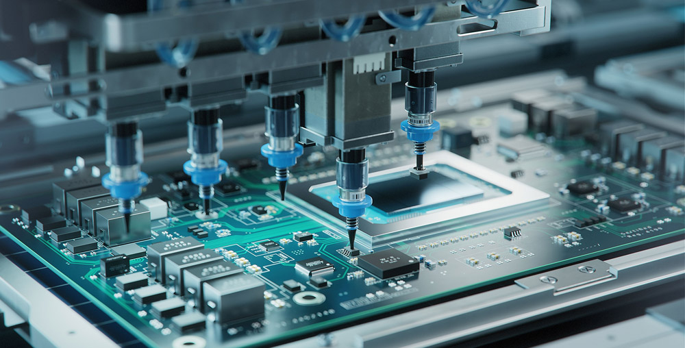
Liechtenstein’s electronic manufacturing sector, focused on industrial control and medical devices, depends on trusted PCB manufacturer in Liechtenstein for high-precision support. Its emphasis on precision drives demand for specialized services, yet balancing speed, cost and EU compliance poses a core challenge. A reliable PCB manufacturer in Liechtenstein must meet strict local standards and tight timelines, making it vital to identify trusted Liechtenstein PCB manufacturers, their capabilities, and pain points.
Top PCB Manufacturer in Liechtenstein
| Company Name | Core Business | Key Advantages | Process Capabilities | Lead Time |
| EBest Circuit Co., Limited | Single/double/multi-layer PCBs for industrial/medical | Localized service, strict QC, EU compliance | HDI, impedance control, ENIG/HASL | 7-10d (std), 3-5 day |
| Triesen Quick-Proto PCB GmbH | Prototypes/low-volume for R&D/startups | R&D-friendly pricing, fast iteration | 2-12 layer, laser drilling | 1-3d (proto), 4-7day |
| Liechtenstein Auto-Elec Circuits GmbH | Automotive-grade PCBs for control modules | IATF16949, high-temp resistance | Impedance matching, lead-free finish | 9-13d (std), 5-8 day |
| Balzers IoT PCB Technologie GmbH | IoT sensor PCBs for smart devices | Cost-effective, IoT-focused design | 4-8 layer, SMT integration | 5-9d (std), 2-4 day |
| Gamprin Precision PCB GmbH | Multi-layer PCBs for high-end industrial/medical | 16-layer capability, strict QA | HDI, blind/buried vias | 10-15d (std), 14-20 day |
Pain Points of PCB Manufacturer in Liechtenstein
- Prototyping delays often occur due to limited local production capacity, failing to meet rapid iteration needs of projects.
- High material costs and small order volumes lead to uncompetitive pricing for Liechtenstein PCB prototyping services.
- Design inconsistencies with manufacturing capabilities result in rework, as local suppliers lack proactive analysis support.
- Strict EU environmental regulations increase production costs, which are often passed on to customers by Liechtenstein PCB factory.
- Limited technical support for high-frequency and HDI PCBs, restricting the development of high-end electronic products.
- Unstable lead times for bulk orders due to reliance on imported raw materials and components.
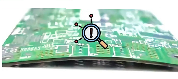
- Inadequate quality inspection for small-batch orders, leading to potential performance risks in final products.
Full-Process Guarantee from Requirement to Delivery
- Pre-production Design Optimization: Provide free DFM analysis to resolve design-manufacturing inconsistencies, reducing rework rates and saving project time for PCB Liechtenstein projects.
- Flexible Production Scheduling: Dedicated production lines for prototyping and small batches, eliminating delays caused by capacity constraints and ensuring rapid response.
- Cost Control System: Bulk material procurement and optimized production processes to offer competitive pricing without compromising quality for Liechtenstein PCB manufacturing.
- Compliance-Oriented Production: Integrate EU environmental standards into every process, ensuring products meet REACH and RoHS requirements without additional costs.
- High-End Technical Support: Professional team specialized in high-frequency and HDI PCBs, providing customized solutions for complex Liechtenstein PCB needs.
- Stable Supply Chain: Global strategic partnerships with raw material suppliers to avoid lead time fluctuations for bulk orders.
- Full-Process Quality Inspection: Implement AOI automatic detection and manual full inspection for all orders, regardless of batch size, to ensure zero defective products delivery.
- Real-Time Order Tracking: Digital management system allows customers to monitor production progress anytime, enhancing transparency for PCB manufacturer in Liechtenstein services.
Why Choose EBest(Best Technology) for PCB Manufacturer in Liechtenstein?
Reasons Why Choose EBest(Best Technology) for PCB Manufacturer in Liechtenstein:
- Competitive Pricing: Optimize cost structure via bulk material procurement, average reducing Liechtenstein PCB project budgets by 15%-20%, with transparent pricing no hidden costs.
- 24-Hour Rapid Prototyping: Dedicated emergency lines, finish prototyping in 24 hours for 6-layer and below standard specs, matching urgent iteration needs.
- High On-Time Delivery Rate: 99.2% on-time delivery for all orders, supported by global supplier partnerships and intelligent production scheduling.
- Strict Quality Control: 18-process full inspection (AOI/X-ray/electrical testing), product yield stable above 99.5%, zero defective delivery guaranteed.
- 19 Years of Industry Experience: Deep expertise in Liechtenstein PCB manufacturing, serving 500+ local clients, optimizing processes to cut 10% unnecessary costs.
- Free DFM Analysis: Proactive pre-production optimization, reducing design rework rate by 40%+, shortening project cycles by 72 hours on average.
- Comprehensive Certifications: Hold ISO9001:2015, ISO13485:2016, IATF16949, AS9100D, REACH & RoHS, covering 100% local high-end industry requirements.
- Localized Service: Nearby service center with ≤4-hour response, 200+ annual on-site support for Liechtenstein PCB company partners.
- Customized Solutions: Support 2-32 layer PCB customization, 60%+ order volume for small batches, adapting to diverse technical demands.
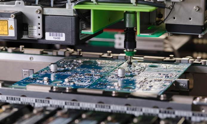
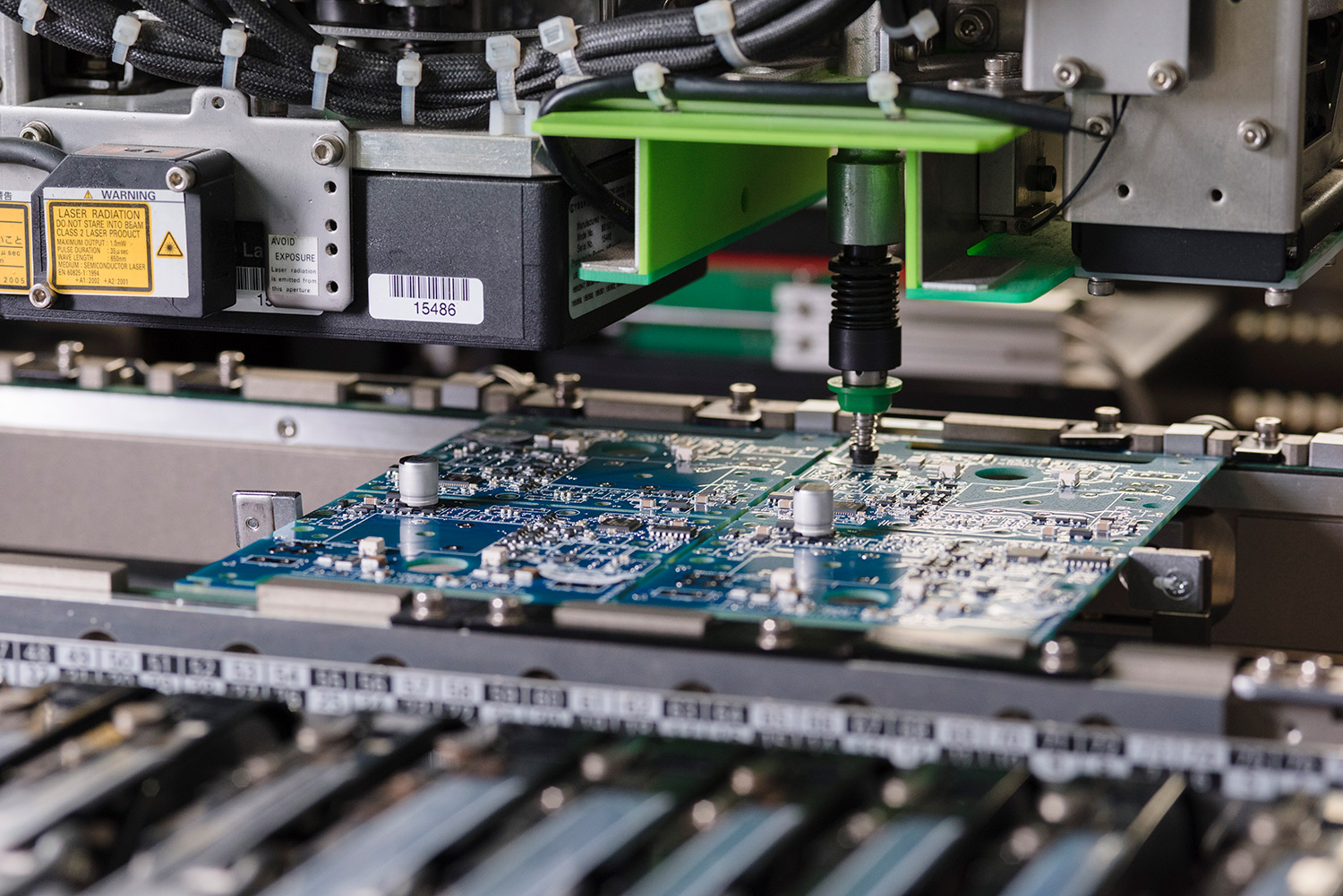
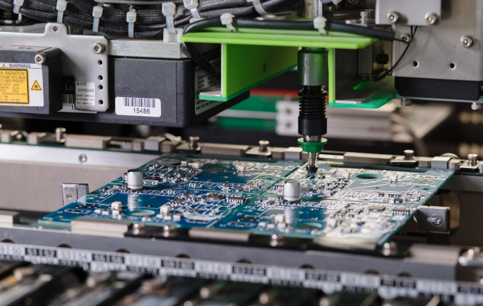
Liechtenstein PCB Prototyping Service We Can Offer
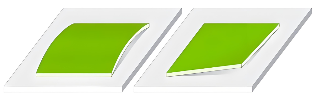
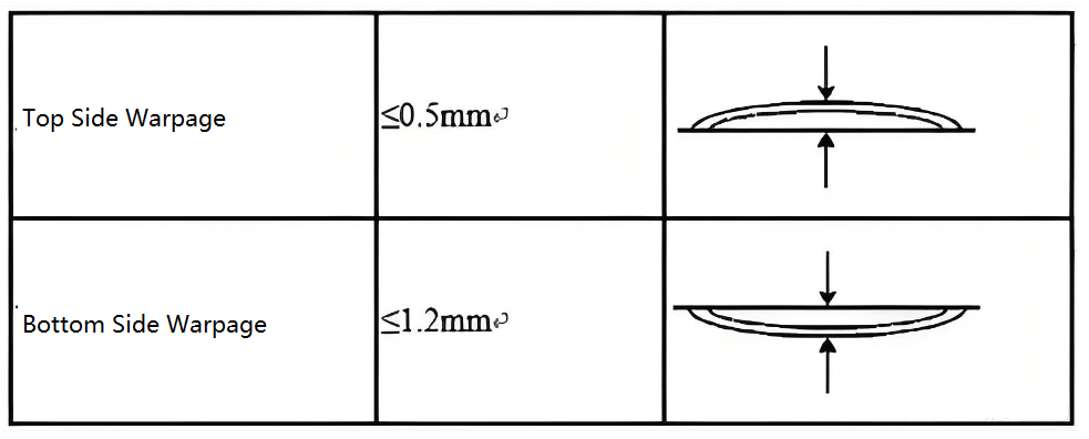
Our rapid prototyping service is tailored for Liechtenstein PCB projects, addressing the core pain points of local quick-turn needs with technical strength and efficient delivery. Equipped with 3 dedicated emergency production lines and mature precision manufacturing capabilities, we balance speed and accuracy to support rapid project iteration. We cover 2-24 layer prototyping, with minimum line width/spacing of 3mil/3mil and warpage controlled at ≤0.3%, ensuring compatibility with complex designs.
Unlike local services plagued by capacity constraints, our one-stop prototyping supports diverse processes (ENIG, HASL, OSP) and materials (FR-4, aluminum substrate), with impedance deviation controlled within ±10% for high-frequency demands. This combination of speed, precision and flexibility cuts local prototyping cycles by 40%+, making us the trusted partner for urgent, high-quality PCB Liechtenstein prototyping needs.

Lead Time of Our PCB Prototyping
| Layers | Normal Service | Fastest Service |
| 1 | 7 Days | 24 H |
| 2 | 8 Days | 24 H |
| 4 | 10 Days | 48 H |
| 6 | 10 Days | 72 H |
| 8 | 12 Days | 72 H |
| ≥10 | TBD | TBD |
Our PCB Manufacturing Capabilities
| Item | Capabilities |
| Layer Count | 1 – 32 Layers |
| Max Board Dimension | 2424″ (610610mm) |
| Min Board Thickness | 0.15mm |
| Max Board Thickness | 6.0mm – 8.0mm |
| Copper Thickness | Outer Layer: 1oz~30oz, Inner Layer: 0.5oz~30oz |
| Min Line Width/Line Space | Normal: 4/4mil (0.10mm); HDI: 3/3mil (0.076mm) |
| Min Hole Diameter | Normal: 8mil (0.20mm); HDI: 4mil (0.10mm) |
| Min Punch Hole Dia | 0.1″ (2.5mm) |
| Min Hole Spacing | 12mil (0.3mm) |
| Min PAD Ring(Single) | 3mil (0.075mm) |
| PTH Wall Thickness | Normal: 0.59mil (15um); HDI: 0.48mil (12um) |
| Min Solder PAD Dia | Normal: 14mil (0.35mm); HDI: 10mil (0.25mm) |
| Min Soldermask Bridge | Normal: 8mil (0.2mm); HDI: 6mil (0.15mm) |
| Min BAG PAD Margin | 5mil (0.125mm) |
| PTH/NPTH Dia Tolerance | PTH: ±3mil (0.075mm); NPTH: ±2mil (0.05mm) |
| Hole Position Deviation | ±2mil (0.05mm) |
| Outline Tolerance | CNC: ±6mil (0.15mm); Die Punch: ±4mil (0.1mm); Precision Die: ±2mil (0.05mm) |
| Impedance Controlled | Value>50ohm: ±10%; Value≤50ohm: ±5ohm |
| Max Aspect Ratio | 0.334027778 |
| Surface Treatment | ENIG, Flash Gold, Hard Gold Finger, Gold Plating(50mil), Gold finger, Selected Gold plating, ENEPIG, ENIPIG; HAL, HASL(LF), OSP, Silver Immersion, Tin Immersion |
| Soldermask Color | Green/White/Black/Yellow/Blue/Red |
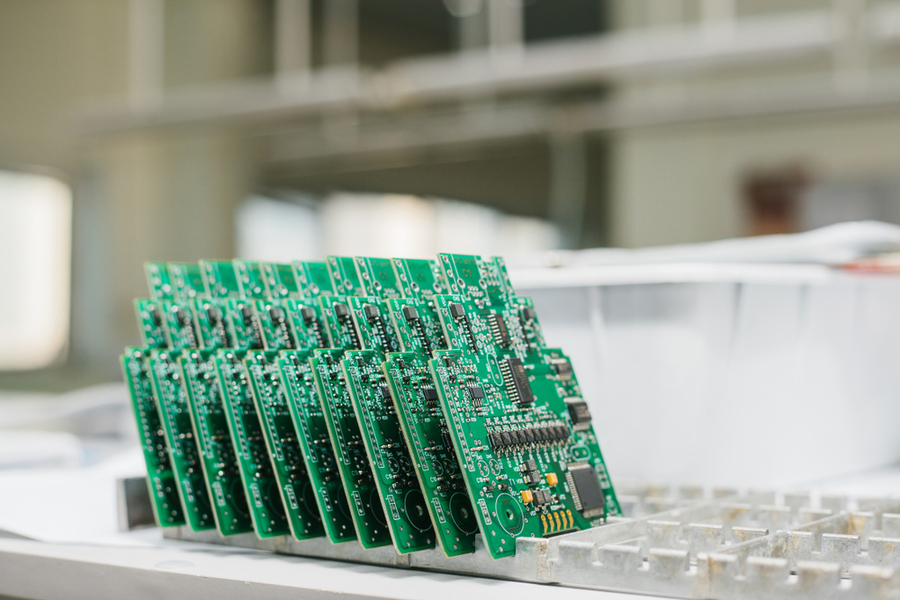
Our Quality Certifications for PCB Manufacturing
- ISO9001:2015: Full-process quality control for Liechtenstein PCB production, ensuring consistency and 99.5%+ stable yield.
- ISO13485:2016: Meets medical device requirements, enables full traceability, and guarantees compliance for medical Liechtenstein PCB.
- IATF16949: Automotive-specific certification with APQP/FMEA tools, satisfying high standards for in-vehicle PCB Liechtenstein.
- AS9100D: Aerospace-grade certification, recognized by Boeing/Airbus, qualifying for aviation Liechtenstein PCB supply.
- REACH & RoHS: EU environmental compliance for Liechtenstein PCB manufacturing, no extra cost, avoiding market access risks.
How to Get A Quote for PCB Prototyping Service?
Steps to Get A Quote for PCB Prototyping Service:
1. Submit Clear Requirements: Send standardized design files (Gerber, DXF) along with specific demands — material type (e.g., FR-4, aluminum substrate), layer count, surface finishing (ENIG/HASL/OSP), and order quantity. Files can be submitted via email or our official platform, with a recommended naming format for quick sorting.
2. Free Professional Evaluation: For standard Liechtenstein PCB prototyping requests, our team completes DFM analysis (to pre-check manufacturability and optimize designs) and cost assessment within 2 hours, reducing potential rework risks upfront.
3. Transparent Quotation Confirmation: Receive a detailed quotation with itemized costs, clear lead time commitment, and corresponding quality standards. No hidden fees — all expenses (processing, material, testing) are fully disclosed.
4. Simplified Order Placement: Confirm the quotation and pay the deposit (30% of total amount as standard). We immediately issue an order confirmation with detailed production milestones, including pre-production check and delivery cutoff times.
5. Real-Time Progress Tracking: Monitor Liechtenstein PCB manufacturing progress via our digital system anytime. Automatic notifications are sent for key nodes (production start, quality inspection, shipment), ensuring full process transparency.
Welcome to contact us if you have any request for PCB prototyping: sales@bestpcbs.com.