Do you struggle with ensuring consistent PCB cleanliness that meets industry requirements? PCB Cleanliness directly impacts product performance and longevity, especially in high-reliability sectors. This guide breaks down IPC-standard testing step-by-step, covering equipment, procedures, common issues, and solutions to help you achieve reliable results every time.
What is the IPC Standard for PCB Cleanliness?
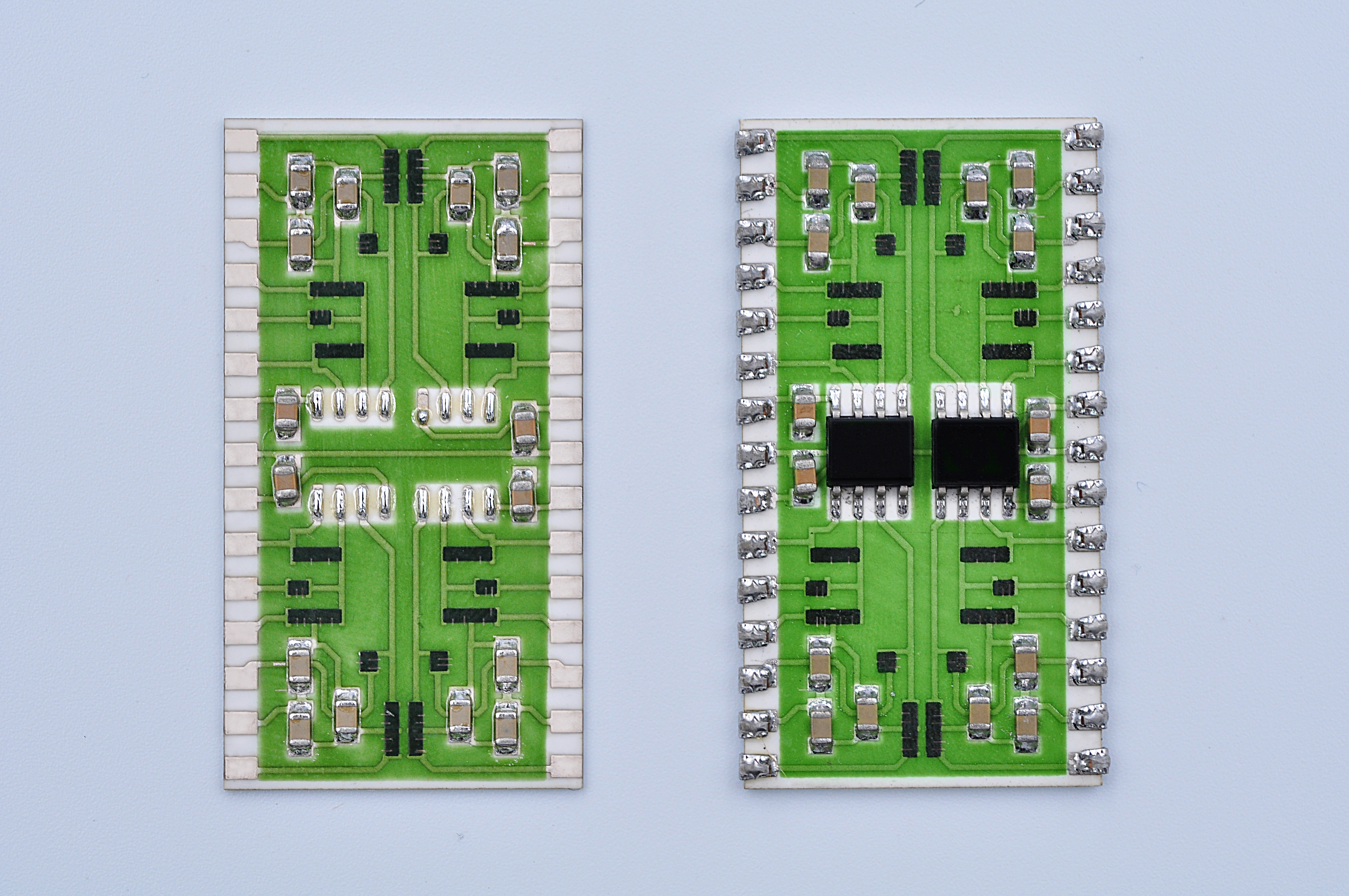
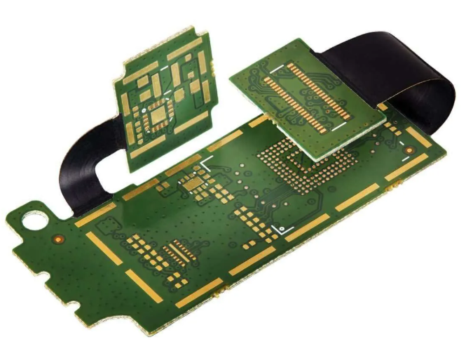
The IPC standard for PCB cleanliness is the industry benchmark for measuring residue and contaminants on PCB surfaces. The most relevant standards are IPC-6012 (for rigid PCBs) and IPC-610 (for PCB assemblies), which define acceptable contamination levels.
These standards specify limits for ionic and non-ionic residues, as well as particle contamination. For example, in aerospace applications, IPC standards require ionic residue levels below 1.5 μg/cm² to prevent corrosion and signal interference.
What Equipment and Tester are Required for PCB Cleanliness Testing?
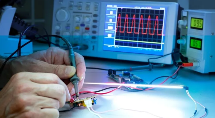
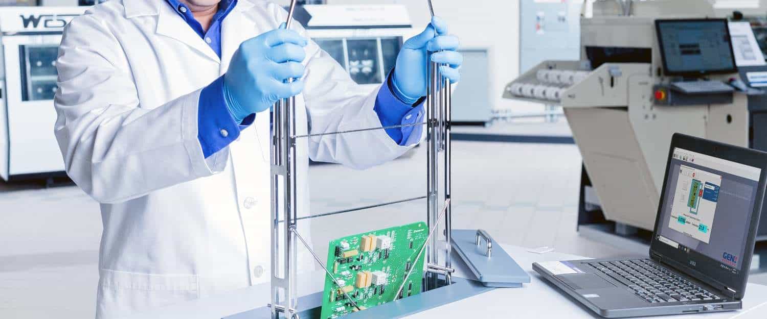
To ensure accurate, IPC-compliant PCB cleanliness testing, you need specialized PCB cleanliness testing equipment and PCB cleanliness tester that align with IPC-TM-650 procedures. Below is a detailed breakdown of essential equipment, their core functions, and key details to help you select reliable tools.
| Equipment Type | Core Function | Details for Reliability | IPC Compliance Note |
| PCB cleanliness tester | Measures overall residue levels, logs test data, and provides quick pass/fail results | Integrated software for data documentation; compatible with IPC-610/6012 standards | Ideal for preliminary screening before detailed ion chromatography testing |
| Ion Chromatograph | Critical for ion chromatography PCB cleanliness; detects and quantifies individual ionic residues (e.g., chloride, bromide) | Detects trace residues down to ppb levels; supports IPC-TM-650 2.3.28 method | Required for high-reliability sectors (aerospace, medical) to meet strict IPC limits |
| Extraction System | Removes residues from PCB surfaces using compatible solvents (e.g., isopropyl alcohol) | Closed-loop design to prevent solvent contamination; adjustable extraction time | Must follow IPC-TM-650 2.3.25 guidelines for solvent extraction procedures |
| Particle Counter | Evaluates PCB surface cleanliness by measuring particle size and count on PCB surfaces | Detects particles as small as 0.1μm; supports online/offline testing modes | Meets IPC requirements for particle contamination limits (e.g., 50μm max for industrial equipment) |
How to Perform PCB Cleanliness Testing with IPC Standard Correctly?
To perform PCB cleanliness testing correctly per IPC standards (IPC-TM-650 2.3.25/2.3.28, IPC-6012, IPC-610), follow these detailed, actionable steps, each aligned with industry best practices to ensure accuracy, repeatability, and compliance, with no unnecessary content.
Step 1: Select Test Specimen
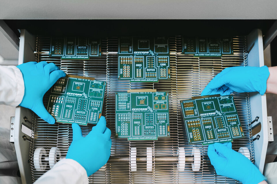
Choose representative PCBs or assemblies for testing. Handle with clean gloves to avoid introducing external contaminants. Ensure samples reflect actual production conditions.
Step 2: Prepare Solvent Mixture
Use a 75% isopropyl alcohol (IPA) and 25% deionized water solution as specified in IPC-TM-650 2.3.25. Ensure solvent purity to prevent false readings.
Step 3: Perform Ionic Extraction
Immerse the PCB in the solvent or apply via spray equipment. Extract ionic residues for 5–10 minutes using manual, dynamic, or static extraction methods. Avoid finger contact during handling.
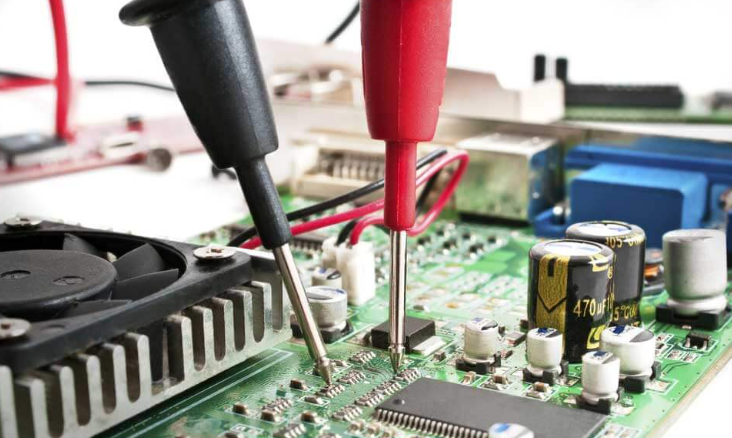
Step 4: Measure Resistivity/Conductivity
Transfer the solvent to a measurement cell or use an in-line system. Measure resistivity/conductivity changes. Convert readings to NaCl equivalent contamination (e.g., 1.56 μg/cm² limit per IPC-6012).
Step 5: Analyze via Ion Chromatography (IC)
For detailed ionic species breakdown (e.g., Cl⁻ ≤0.25 μg/cm², Br⁻ ≤0.25 μg/cm² per IPC-5704), use IC testing. This identifies specific ions beyond bulk contamination metrics.
Step 6: Conduct Surface Insulation Resistance (SIR) Testing
Evaluate electrochemical migration risk. Test at 85°C/85% RH with 45–50V DC bias for 7 days. Pass criteria require ≥10⁸ ohms from day 4 onward (IPC-TM-650 2.6.3.7).
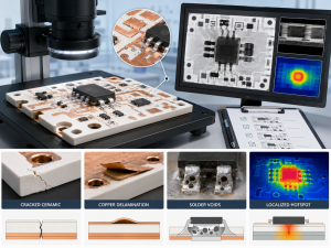
Step 7: Validate with Visual Inspection
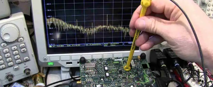
Inspect under 20–40X magnification (IPC-A-610) for residue, flux, or contaminants. High-density boards may require higher magnification for fine-pitch components.
Step 8: Interpret Results per Standards
Compare results against IPC benchmarks: IPC-5704 for bare boards, IPC-J-STD-001 for assembled boards. Class 2/3 products require objective evidence (e.g., SIR/IC data) for process qualification.
Step 9: Implement Corrective Actions
If limits are exceeded, adjust cleaning processes (e.g., ultrasonic cleaning parameters, solvent choice). Re-test to confirm improvements. Document all steps per IPC-5701/5702 guidelines.
Step 10: Maintain Process Control
Use ROSE testing as a process control tool (not pass/fail) per IPC-J-STD-001. Monitor trends to prevent reliability issues. Update testing methods as technology evolves (e.g., stricter limits for automotive/aerospace).
What is a PCB Ionic Cleanliness Test and How Does it Ensure Reliability?
A PCB ionic cleanliness test is a critical quality control measure that quantifies ionic residues on PCB surfaces. These residues typically come from manufacturing processes such as soldering flux, plating solutions, or handling contaminants and include substances like chlorides, bromides, and salts. The test uses methods like ROSE or ion chromatography to extract and measure these residues, ensuring compliance with IPC standards.
Ionic residues pose significant risks to PCB performance as they attract moisture, leading to corrosion of metal components and conductive paths. Over time, this corrosion can cause short circuits, signal degradation, and complete PCB failure. The test directly mitigates these risks by ensuring residues stay within IPC limits tailored to application needs.
In high-reliability sectors, the PCB ionic cleanliness test is essential for long-term reliability. For medical device PCBs, ionic residues can leach into bodily fluids and compromise device safety. For aerospace PCBs, even trace residues can cause corrosion in extreme environments, threatening in-flight functionality. The test ensures these critical components meet strict IPC guidelines, preventing costly failures and ensuring product durability.
How Does Ion Chromatography Apply to PCB Cleanliness Measurement?
Ion chromatography PCB cleanliness is a precise, IPC-compliant method for measuring ionic residues on PCB surfaces, critical for high-reliability applications. It complements basic PCB cleanliness tester screenings by identifying and quantifying individual ionic contaminants, rather than just providing a total residue value.
The application process aligns with IPC-TM-650 2.3.28 guidelines. First, residues are extracted from the PCB using a compatible solvent, then the extract is injected into the ion chromatograph. The device separates ions based on their charge and affinity for the stationary phase, allowing for precise detection of specific residues like chlorides, bromides, and flux salts.
Its precision makes it ideal for strict IPC Class 3 applications. For aerospace PCBs, it detects trace residues as low as 0.1 μg/cm², a level critical for preventing corrosion in extreme flight environments. For medical device PCBs, it ensures no harmful ionic residues leach into bodily fluids, meeting both IPC and medical regulatory standards.
Unlike simpler methods like the ROSE test, ion chromatography provides detailed residue breakdowns. This helps identify the source of contamination, such as inadequate flux cleaning or plating solution residues, enabling targeted corrective actions to maintain PCB Cleanliness compliance.
How to Evaluate PCB Surface Cleanliness According to IPC Guidelines?
Here are methods to evaluate PCB surface cleanliness according to IPC guidelines:
- Sample Selection: Choose PCBs or assemblies that represent typical production batches. Handle samples with clean gloves to prevent contamination. Ensure samples mirror actual product conditions per IPC-TM-650 2.1.1.
- Solvent Preparation: Prepare a 75% isopropyl alcohol (IPA) and 25% deionized water solution, as defined in IPC-TM-650 2.3.25. Verify solvent purity to avoid skewed results.
- Ionic Residue Extraction: Submerge or spray the PCB with the solvent for 5–10 minutes. Use manual, dynamic, or static extraction methods to dislodge ionic contaminants. Avoid direct contact during handling.
- Conductivity Measurement: Transfer the solvent to a conductivity meter cell. Measure conductivity changes and convert to NaCl equivalent contamination (e.g., ≤1.56 μg/cm² per IPC-6012).
- Ion Chromatography (IC) Analysis: Perform IC testing to identify specific ionic species (e.g., Cl⁻ ≤0.25 μg/cm², Br⁻ ≤0.25 μg/cm² per IPC-5704). This quantifies individual ion levels beyond bulk contamination.
- Surface Insulation Resistance (SIR) Test: Evaluate electrochemical migration risk by exposing the PCB to 85°C/85% RH with 45–50V DC bias for 7 days. Pass criteria require ≥10⁸ ohms from day 4 onward (IPC-TM-650 2.6.3.7).
- Visual Inspection: Inspect the PCB under 20–40X magnification (IPC-A-610) to detect residues, flux remnants, or contaminants. High-density boards may require higher magnification for fine-pitch components.
- Result Interpretation: Compare results against IPC benchmarks: IPC-5704 for bare boards, IPC-J-STD-001 for assembled boards. Class 2/3 products need objective evidence (e.g., SIR/IC data) for process qualification.
- Corrective Action Implementation: If contamination exceeds limits, adjust cleaning processes (e.g., ultrasonic parameters, solvent type). Re-test to validate improvements. Document changes per IPC-5701/5702.
- Process Control Monitoring: Use ROSE testing as a trend-monitoring tool (not pass/fail) per IPC-J-STD-001. Track data to prevent reliability issues. Update methods for evolving standards (e.g., stricter limits for automotive/aerospace).
How to Maintain PCB Cleanliness Testing Equipment for Accurate Results?
Maintaining PCB cleanliness testing equipment ensures accurate results and prolongs equipment life through systematic care and best practices.
- Regular Calibration: Schedule periodic calibration of testing devices (e.g., Surface Insulation Resistance testers) to maintain measurement accuracy and detect drift.
- Filter and Component Checks: Clean or replace filters monthly, inspect seals/joints for leaks, and monitor oil levels in transformers to prevent contamination-induced failures.
- Proper Loading: Use baskets/trays to secure PCBs during testing, avoiding overloading to ensure uniform exposure to cleaning solutions and prevent missed contamination spots.
- Cleaning Agent Selection: Match solvents to flux types (e.g., aqueous solutions for water-soluble fluxes, ultrasonic systems for rosin-based residues) to optimize residue removal without damaging components.
- Environmental Controls: Maintain ventilation, avoid temperatures above 300°C near equipment, and use spill trays to prevent PCB contact with combustion sources or environmental contaminants.
- Operator Training: Train staff in safe handling, maintenance protocols, and troubleshooting to minimize human error and ensure consistent testing procedures.
- Consumables Management: Replace worn brushes, nozzles, and filters regularly to maintain cleaning efficiency and prevent recontamination.
- Maintenance Logs: Document all maintenance activities, including dates, tasks performed, and issues resolved, to track equipment performance and plan proactive repairs.
How to Interpret Results from a PCB Ionic Cleanliness Test Properly?
Proper interpretation of PCB ionic cleanliness test results ensures reliability and prevents failures by identifying contamination sources and guiding corrective actions.
- Compare Results to Standards: Align test data with IPC-TM-650 or other industry limits to determine if ionic contamination exceeds acceptable levels, indicating potential reliability risks.
- Identify Contaminant Types: Use techniques like ion chromatography to pinpoint specific ions (e.g., chloride, sulfate) and trace their origins to manufacturing, cleaning, or handling processes.
- Analyze Spatial Distribution: Map contamination hotspots on the PCB to correlate with assembly steps (e.g., soldering, flux application) and identify process gaps.
- Evaluate Environmental Impact: Consider humidity, temperature, and storage conditions that may exacerbate ionic activity or introduce new contaminants.
- Validate Cleaning Efficacy: Assess whether cleaning processes (e.g., aqueous wash, solvent cleaning) effectively removed residues by comparing pre- and post-cleaning test results.
- Monitor Trends Over Time: Track test results across batches to detect process drift, seasonal variations, or supplier-related material changes.
- Integrate with Other Tests: Combine ionic cleanliness data with surface insulation resistance (SIR) or electrochemical migration tests for a comprehensive reliability assessment.
- Implement Corrective Actions: Based on findings, adjust cleaning parameters, update material specifications, or refine handling procedures to mitigate contamination risks.
What Are the Common PCB Cleanliness Failures and How to Avoid Them?
Q1: Why do PCBs fail PCB cleanliness testing even after cleaning?
A1: The most common cause is incomplete flux removal. Flux residues can hide in tight spaces (e.g., between components). Solution: Use a spray-in cleaning system to reach hard-to-access areas, then re-test with ion chromatography.
Q2: How does PCB surface cleanliness affect industrial equipment performance?
A2: Poor PCB surface cleanliness leads to dust buildup and residue accumulation, which can cause overheating and short circuits. Solution is to implement a strict cleanroom protocol during assembly and conduct regular PCB surface cleanliness checks.
Q3: Can ion chromatography PCB cleanliness testing detect all ionic residues?
A3: Ion chromatography can detect most common ionic residues (e.g., flux salts, contaminants from manufacturing). Solution is to use a combination of ion chromatography and a PCB cleanliness tester for comprehensive coverage.
Q4: What causes inconsistent results from PCB cleanliness testing equipment?
A4: Inconsistencies often come from uncalibrated equipment or contaminated solvents. Solution is to calibrate equipment monthly and replace solvents every 2-3 months to ensure accuracy.
Q5: How to ensure PCB cleanliness compliance for medical device PCBs?
A5: Medical device PCBs require strict adherence to IPC-610 and additional regulatory standards. Solution is to conduct both PCB ionic cleanliness test and non-ionic residue testing, and document all results for compliance audits.