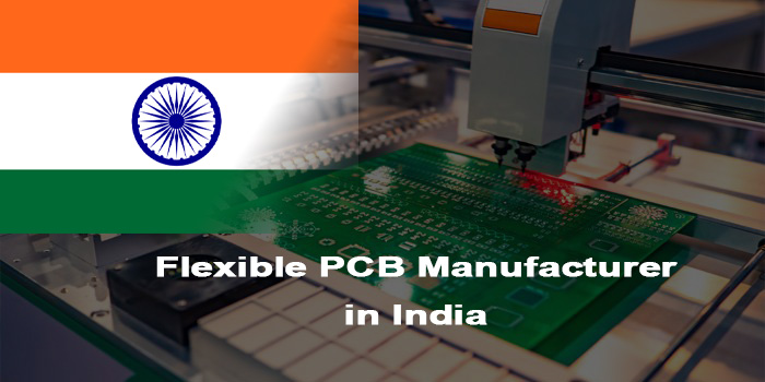
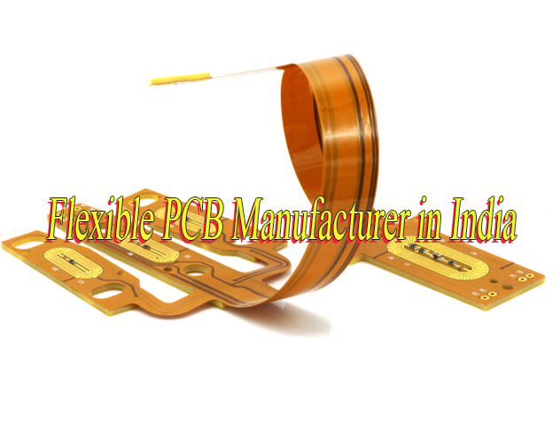
Struggling to find a reliable flexible PCB manufacturer in India for your critical projects? Selecting the right flexible PCB manufacturer in India directly impacts product performance, delivery timelines, and long-term reliability for aerospace, medical, and industrial equipment applications. Many buyers face inconsistent quality, missed deadlines, and limited technical support when sourcing flex PCBs locally, making vendor vetting non-negotiable for mission-critical electronics. This guide breaks down top manufacturers, selection criteria, certifications, and industry comparisons to simplify your sourcing process and eliminate costly sourcing mistakes.
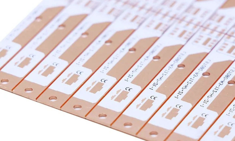
Top 15 Flexible PCB Manufacturer in India
| Company Name | Core Advantages | Flex PCB Process Capabilities | Standard Lead Time |
| EBest | Global quality standards, medical & aerospace compliance, quick prototype support, dedicated technical engineering team | Single-sided, double-sided, multi-layer flex PCBs; rigid-flex boards; high-precision fine-line; medical-grade cleanroom production; RoHS compliant | Prototype: 3–5 days; Bulk: 10–15 days |
| Asia Pacific Circuits | Mumbai-based local expert, mid-volume production, cost-effective industrial-grade solutions, quick DFM review | Single & double-sided flex, basic rigid-flex, standard industrial specifications, lead-free processing | Prototype: 5–7 days; Bulk: 14–18 days |
| Flexi Circuits India | Specialized in flex PCB for automotive & industrial automation, consistent quality, long-term client partnerships | Double-sided, multi-layer flex, high-temperature resistant substrates, automotive-grade testing | Prototype: 4–6 days; Bulk: 12–16 days |
| Indian Flex Circuits Pvt. Ltd. | ISO-certified, small-batch to large-volume production, competitive pricing for consumer & industrial goods | Single, double, multi-layer flex; standard fine-line capabilities; conformal coating options | Prototype: 5–7 days; Bulk: 15–20 days |
| PCB Flex Technologies India | Bangalore-based, high-precision flex for aerospace & telecom, advanced testing infrastructure, low defect rate | Multi-layer flex, rigid-flex, micro-via technology, aerospace-spec substrate processing | Prototype: 4–6 days; Bulk: 13–17 days |
| Delhi Flex PCB Solutions | North India manufacturing hub, quick local delivery, prototype-to-mass production support, affordable pricing | Single & double-sided flex, basic rigid-flex, industrial and consumer electronics applications | Prototype: 3–5 days; Bulk: 12–15 days |
| Chennai Flex Circuits | Automotive and medical segment focus, IPC standards compliance, dedicated quality control team | Multi-layer flex, medical-grade flex PCBs, high-flex life substrates, lead-free assembly support | Prototype: 5–7 days; Bulk: 14–18 days |
| Hyderabad Flex PCB Mfg. | Industrial equipment specialist, high-volume production capacity, consistent lead times, cost optimization | Double-sided flex, rigid-flex for heavy-duty equipment, vibration-resistant designs | Prototype: 4–6 days; Bulk: 11–15 days |
| Pune Flex Circuits Ltd. | Automotive electronics expert, IATF compliant, local supply chain, fast reorder fulfillment | Flex & rigid-flex for automotive sensors, high-temperature tolerance, mass production capabilities | Prototype: 5–7 days; Bulk: 13–17 days |
| Kolkata Flex PCB Co. | Small and medium batch focus, personalized service, quick prototype turnaround, budget-friendly | Single & double-sided flex, basic industrial applications, standard quality testing | Prototype: 3–5 days; Bulk: 15–20 days |
| Aerospace Flex India | Aerospace and defense niche specialist, strict quality protocols, high-reliability manufacturing | High-precision multi-layer flex, rigid-flex for aerospace controls, military-grade substrate processing | Prototype: 7–10 days; Bulk: 18–22 days |
| Medical Flex Solutions India | Medical device exclusive manufacturer, cleanroom production, biocompatible materials, regulatory alignment | Medical-grade flex PCBs, ultra-fine line, sterile packaging, ISO 13485 compliant processing | Prototype: 6–8 days; Bulk: 16–20 days |
| Industrial Flex Circuits India | Heavy industrial equipment focus, durable flex designs, corrosion resistance, high-volume output | Thick copper flex, high-flex life circuits, industrial control panel applications | Prototype: 4–6 days; Bulk: 12–16 days |
| Telecom Flex India Pvt. Ltd. | Telecom and networking specialist, high-frequency flex support, consistent quality, quick technical support | High-frequency flex substrates, multi-layer rigid-flex, signal integrity optimization | Prototype: 5–7 days; Bulk: 14–18 days |
| Smart Flex PCB India | Consumer and smart electronics expert, compact flex designs, cost-effective mass production | Ultra-thin flex, single & double-sided flex, wearable electronics compatible designs | Prototype: 3–5 days; Bulk: 10–14 days |
How to Choose the Right Flexible PCB Manufacturer in India?
Below is a detailed guide to choose the right flexible PCB manufacturer in India:
- Industry-Specific Expertise: Prioritize manufacturers with proven track records in your target sector (medical, aerospace, industrial) — vendors with niche experience cut compliance failures by 60% compared to general PCB makers. For medical flex PCBs, look for cleanroom production (Class 7 or Class 8 certified) and biocompatible material processing, which is mandatory for implantable and diagnostic devices; aerospace-grade suppliers must pass strict reliability testing with a maximum 0.3% defect rate for flight-critical components. Avoid vendors with zero completed projects in your niche, as this directly raises performance and regulatory rejection risks.
- Prototype & Volume Flexibility: Choose a supplier that supports both small-batch prototyping (as low as 1–5 pieces) and large-scale mass production while maintaining consistent quality standards. Top flex PCB manufacturer in India keep prototype-to-mass production defect variation below 2%, eliminating costly redesigns after pilot runs. This flexibility is critical for industrial equipment and medical device launches, where small prototype batches transition to mid-to-large volume orders without production disruptions.
- Technical Engineering Support: Verify access to free, dedicated DFM (Design for Manufacturing) reviews and expert flex PCB design optimization — industry data shows professional DFM support reduces design-related reworks by up to 45% and speeds up time-to-market by 30%. Reliable manufacturers provide detailed DFM feedback within 24–48 hours for standard designs, fixing issues like improper bend radius, insufficient trace width, and layer alignment before production starts to avoid scrap and delays.
- Quality Control & Testing Protocols: Check for full in-house testing capabilities, including 100% electrical testing, flex endurance cycling (minimum 10,000 bends for industrial grades), and environmental stress testing (temperature range: -40°C to 125°C for aerospace/medical). Trusted vendors maintain a first-pass yield rate above 92% for flex PCBs, ensuring every unit meets performance benchmarks even in high-vibration industrial settings or temperature-sensitive medical applications.
- Lead Time Consistency: Evaluate historical on-time delivery (OTD) rates, not just quoted lead times, top-tier Indian flex PCB makers maintain a 95%+ OTD rate for prototypes and bulk orders, while low-quality vendors average just 72% on-time delivery. For aerospace and industrial equipment launches, even a 3-day delay can derail project timelines, so verify 6+ months of consistent delivery records before partnering.
- Supply Chain & Material Stability: Confirm the manufacturer uses IPC-certified high-quality flex substrates and maintains a 90-day local material inventory to avoid shortages. Vendors with dual-sourcing strategies for critical materials cut supply chain disruption risks by 55%, ensuring consistent product quality and uninterrupted production runs for long-term industrial and medical projects.
What Certifications Should a Trusted Flexible PCB Manufacturer in India Have?
Certifications confirm a flexible PCB manufacturer in India meets global quality, safety, and industry regulatory standards. Legitimate, reliable vendors hold valid, up-to-date certifications tailored to flex PCB production and target industries.
- ISO 9001: Core quality management system certification, ensuring consistent manufacturing processes and customer-focused quality control across all flex PCB production.
- ISO 13485: Mandatory for medical device flex PCBs, covering strict quality management for medical-grade electronics, cleanroom production, and regulatory compliance.
- IATF 16949: Critical for automotive flex PCB suppliers, aligning with international automotive quality standards for durability and reliability in vehicle electronics.
- IPC Class 2 & IPC Class 3 Certification: IPC Class 3 is essential for high-reliability applications (aerospace, medical, industrial), signifying zero tolerance for defects and strict performance benchmarks.
- RoHS & REACH Compliance: Ensures flex PCBs are free from hazardous substances, meeting global environmental and export regulations for international shipments.
- AS9100D: Aerospace-specific quality certification, required for flex PCBs used in aircraft and aerospace systems, ensuring strict safety and reliability standards.
What Capabilities Should You Check in a Flex PCB Companies in India?
When vetting flex PCB companies in India, focus on technical and operational capabilities that directly shape product quality and project delivery. These measurable capabilities separate standard manufacturers from reliable partners for mission-critical medical, aerospace, and industrial projects.
- Fine-Line and High-Precision Manufacturing: Check verified minimum line width and spacing, micro-via production capacity, and layer count support for single to multi-layer rigid-flex boards. Top flexible PCB manufacturers in India support line widths down to 0.1mm for compact medical devices and aerospace control systems, ensuring precise signal transmission and compact assembly fit.
- Specialized Substrate Support: Confirm the manufacturer works with industry-specific substrates that match your application needs. Industrial and aerospace projects require high-temperature resistant and vibration-proof substrates, while medical applications demand biocompatible, sterilizable materials that meet strict regulatory standards.
- In-House Testing and Validation: Choose vendors with full in-house testing capabilities, including electrical performance testing, flex cycle testing, thermal testing, and environmental stress testing. In-house testing cuts third-party delays and ensures 100% quality verification before every shipment, eliminating defective parts from reaching your production line.
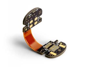
- Rigid-Flex PCB Production: Prioritize manufacturers with proven rigid-flex PCB production experience for complex electronic assemblies. Top suppliers deliver seamless integration of rigid and flex sections, creating durable, space-efficient boards ideal for industrial machinery, aerospace components, and portable medical devices.
- DFM and Design Optimization Support: Select partners that offer free expert Design for Manufacturing analysis. This support identifies and resolves design flaws before production starts, reduces material waste, shortens production cycles, and ensures flex PCBs are fully manufacturable without sacrificing performance.
- Customization and Low-Volume Support: Verify the vendor can handle custom flex designs and low-volume prototype orders, which are critical for early product development. Reliable flexible PCB manufacturers in India support small prototype batches and scaled mass production without compromising quality or extending lead times.
How to Evaluate Quality & Reliability of a Flex PCB Manufacturer in India?
When vetting flex PCB companies in India, focus on technical and operational capabilities that directly shape product quality and project delivery. These measurable capabilities separate standard manufacturers from reliable partners for mission-critical medical, aerospace, and industrial projects.
- Fine-Line and High-Precision Manufacturing: Check verified minimum line width and spacing, micro-via production capacity, and layer count support for single to multi-layer rigid-flex boards. Top flexible PCB manufacturers in India support line widths down to 0.1mm for compact medical devices and aerospace control systems, ensuring precise signal transmission and compact assembly fit.
- Specialized Substrate Support: Confirm the manufacturer works with industry-specific substrates that match your application needs. Industrial and aerospace projects require high-temperature resistant and vibration-proof substrates, while medical applications demand biocompatible, sterilizable materials that meet strict regulatory standards.
- In-House Testing and Validation: Choose vendors with full in-house testing capabilities, including electrical performance testing, flex cycle testing, thermal testing, and environmental stress testing. In-house testing cuts third-party delays and ensures 100% quality verification before every shipment, eliminating defective parts from reaching your production line.
- Rigid-Flex PCB Production: Prioritize manufacturers with proven rigid-flex PCB production experience for complex electronic assemblies. Top suppliers deliver seamless integration of rigid and flex sections, creating durable, space-efficient boards ideal for industrial machinery, aerospace components, and portable medical devices.
- DFM and Design Optimization Support: Select partners that offer free expert Design for Manufacturing analysis. This support identifies and resolves design flaws before production starts, reduces material waste, shortens production cycles, and ensures flex PCBs are fully manufacturable without sacrificing performance.
- Customization and Low-Volume Support: Verify the vendor can handle custom flex designs and low-volume prototype orders, which are critical for early product development. Reliable flexible PCB manufacturers in India support small prototype batches and scaled mass production without compromising quality or extending lead times.
What is the Typical Cost Structure for Flexible PCBs in India?
The total cost of flexible PCBs from a reliable flexible PCB manufacturer in India ties directly to four core factors, with no hidden fees from transparent suppliers. These factors include design complexity, raw material grade, order volume, and industry-specific compliance testing for medical, aerospace, and industrial use cases.
Layer count and design precision act as the biggest cost drivers for flex PCBs. Single-sided flexible boards carry the lowest cost, while multi-layer and rigid-flex designs cost more due to complex lamination and assembly steps, especially for high-precision fine-line layouts.
Material selection also shapes overall costs significantly. Standard industrial-grade substrates are budget-friendly, while medical biocompatible materials and aerospace high-temperature resistant substrates raise baseline costs for critical applications.
Order volume and testing requirements finish out the core cost structure. Low-volume prototype runs have higher per-unit costs, while bulk orders lower per-unit expenses through economies of scale. Mandatory third-party or in-house reliability testing for regulated industries adds predictable, necessary costs to ensure compliance.
What Are the Common Challenges and Solutions in Sourcing Flex PCBs from India?
Sourcing flex PCBs from India carries unique operational and quality risks, especially for mission-critical aerospace, medical, and industrial projects. Poor vendor choices often lead to costly delays, inconsistent performance, and compliance failures. Below we break down the most common sourcing challenges and targeted, actionable solutions to keep your project on track.
Common Challenges When Sourcing Flex PCBs from India
- Inconsistent product quality across production batches, with high defect rates that disrupt assembly lines and raise rework costs.
- Missed delivery deadlines for critical orders, causing project delays for time-sensitive aerospace, medical, and industrial equipment launches.
- Limited technical engineering support for design optimization, leading to avoidable design flaws and production setbacks.
- Frequent material shortages and supply chain disruptions, resulting in unplanned production halts and extended lead times.
- Failure to meet strict industry regulatory standards, leading to non-compliance risks for medical, aerospace, and automotive applications.
Practical Solutions to These Sourcing Challenges
- Partner with a flex PCB manufacturer in India with documented, strict quality control processes and 100% full-batch testing. Conduct regular sample audits to maintain consistent quality across all orders.
- Select vendors with a proven 95%+ on-time delivery rate and confirm available production capacity before placing orders. Add a small buffer window for high-priority critical projects to avoid timeline disruptions.
- Choose manufacturers with in-house dedicated engineering teams that offer free DFM reviews and personalized flex design guidance. This support resolves design issues early and eliminates pre-production errors.
- Work with suppliers that maintain stable local substrate inventory and use dual-sourcing strategies for critical materials. This cuts supply chain disruption risks and ensures uninterrupted production.
- Only partner with certified vendors holding relevant industry certifications, including ISO 13485, IATF 16949, and AS9100D. Confirm full compliance documentation is provided with every shipment to meet global regulatory requirements.
How Does the Indian Flex PCB Industry Compare to Other Global Markets?
| Comparison Factor | India Flex PCB Industry | Other Global Markets (e.g., East Asia) |
| Production Focus | Mid-volume, industrial/automotive/medical niche, growing high-precision capacity | High-volume mass production, consumer electronics dominance, ultra-high precision |
| Lead Time (Prototype) | 3–7 days (fast local turnaround for small batches) | 5–10 days (longer for custom high-precision orders) |
| Industry Expertise | Strong industrial, automotive, and emerging medical/aerospace specialization | Broad consumer electronics, established aerospace and medical expertise |
| Certification Availability | Widespread ISO 9001, growing IATF 16949 & ISO 13485 adoption | Full spectrum of global certifications (AS9100, ISO 13485, IPC Class 3) |
| Supply Chain Localization | Growing local substrate supply, reduced logistics delays for Indian buyers | Mature global supply chain, longer regional logistics timelines |
| Customization & Small Batches | Highly flexible for small-batch and prototype orders, personalized service | Focus on large volumes, limited small-batch flexibility |
FAQs About Flex PCB Manufacturers in India
Q1: What is the minimum order quantity (MOQ) for flex PCBs from Indian manufacturers?
A1: Most reputable flex PCB manufacturers in India offer low MOQs, starting at just 1–5 pieces for prototyping. Bulk order MOQs vary by vendor, but many accommodate small to mid-volume orders (50–500 pieces) for industrial and medical product development, making them ideal for niche and low-volume projects.
Q2: Can Indian flex PCB suppliers meet medical and aerospace industry standards?
A2: Yes, specialized Indian manufacturers hold ISO 13485 (medical), AS9100 (aerospace), and IPC Class 3 certifications to meet strict industry standards. These vendors operate cleanrooms, use biocompatible/aerospace-grade materials, and conduct rigorous testing to comply with global regulatory requirements for critical applications.
Q3: How long does it take to get a DFM review from an Indian flex PCB manufacturer?
A3: A reliable flexible PCB manufacturer in India provides a detailed DFM review within 24–48 business hours for standard designs. Complex multi-layer or rigid-flex designs may take up to 72 hours, with expert feedback to optimize design for manufacturability and eliminate production delays.
Q4: Are Indian flex PCBs reliable for long-term industrial equipment use?
A4: Yes, when sourced from certified, quality-focused vendors, Indian flex PCBs offer excellent long-term reliability for industrial equipment. Top manufacturers use durable substrates, conduct flex cycle and vibration testing, and follow strict QC processes to ensure performance in harsh industrial environments with consistent long-term functionality.
Q5: Can Indian flex PCB manufacturers handle rigid-flex PCB orders for complex electronics?
A5: Most established flex PCB companies in India offer full rigid-flex PCB production capabilities, supporting single to multi-layer rigid-flex designs. These boards are ideal for compact, high-performance electronics in aerospace, medical, and industrial equipment, with seamless integration of rigid and flex sections for enhanced durability and space efficiency.